3725f.pm6
LTC3725
1
3725f
FEATURES
DESCRIPTIO
U
APPLICATIO S
U
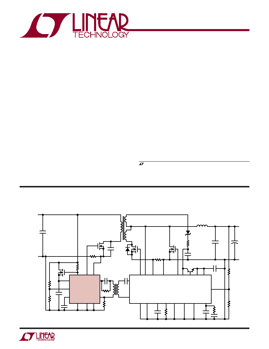
TYPICAL APPLICATIO
U
Isolated 48V Telecommunication Systems
Internet Servers and Routers
Distributed Power Step-Down Converters
Automotive and Heavy Equipment
High Speed Gate Driver for Forward Converter
On-Chip Rectifier and Self-Starting Architecture
Eliminates Need for Separate Gate Drive Bias
Supply
Wide Input Voltage Supply Range: 9V and Up
Linear Regulator Controller for Fast Start-Up
Precision UVLO with Adjustable Hysteresis
Overcurrent Protection
Volt-Second Limit Prevents Transformer Core
Saturation
Voltage Feedforward for Fast Transient Response
Available in 10-Lead MSOP Package
Single-Switch Forward
Controller and Gate Driver
The LTC
®
3725 is a controller for a single-switch forward
converter and includes an on-chip gate driver.
For secondary-side control, combine the LTC3725 with
the LTC3706 PolyPhase
®
secondary-side synchronous
forward controller to create a complete forward converter
using a minimum of discrete parts. A proprietary scheme
is used to multiplex gate drive signals across the isolation
barrier through a tiny pulse transformer. The on-chip
rectifier and the same pulse transformer provide gate drive
bias power.
Alternatively, the LTC3725 can be used as a standalone
voltage mode controller in a primary-side control architec-
ture with optoisolator feedback. Voltage feedforward pro-
vides excellent line regulation and transient response.
36V-72V to 3.3V/30A Isolated Single-Switch Forward Converter
, LTC and LT are registered trademarks of Linear Technology Corporation. PolyPhase is
a registered trademark of Linear Technology Corporation. All other trademarks are the
property of their respective owners. Patent Pending
FB/IN
+
1
µF
100V
×2
V
IN
+
36V TO 72V
V
IN
2.2nF
200V
10
µF
100
µF
6.3V
×2
220
µF
6.3V
V
OUT
+
3.3V
30A
V
OUT
47nF
470pF
33nF
B0540W
Si7450DP
33nF
15k
1
µF
0.1
µF
0.030
1W
1
µF
2.2
µF
0.0012
1W
HAT2165
×2
HAT2165
×2
L1
0.85
µH
T2
·
·
162k
L1: PULSE PA1294.910
T1: PULSE PA0815
T2: PULSE PA0297
5.1k
3.3k
100k
2.74k
604
3725 TA01
1.2
1/4W
100k
FS/IN
V
CC
UVLO
SSFLT
I
S
GATE
LTC3725
NDRV
GND
PGND
V
SLMT
365k
FDC2512
T1
·
·
PT
+
FG SW
I
S
I
S
+
SG V
IN
V
CC
MODE
NDRV
GND PGND RUN/SS SLP REGSD FS/SYNC
I
TH
PHASE
FCX491A
PT
FB
LTC3706
+
·
LTC3725
2
3725f
Power Supply (V
CC
) ................................... 0.3V to 15V
External NMOS Drive (NDRV) .................... 0.3V to 20V
NDRV to V
CC ...........................................................
0.3V to 5V
Soft-Start Fault, Feedback,
Frequency Set, Transformer
Inputs (SSFLT, FB/IN
+
, FS/IN
) .................. 0.3V to 15V
All Other Pins (V
SLMT
, I
S
, UVLO) ................. 0.3V to 5V
Peak Output Current <1
µs (GATE) ............................. 2A
Operating Ambient Temperature Range .. 40
°C to 85°C
Operating Junction Temperature (Note 2) ............ 125
°C
Storage Temperature Range ................. 65
°C to 150°C
Lead Temperature (Soldering, 10 sec).................. 300
°C
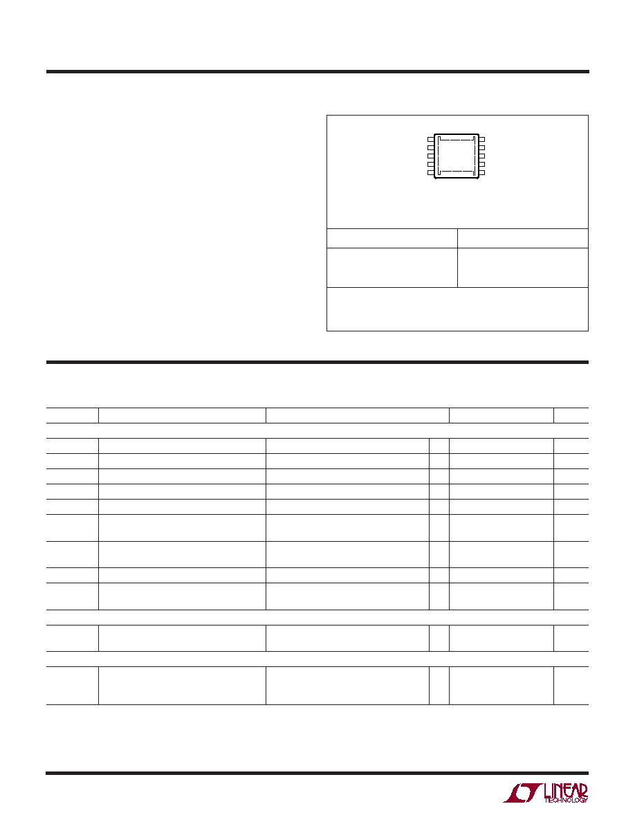
ORDER PART NUMBER
T
JMAX
= 125
°C,
JA
= 45
°C/W,
JC
= 10
°C/W
EXPOSED PAD (PIN 11) IS GND, MUST BE SOLDERED TO PCB
LTC3725EMSE
LTC3725IMSE
ABSOLUTE AXI U
RATI GS
W
W
W
U
PACKAGE/ORDER I FOR ATIO
U
U
W
(Note 1)
ELECTRICAL CHARACTERISTICS
The
denotes the specifications which apply over the full operating
temperature range, otherwise specifications are at T
A
= 25
°C. V
CC
= 12V, GND = PGND = 0V, T
A
= 25
°C, unless otherwise noted.
SYMBOL
PARAMETER
CONDITIONS
MIN
TYP
MAX
UNITS
V
CC
Supply, Linear Regulator and Trickle Charger Shunt Regulator
V
CCOP
Operating Voltage Range
7
12
15
V
V
CCLR
Output Voltage
Linear Regulator in Operation
8
V
I
NDRV
Current into NDRV Pin
Linear Regulator in Operation
0.1
1
mA
t
r(VCC)
Rise Time of V
CC
Linear Regulator Charging (0.5V to 7.5V)
45
µs
I
NDRVTO
Linear Regulator Time Out Current Threshold
Primary-Side Operation
0.27
mA
I
CC
Supply Current
V
UVLO
= 1.5V, Linear Regulator in
1.4
2.1
mA
Operation (Note 3)
I
CCM
Maximum Supply Current
V
UVLO
= 1.5V, Trickle Charger in Operation,
1.7
2.5
mA
V
CC
= 13.2V (Note 3)
V
CCSR
Maximum Supply Voltage
Trickle Charger Shunt Regulator
14.25
15
V
I
CCSR
Minimum Current into NDRV/V
CC
Trickle Charger Shunt Regulator, V
CC
= 15V
10
mA
(Note 3)
Internal Undervoltage
V
CCUV
Internal Undervoltage Threshold
V
CC
Rising
5.3
V
V
CC
Falling
4.7
V
Gate Drive Undervoltage
V
GDUV
Gate Drive Undervoltage Threshold
V
CC
Rising (Linear Regulator)
7.2
7.4
7.7
V
V
CC
Rising (Trickle Charger)
13.1
13.4
14
V
V
CC
Falling
6.8
7.0
7.2
V
MSE PART MARKING
1
2
3
4
5
UVLO
SSFLT
NDRV
FB/IN
+
FS/IN
10
9
8
7
6
I
S
V
SLMT
V
CC
GATE
PGND
TOP VIEW
11
MSE PACKAGE
10-LEAD PLASTIC MSOP
LTBSV
LTBSW
Order Options Tape and Reel: Add #TR
Lead Free: Add #PBF Lead Free Tape and Reel: Add #TRPBF
Lead Free Part Marking:
http://www.linear.com/leadfree/
Consult LTC Marketing for parts specified with wider operating temperature ranges.
LTC3725
3
3725f
The
denotes the specifications which apply over the full operating
temperature range, otherwise specifications are at T
A
= 25
°C. V
CC
= 12V, GND = PGND = 0V, T
A
= 25
°C, unless otherwise noted.
ELECTRICAL CHARACTERISTICS
SYMBOL
PARAMETER
CONDITIONS
MIN
TYP
MAX
UNITS
Undervoltage Lockout (UVLO)
V
UVLOR
Undervoltage Lockout Threshold Rising
Rising
1.220
1.242
1.280
V
V
UVLOF
Undervoltage Lockout Threshold Falling
Falling
1.205
1.226
1.265
V
I
HUVLO
Hysteresis Current
V
UVLO
= 1V
4.2
4.9
5.6
µA
V
UVLOOP
Voltage Feedforward Operating Range
Primary-Side Control
V
UVLOF(MIN)
3.75
V
Gate Driver (GATE)
R
OS
Output Pull-Down Resistance
I
OUT
= 100mA
1.9
V
OH
High Output Voltage
I
OUT
= 100mA
11
V
I
PU
Peak Pull-Up Current
1.7
A
t
r
Output Rise Time
10% to 90%, C
OUT
= 4.7nF
40
ns
t
f
Output Fall Time
10% to 90%, C
OUT
= 4.7nF
70
ns
Rectifier
I
RECT
Maximum Rectifier DC Output Current
25
mA
Oscillator
f
OSC(P)
Oscillator Frequency
Primary-Side Control, R
FS(P)
= 100k
200
kHz
Primary-Side Control, R
FS(P)
= 25k
700
kHz
Primary-Side Control, R
FS(P)
= 300k
70
kHz
f
RFS(P)
Oscillator Resistor Set Accuracy
Primary-Side Control
25k < R
FSET
< 300k
±15
%
f
OSC(S)
Oscillator Frequency
Secondary-Side Control (During Start-Up),
300
kHz
R
FS(S)
= 100k
Soft-Start/Fault (SSFLT)
I
SS(C)
Soft-Start Charge Current
Primary-Side Control, V
SSFLT
= 2V
5.2
µA
Secondary-Side Control, V
UVLO
= 1.3V,
4
µA
V
SSFLT
= 2V
Secondary-Side Control, V
UVLO
= 3.75V,
1.6
µA
V
SSFLT
= 2V
V
LRTO
Linear Regulator Time Out-Threshold
3.9
V
V
FLTH
Fault Output High
V
CC
= 8V
6.7
V
I
SS(D)
Soft-Start Discharge Current
Timing Out After Fault, V
SSFLT
= 2V
1
µA
Current Sense Input (I
S
)
V
IS(MAX)
Overcurrent Threshold
300
mV
Volt Second Limit (V
SLMT
)
V
VSL(MAX)
Volt-Second Limit Threshold
1.26
V
I
VSLMT(MAX)
Maximum Volt-Second Limit Resistor Current
0.25
mA
Optoisolator Bias Current
V
OPTO
Open Circuit Optoisolator Voltage
Primary-Side Control I
FB
= 0V
3.3
V
I
OPTO
Optoisolator Bias Current
Primary-Side Control V
FB
= 2.5V
0.5
mA
Primary-Side Control V
FB
= 0V
1.6
mA
Note 1: Absolute Maximum Ratings are those values beyond which the life
of a device may be impaired.
Note 2: Operating junction temperature T
J
(in
°C) is calculated from the
ambient temperature T
A
and the average power dissipation PD (in watts)
by the formula: T
J
= T
A
+
JA
· PD. Refer to the Applications Information
section for details.
Note 3: I
CC
is the sum of current into NDRV and V
CC
.
LTC3725
4
3725f
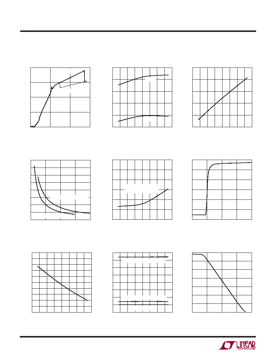
Supply Current vs V
CC
UVLO Voltage Threshold vs
Temperature
UVLO Hysteresis Current vs
Temperature
Oscillator Frequency
f
OSC
vs R
FSET
Oscillator Frequency vs
Temperature
Shunt Regulator Current I
CC
vs V
CC
Shunt Regulator Current vs
Temperature
V
GDUV
vs Temperature
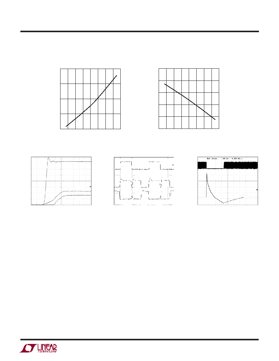
TYPICAL PERFOR A CE CHARACTERISTICS
U
W
Optoisolator Bias V
FB/IN
+ vs
I
FB/IN
+
V
CC
(V)
0
CURRENT (mA)
1.0
1.5
15
3725 G01
0.5
0
10
5
2.0
TRICKLE CHARGER
LINEAR REGULATOR
TEMPERATURE (
°C)
60
UVLO THRESHOLD (V)
1.240
1.235
1.230
1.225
100
3725 G02
1.220
40
60
80
0
20
20
40
1.245
V
UVLOF
V
UVLOR
TEMPERATURE (
°C)
60
I
HUVLO
(
µ
A)
5.00
4.95
4.90
4.85
100
3725 G03
4.80
40
60
80
0
20
20
40
5.05
R
FSET
(k
)
0
f
OSC
(kHz)
300
200
100
400
300
200
100
3725 G04
0
800
700
400
500
600
SECONDARY-SIDE CONTROL
PRIMARY-SIDE CONTROL
TEMPERATURE (
°C)
60
OSCILLATOR FREQUENCY f
OSC(P)
(kHz)
202
201
200
199
100
3725 G05
197
198
40
60
80
0
20
20
40
203
PRIMARY-SIDE CONTROL
R
FS(P)
= 100k
V
CC
(V)
14.00
I
CC
(mA)
9
6
3
15.00
14.75
14.50
14.25
3725 G06
0
18
12
15
TEMPERATURE (
°C)
60
I
CCSR
(mA)
100
3725 G07
15
16
17
18
19
40
60
80
0
20
20
40
25
24
23
22
21
20
TEMPERATURE (
°C)
60
V
GDUV
(V)
100
3725 G08
6
7
8
40
60
80
0
20
20
40
14
13
12
11
10
9
V
CC
RISING (TRICKLE CHARGER)
V
CC
RISING (LINEAR REGULATOR)
V
CC
FALLING (BOTH)
I
FB/IN
+ (mA)
0
V
FB/IN
+ (V)
1.5
1.0
0.5
2.0
1.5
1.0
0.5
3725 G09
0
3.5
2.0
2.5
3.0
LTC3725
5
3725f
TYPICAL PERFOR A CE CHARACTERISTICS
U
W
Gate Drive Pull-Down Resistance
vs Temperature
Gate Drive Peak Pull-Up Current
vs Temperature
Linear Regulator Start-Up
Gate Drive Encoding
Fault Operation
TEMPERATURE (
°C)
60
GATE DRIVE RESISTANCE R
OS
(
)
2.25
2.00
1.75
100
3725 G10
1.50
40
60
80
0
20
20
40
2.50
TEMPERATURE (
°C)
60
I
PU
(A)
1.9
1.8
1.7
1.6
100
3725 G11
1.5
40
60
80
0
20
20
40
2.0
5V/DIV
25
µs/DIV
3725 G12
V
IN
NDRV
V
CC
10V/DIV
1
µs/DIV
3705 G13
GATE
FB/IN
FS/IN
2V/DIV
10V/DIV
40ms/DIV
3725 G14
GATE
SSFLT