Äîêóìåíòàöèÿ è îïèñàíèÿ www.docs.chipfind.ru
1
LTC3737
3737f
Dual 2-Phase, No R
SENSE
TM
,
DC/DC Controller with
Output Tracking
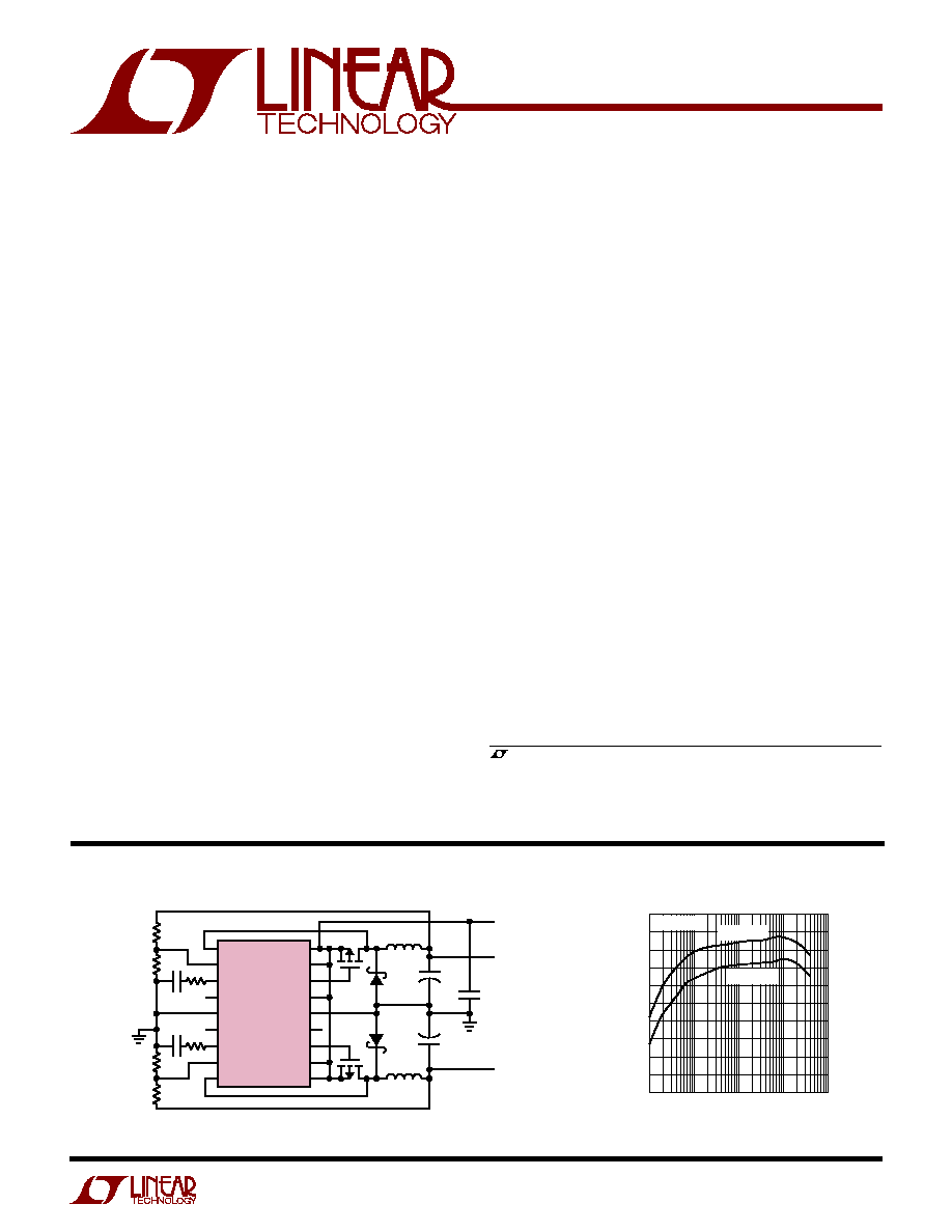
Figure 1. High Efficiency, 2-Phase, 550kHz Dual Step-Down Converter
s
Sense Resistor Optional
s
Out-of-Phase Controllers Reduce Required
Input Capacitance
s
Programmable Output Voltage Tracking
s
Constant Frequency Current Mode Architecture
s
Wide V
IN
Range: 2.75V to 9.8V
s
Wide V
OUT
Range: 0.6V to V
IN
s
0.6V
±
1.5% Reference
s
Low Dropout Operation: 100% Duty Cycle
s
True PLL for Frequency Locking or Adjustment
(Frequency Range 250kHz to 850kHz)
s
Selectable Burst Mode
®
or Pulse Skipping Operation
at Light Loads
s
Internal Soft-Start Circuitry
s
Selectable Maximum Peak Current Sense Threshold
s
Power Good Output Voltage Monitor
s
Output Overvoltage Protection
s
Micropower Shutdown: I
Q
= 9
µ
A
s
Tiny 4mm
×
4mm QFN and 24-Lead SSOP Packages
s
One or Two Lithium-Ion Powered Devices
s
Notebook and Palmtop Computers, PDAs
s
Portable Instruments
s
Distributed DC Power Systems
The LTC
®
3737 is a 2-phase dual step-down switching
regulator controller that requires few external compo-
nents. The constant frequency current mode architecture
provides excellent AC and DC load and line regulation.
MOSFET V
DS
sensing eliminates the need for current
sense resistors and improves efficiency. Power loss and
noise due to the ESR of the input capacitance are mini-
mized by operating the two controllers out of phase.
Burst Mode operation provides high efficiency operation
at light loads. 100% duty cycle provides low dropout
operation and extends battery operating time.
Switching frequency can be programmed up to 750kHz,
allowing the use of small surface mount inductors and
capacitors. For noise sensitive applications, the LTC3737
can be externally synchronized from 250kHz to 850kHz.
Other features include a power good output voltage moni-
tor, a tracking input and internal soft-start.
The LTC3737 is available in the low profile thermally
enhanced (4mm
×
4mm) QFN package or a 24-lead SSOP
narrow package.
+
+
SW1
V
FB1
I
TH1
PGOOD
SGND
TRACK
I
TH2
V
FB2
SW2
SENSE1
+
PV
IN1
PGATE1
V
IN
PGND
RUN/SS
PGATE2
PV
IN2
SENSE2
+
LTC3737
15k
M1
2.2
µ
H
2.2
µ
H
M2
D1
47
µ
F
10
µ
F
×
2
V
IN
2.75V TO
9.8V
V
OUT1
2.5V
V
OUT2
1.8V
47
µ
F
3737 F01
D2
59k
187k
59k
118k
15k
220pF
220pF
, LTC and LT are registered trademarks of Linear Technology Corporation.
Burst Mode is a registered trademark of Linear Technology Corporation.
No R
SENSE
is a trademark of Linear Technology Corporation.
U.S. patent numbers 5481178, 5731694, 5929620, 6144194,6580258, 5994885
DESCRIPTIO
U
FEATURES
APPLICATIO S
U
TYPICAL APPLICATIO
U
LOAD CURRENT (mA)
50
EFFICIENCY (%)
60
70
80
90
1
100
1000
10000
3737 F01b
10
100
55
65
75
85
95
V
IN
= 3.3V
V
OUT
= 2.5V
V
OUT
= 1.8V
Efficiency vs Load Current
2
LTC3737
3737f
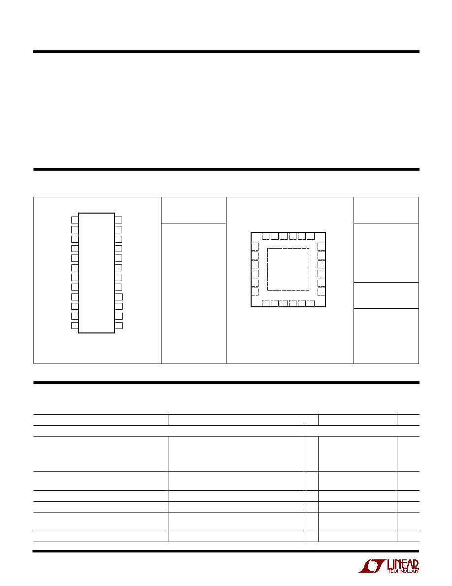
24 23 22 21 20 19
7
8
9
TOP VIEW
25
UF PACKAGE
24-LEAD (4mm
×
4mm) PLASTIC QFN
10 11 12
6
5
4
3
2
1
13
14
15
16
17
18
I
TH1
IPRG2
PLLLPF
SGND
V
IN
TRACK
PGATE1
PGND
PGATE2
RUN/SS
NC
V
FB1
IPRG1
SENSE1
+
PV
IN1
NC
V
FB2
I
TH2
PGOOD
SENSE2
+
PV
IN2
SW1
(SENSE1
)
SW2
(SENSE2
)
SYNC/
MODE
Input Supply Voltage (V
IN
), PV
IN1
, PV
IN2
,
SENSE1
+
, SENSE2
+
.................................. 0.3V to 10V
PGATE1, PGATE2, PLLLPF, RUN/SS, SYNC/MODE,
TRACK, IPRG1, IPRG2 Voltages .... 0.3V to (V
IN
+ 0.3V)
V
FB1
, V
FB2
, I
TH1
, I
TH2
Voltages .................. 0.3V to 2.4V
SW1, SW2 Voltages ............ 2V to V
IN
+ 1V or 10V Max
PGOOD ..................................................... 0.3V to 10V
PGATE1, PGATE2 Peak Output Current (<10
µ
s) ......... 1A
ABSOLUTE AXI U RATI GS
W
W
W
U
PACKAGE/ORDER I FOR ATIO
U
U
W
T
JMAX
= 125
°
C,
JA
= 130
°
C/W
ORDER PART
NUMBER
LTC3737EGN
Consult LTC Marketing for parts specified with wider operating temperature ranges.
Operating Temperature Range (Note 2) ... 40
°
C to 85
°
C
Storage Ambient Temperature Range
QFN Package .................................... 65
°
C to 125
°
C
SSOP Package .................................. 65
°
C to 150
°
C
Junction Temperature (Note 3) ............................ 125
°
C
Lead Temperature (Soldering, 10sec)
LTC3737EGN ................................................... 300
°
C
(Note 1)
ORDER PART
NUMBER
3737
LTC3737EUF
UF PART
MARKING
T
JMAX
= 125
°
C,
JA
= 37
°
C/W
EXPOSED PAD IS PGND (PIN 25) MUST BE SOLDERED TO PCB
1
2
3
4
5
6
7
8
9
10
11
12
TOP VIEW
SW1
(SENSE1
)
SW2
(SENSE2
)
GN PACKAGE
24-LEAD (NARROW) PLASTIC SSOP
24
23
22
21
20
19
18
17
16
15
14
13
IPRG1
V
FB1
I
TH1
IPRG2
PLLLPF
SGND
V
IN
TRACK
V
FB2
I
TH2
PGOOD
SENSE1
+
PV
IN1
NC
SYNC/MODE
PGATE1
PGND
PGATE2
RUN/SS
NC
PV
IN2
SENSE2
+
ELECTRICAL CHARACTERISTICS
The
q
denotes specifications that apply over the full operating temperature
range, otherwise specifications are at T
A
= 25
°
C. V
IN
= 4.2V unless otherwise specified.
PARAMETER
CONDITIONS
MIN
TYP
MAX
UNITS
Main Control Loops
Input DC Supply Current
(Note 4)
Sleep Mode
220
325
µ
A
Shutdown
RUN/SS = 0V
9
20
µ
A
UVLO
V
IN
< UVLO Threshold
3
10
µ
A
Undervoltage Lockout Threshold
V
IN
Falling
q
1.95
2.25
2.55
V
V
IN
Rising
q
2.15
2.45
2.75
V
Shutdown Threshold at RUN/SS
0.45
0.65
0.85
V
Start-Up Current Source
RUN/SS = 0V
0.5
0.7
1
µ
A
Regulated Feedback Voltage
0
°
C to 85
°
C (Note 5)
0.591
0.6
0.609
V
40
°
C to 85
°
C
q
0.588
0.6
0.612
V
Output Voltage Line Regulation
2.75V < V
IN
< 9.8V (Note 5)
0.05
0.2
mV/V
3
LTC3737
3737f
ELECTRICAL CHARACTERISTICS
The
q
denotes specifications that apply over the full operating temperature
range, otherwise specifications are at T
A
= 25
°
C. V
IN
= 4.2V unless otherwise specified.
Note 1: Absolute Maximum Ratings are those values beyond which the life
of a device may be impaired.
Note 2: The LTC3737E is guaranteed to meet specified performance from
0
°
C to 70
°
C. Specifications over the 40
°
C to 85
°
C operating range are
assured by design, characterization and correlation with statistical process
controls.
Note 3: T
J
is calculated from the ambient temperature T
A
and power
dissipation P
D
according to the following formula:
T
J
= T
A
+ (P
D
·
JA
°
C/W)
Note 4: Dynamic supply current is higher due to gate charge being
delivered at the switching frequency.
Note 5: The LTC3737 is tested in a feedback loop that servos I
TH
to a
specified voltage and measures the resultant V
FB
voltage.
Note 6: Peak current sense voltage is reduced dependent on duty cycle to
a percentage of value as shown in Figure 2.
PARAMETER
CONDITIONS
MIN
TYP
MAX
UNITS
Output Voltage Load Regulation
I
TH
= 0.9V (Note 5)
0.12
0.5
%
I
TH
= 1.7V
0.12
0.5
%
V
FB1,2
Input Current
(Note 5)
10
50
nA
TRACK Input Current
TRACK = 0.6V
10
50
nA
Overvoltage Protect Threshold
Measured at V
FB
0.66
0.68
0.7
V
Overvoltage Protect Hysteresis
20
mV
Auxiliary Feedback Threshold
SYNC/MODE Ramping Negative
0.525
0.6
0.675
V
Gate Drive 1, 2 Rise Time
C
L
= 3000pF
40
ns
Gate Drive 1, 2 Fall Time
C
L
= 3000pF
40
ns
Maximum Current Sense Voltage
IPRG = Floating (Note 6)
q
110
125
140
mV
(SENSE
+
SW)(
V
SENSE(MAX)
)
IPRG = 0V (Note 6)
q
70
85
100
mV
IPRG = V
IN
(Note 6)
q
185
204
223
mV
Soft-Start Time
Time for V
FB1
to Ramp from 0.05V to 0.55V
0.667
0.833
1
ms
Oscillator and Phase-Locked Loop
Oscilator Frequency
Unsynchronized (SYNC/MODE Not Clocked)
V
PLLLPF
= Floating
q
480
550
600
kHz
V
PLLLPF
= 0V
q
260
300
340
kHz
V
PLLLPF
= V
IN
q
650
750
825
kHz
Phase-Locked Loop Lock Range
SYNC/MODE Clocked
Minimum Synchronizable Frequency
q
200
250
kHz
Maximum Synchronizable Frequency
q
850
1150
kHz
Phase Detector Output Current
Sinking
f
OSC
> f
SYNC/MODE
4
µ
A
Sourcing
f
OSC
< f
SYNC/MODE
4
µ
A
PGOOD Output
PGOOD Voltage Low
I
PGOOD
Sinking 1mA
125
mV
PGOOD Trip Level
V
FB
with Respect to Set Output Voltage
V
FB
< 0.6V, Ramping Positive
13
10.0
7
%
V
FB
< 0.6V, Ramping Negative
16
13.3
10
%
V
FB
> 0.6V, Ramping Negative
13
10.0
7
%
V
FB
> 0.6V, Ramping Positive
16
13.3
10
%
4
LTC3737
3737f
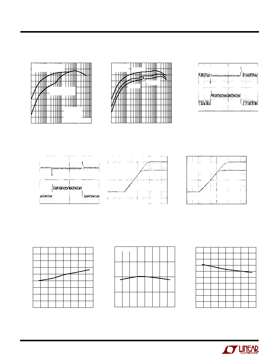
TYPICAL PERFOR A CE CHARACTERISTICS
U
W
Efficiency vs Load Current
LOAD CURRENT (mA)
50
EFFICIENCY (%)
60
70
80
90
1
100
1000
10000
3737 G01
10
100
55
65
75
85
95
Burst Mode OPERATION
(SYNC/MODE = V
IN
)
PULSE SKIPPING
(SYNC/MODE = 0V)
T
A
= 25
°
C
V
IN
= 3.3V
V
OUT
= 2.5V
FIGURE 13 CIRCUIT
LOAD CURRENT (mA)
65
EFFICIENCY (%)
95
100
60
55
90
75
85
80
70
1
100
1000
10000
3737 G02
50
10
T
A
= 25
°
C
V
OUT
= 2.5V
V
IN
= 3.3V
V
IN
= 5V
V
IN
= 4.2V
V
OUT
AC-COUPLED
100mV/DIV
V
IN
= 3.3V
200
µ
s/DIV
3737 G03
V
OUT
= 1.8V
I
LOAD
= 300mA TO 3A
SYNC/MODE = V
IN
FIGURE 13 CIRCUIT
I
L
2A/DIV
Efficiency vs Load Current
Load Step (Burst Mode Operation)
Load Step (Pulse Skipping Mode)
Tracking Start-Up with Internal
Soft-Start (C
SS
= 0nF)
Tracking Start-Up with External
Soft-Start (C
SS
= 10nF)
V
OUT
AC-COUPLED
100mV/DIV
V
IN
= 3.3V
200
µ
s/DIV
3737 G04
V
OUT
= 1.8V
I
LOAD
= 300mA TO 3A
SYNC/MODE = 0V
FIGURE 13 CIRCUIT
I
L
2A/DIV
V
IN
= 4.2V
250
µ
s/DIV
3737 G05
R
LOAD1
= R
LOAD2
= 1
FIGURE 13 CIRCUIT
500mV/
DIV
V
OUT1
2.5V
V
OUT2
1.8V
V
IN
= 4.2V
2.5ms/DIV
3737 G06
R
LOAD1
= R
LOAD2
= 1
FIGURE 13 CIRCUIT
500mV/
DIV
V
OUT1
2.5V
V
OUT2
1.8V
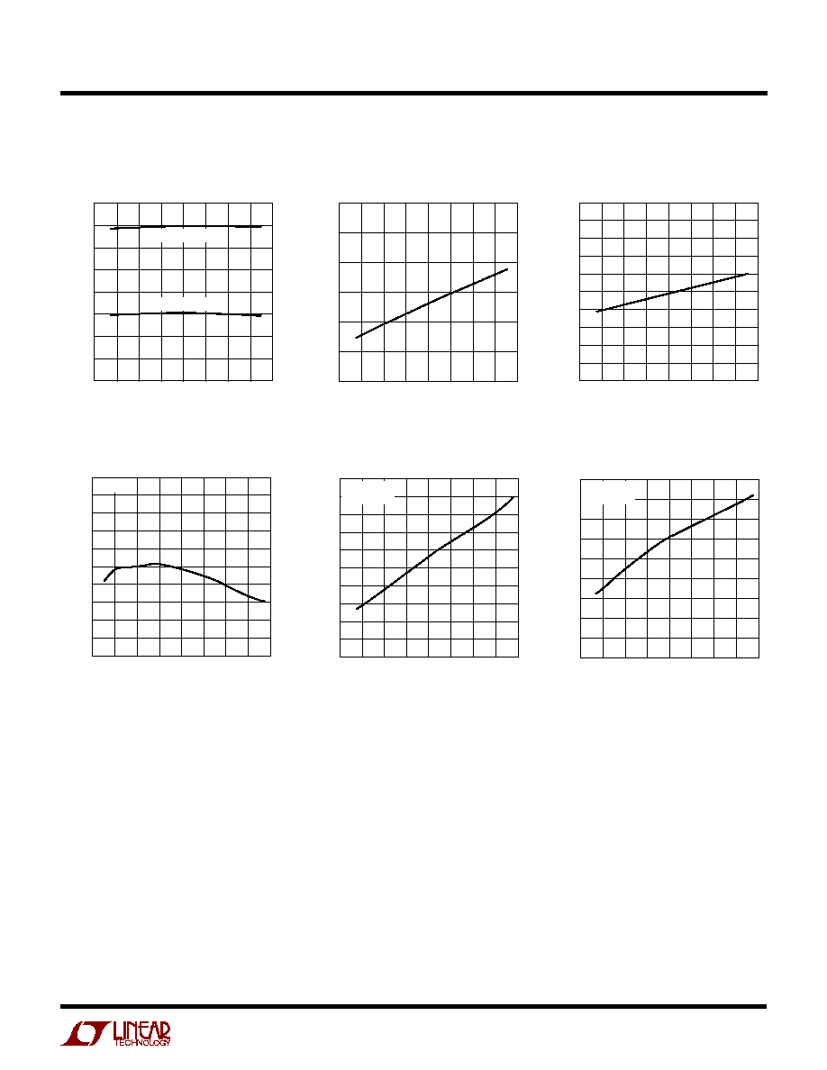
Regulated Feedback Voltage
vs Temperature
TEMPERATURE (
°
C)
60
FEEDBACK VOLTAGE (V)
0.601
0.603
0.605
100
3737 G07
0.599
0.597
0.591
20
20
60
40
0
40
80
0.595
0.593
0.609
0.607
TEMPERATURE (
°
C)
60
115
MAXIMUM CURRENT SENSE THRESHOLD (mV)
120
125
130
135
40 20
0
20
3737 G08
40
60
80
100
I
PRG
= FLOAT
TEMPERATURE (
°
C)
60
0
RUN/SS VOLTAGE (V)
0.1
0.3
0.4
0.5
1.0
0.7
20
20
40
3737 G09
0.2
0.8
0.9
0.6
40
0
60
80
100
Maximum Current Sense Threshold
vs Temperature
Shutdown (RUN) Threshold
vs Temperature
5
LTC3737
3737f
TYPICAL PERFOR A CE CHARACTERISTICS
U
W
Undervoltage Lockout Threshold
vs Temperature
TEMPERATURE (
°
C)
60
INPUT (V
IN
) VOLTAGE (V) 2.30
2.40
100
3737 G10
2.20
2.10
20
20
60
40
0
40
80
2.50
2.25
2.35
2.15
2.45
V
IN
RISING
V
IN
FALLING
TEMPERATURE (
°
C)
60
0.4
RUN/SS PULL-UP CURRENT (
µ
A)
0.5
0.6
0.7
0.8
20
20
60
100
3737 G11
0.9
1.0
40
0
40
80
TEMPERATURE (
°
C)
60
10
NROMALIZED FREQUENCY (%)
8
4
2
0
10
4
20
20
40
3737 G12
6
6
8
2
40
0
60
80
100
RUN/SS Pull-Up Current
vs Temperature
Oscillator Frequency
vs Temperature
Oscillator Frequency
vs Input Voltage
Shutdown Quiescent Current
vs Input Voltage
RUN/SS Start-Up Current
vs Input Voltage
INPUT VOLTAGE (V)
2
5
NORMALIZED FREQUENCY SHIFT (%)
4
2
1
0
5
2
4
6
7
3737 G13
3
3
4
1
3
5
8
9
10
T
A
= 25
°
C
INPUT VOLTAGE (V)
2
0
SHUTDOWN CURRENT (
µ
A)
2
6
8
10
20
14
4
6
7
3737 G14
4
16
18
12
3
5
8
9
10
T
A
= 25
°
C
RUN/SS = 0V
INPUT VOLTAGE (V)
2
RUN/SS PIN START-UP CURRENT (
µ
A)
0.5
0.6
0.7
10
3737 G15
0.4
0.3
0
0.1
4
6
8
3
5
7
9
0.2
0.9
0.8
T
A
= 25
°
C
RUN/SS = 0V