 | ÐлекÑÑоннÑй компоненÑ: LTC3827 | СкаÑаÑÑ:  PDF PDF  ZIP ZIP |
3827f
1
LTC3827
3827f
Low I
Q
, Dual, 2-Phase
Synchronous Controller
High Efficiency Dual 8.5V/3.3V Step-Down Converter
Wide Output Voltage Range: 0.8V
V
OUT
10V
Low Operating I
Q
: 80
µA (One Channel On)
Out-of-Phase Controllers Reduce Required Input
Capacitance and Power Supply Induced Noise
OPTI-LOOP
®
Compensation Minimizes C
OUT
±1% Output Voltage Accuracy
Wide V
IN
Range: 4V to 36V Operation
Phase-Lockable Fixed Frequency 140kHz to 650kHz
Selectable Continuous, Pulse Skipping or Low Ripple
Burst Mode
®
Operation at Light Loads
Dual N-Channel MOSFET Synchronous Drive
Very Low Dropout Operation: 99% Duty Cycle
Adjustable Output Voltage Soft-Start or Tracking
Output Current Foldback Limiting
Power Good Output Voltage Monitor
Output Overvoltage Protection
Low Shutdown I
Q
: 8
µA
Internal LDO Powers Gate Drive from V
IN
or V
OUT
Small 5mm
× 5mm QFN Package
The LTC
®
3827 is a high performance dual step-down
switching regulator controller that drives all N-channel
synchronous power MOSFET stages. A constant fre-
quency current mode architecture allows a phase-lock-
able frequency of up to 650kHz. Power loss and noise due
to the ESR of the input capacitor ESR are minimized by
operating the two controller output stages out of phase.
The 80
µA no-load quiescent current extends operating life
in battery powered systems. OPTI-LOOP compensation al-
lows the transient response to be optimized over a wide
range of output capacitance and ESR values. The LTC3827
features a precision 0.8V reference and a power good output
indicator. A wide 4V to 36V input supply range encom-
passes all battery chemistries.
Independent TRACK/SS pins for each controller ramp the
output voltage during start-up. Current foldback limits
MOSFET heat dissipation during short-circuit conditions.
The PLLIN/MODE pin selects among Burst Mode opera-
tion, pulse skipping mode, or continuous inductor current
mode at light loads. For a leaded package version
(28-lead SSOP), see the LTC3827-1 datasheet.
Automotive Systems
Battery-Operated Digital Devices
Distributed DC Power Systems
DESCRIPTIO
U
FEATURES
APPLICATIO S
U
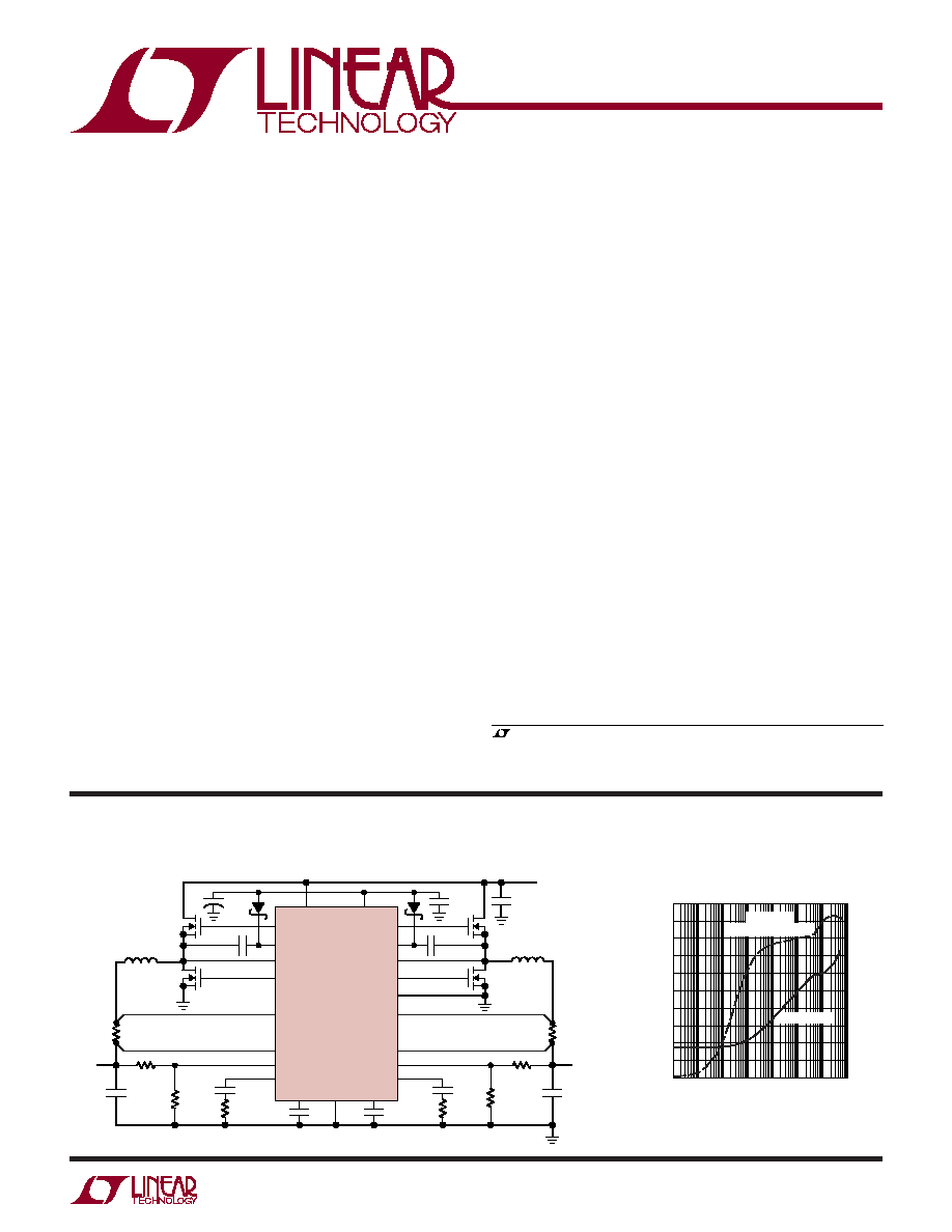
TYPICAL APPLICATIO
U
Efficiency and Power Loss
vs Load Current
+
4.7
µF
0.1
µF
62.5k
3.3
µH
220pF
150
µF
1
µF
22
µF
50V
0.015
20k
15k
V
OUT1
3.3V
5A
150
µF
0.1
µF
192.5k
7.2
µH
220pF
0.015
20k
15k
V
OUT2
8.5V
3.5A
TG1
TG2
BOOST1
BOOST2
SW1
SW2
BG1
BG2
SGND
PGND
SENSE1
+
SENSE2
+
SENSE1
SENSE2
V
FB1
V
FB2
I
TH1
I
TH2
V
IN
INTV
CC
TRACK/SS1
TRACK/SS2
V
IN
4V TO 36V
3827 TA01
0.1
µF
0.1
µF
LTC3827
LOAD CURRENT (mA)
EFFICIENCY (%)
POWER LOSS (mW)
0.01
0.1
1
10
100
1000 10000
3827 TA01b
0.001
1
10
1000
100
0.1
100000
10000
40
50
60
70
80
30
20
10
0
90
100
POWER LOSS
EFFICIENCY
V
IN
= 12V; V
OUT
= 3.3V
, LTC and LT are registered trademarks of Linear Technology Corporation. Burst Mode
and
OPTI-LOOP are
registered trademarks of Linear Technology Corporation. All other
trademarks are the property of their respective owners. Protected by U.S. Patents, including
5481178, 5929620, 6177787, 6144194, 6100678, 5408150, 6580258, 6304066, 5705919.
FIGURE 13 CIRCUIT
2
LTC3827
3827f
The
denotes the specifications which apply over the full operating
temperature range, otherwise specifications are at T
A
= 25
°C. V
IN
= 12V, V
RUN/SS1, 2
= 5V unless otherwise noted.
ELECTRICAL CHARACTERISTICS
Input Supply Voltage (V
IN
) .........................36V to 0.3V
Top Side Driver Voltages
(BOOST1, BOOST2) ...............................42V to 0.3V
Switch Voltage (SW1, SW2) .........................36V to 5V
(BOOST1-SW1), (BOOST2-SW2) ............... 8.5V to 0.3V
RUN1, RUN2 .............................................. 7V to 0.3V
SENSE1
+
, SENSE2
+
, SENSE1
,
SENSE2
Voltages ................................11V to 0.3V
PLLIN/MODE, PLLLPF, Voltages ......... INTV
CC
to 0.3V
PHASMD, FOLDDIS, TRACK/SS1, TRACK/SS2
Voltages .......................................... INTV
CC
to 0.3V
EXTV
CC
......................................................10V to 0.3V
I
TH1,
I
TH2
, V
FB1
, V
FB2
Voltages .................. 2.7V to 0.3V
PGOOD1, PGOOD2 Voltages ..................... 8.5V to 0.3V
Peak Output Current <10
µs (TG1, TG2, BG1, BG2) ... 3A
INTV
CC
Peak Output Current ................................ 50mA
Operating Temperature Range (Note 2) .. 40
°C to 85°C
Junction Temperature (Note 3) ............................. 125
°C
Storage Temperature Range ................. 65
°C to 125°C
ABSOLUTE AXI U RATI GS
W
W
W
U
(Note 1)
Order Options Tape and Reel: Add #TR
Lead Free: Add #PBF Lead Free Tape and Reel: Add #TRPBF
Lead Free Part Marking:
http://www.linear.com/leadfree/
Consult LTC Marketing for parts specified with wider operating temperature ranges.
PACKAGE/ORDER I FOR ATIO
U
U
W
LTC3827EUH
ORDER PART NUMBER
UH PART MARKING
3827
32 31 30 29 28 27 26 25
9
10 11 12 13 14 15 16
17
18
19
20
21
22
23
24
8
7
6
5
4
3
2
1
TOP VIEW
SENSE1
PLLLPF
PHASMD
CLKOUT
PLLIN/MODE
SGND
RUN1
RUN2
BOOST1
BG1
V
IN
PGND
EXTV
CC
INTV
CC
BG2
BOOST2
SENSE1
+
V
FB1
I
TH1
TRACK/SS1
PGOOD2
PGOOD1
TG1
SW1
SENSE2
SENSE2
+
V
FB2
I
TH2
TRACK/SS2
FOLDDIS
TG2
SW2
UH PACKAGE
32-LEAD (5mm
× 5mm) PLASTIC QFN
33
T
JMAX
= 125
°C,
JA
= 34
°C/W
EXPOSED PAD (PIN 33) IS SGND
MUST BE SOLDERED TO PCB
SYMBOL
PARAMETER
CONDITIONS
MIN
TYP
MAX
UNITS
Main Control Loops
V
FB1, 2
Regulated Feedback Voltage
(Note 4); I
TH1, 2
Voltage = 1.2V
0.792
0.800
0.808
V
I
VFB1, 2
Feedback Current
(Note 4)
5
50
nA
V
REFLNREG
Reference Voltage Line Regulation
V
IN
= 4V to 30V (Note 4)
0.002
0.02
%/V
V
LOADREG
Output Voltage Load Regulation
(Note 4)
Measured in Servo Loop;
I
TH
Voltage = 1.2V to 0.7V
0.1
0.5
%
Measured in Servo Loop;
I
TH
Voltage = 1.2V to 2V
0.1
0.5
%
g
m1, 2
Transconductance Amplifier g
m
I
TH1, 2
= 1.2V; Sink/Source 5
µA (Note 4)
1.55
mmho
I
Q
Input DC Supply Current
(Note 5)
Sleep Mode (Channel 1 On)
RUN1 = 5V, RUN2 = 0V, V
FB1
= 0.83V (No Load)
80
125
µA
Sleep Mode (Channel 2 On)
RUN1 = OV, RUN2 = 5V, V
FB2
= 0.83V (No Load)
80
125
µA
Shutdown
V
RUN1, 2
= 0V
8
20
µA
Sleep Mode (Both Channels)
RUN1,2 = 5V, V
FB1
= V
FB2
= 0.83V
115
160
µA
UVLO
Undervoltage Lockout
V
IN
Ramping Down
3.5
4
V
V
OVL
Feedback Overvoltage Lockout
Measured at V
FB1, 2
, Relative to Regulated V
FB1, 2
8
10
12
%
I
SENSE
Sense Pins Total Source Current
(Each Channel) V
SENSE1
, 2
= V
SENSE1
+
, 2
+
= 0V
660
µA
DF
MAX
Maximum Duty Factor
In Dropout
98
99.4
%
3
LTC3827
3827f
Note 1: Absolute Maximum Ratings are those values beyond which the life
of a device may be impaired.
Note 2: The LTC3827E is guaranteed to meet performance specifications
from 0
°C to 70°C. Specifications over the 40°C to 85°C operating
temperature range are assured by design, characterization and correlation
with statistical process controls.
Note 3: T
J
is calculated from the ambient temperature T
A
and power
dissipation P
D
according to the following formulas:
T
J
= T
A
+ (P
D
· 34
°C/W)
Note 4: The LTC3827 is tested in a feedback loop that servos V
ITH1, 2
to a
specified voltage and measures the resultant V
FB1, 2.
Note 5: Dynamic supply current is higher due to the gate charge being
delivered at the switching frequency. See Applications Information.
Note 6: Rise and fall times are measured using 10% and 90% levels. Delay
times are measured using 50% levels.
Note 7: The minimum on-time condition is specified for an inductor
peak-to-peak ripple current
40% of I
MAX
(see minimum on-time
considerations in the Applications Information section).
The
denotes the specifications which apply over the full operating
temperature range, otherwise specifications are at T
A
= 25
°C. V
IN
= 12V, V
RUN/SS1, 2
= 5V unless otherwise noted.
ELECTRICAL CHARACTERISTICS
SYMBOL
PARAMETER
CONDITIONS
MIN
TYP
MAX
UNITS
I
TRACK/SS1, 2
Soft-Start Charge Current
V
TRACK1, 2
= 0V
0.75
1.0
1.35
µA
V
RUN1, 2
ON
RUN Pin ON Threshold
V
RUN1,
V
RUN2
Rising
0.5
0.7
0.9
V
V
SENSE(MAX)
Maximum Current Sense Threshold
V
FB1, 2
= 0.7V,V
SENSE1, 2
= 3.3V
90
100
110
mV
V
FB1, 2
= 0.7V,V
SENSE1, 2
= 3.3V
80
100
115
mV
TG Transition Time:
(Note 6)
TG1, 2 t
r
Rise Time
C
LOAD
= 3300pF
50
90
ns
TG1, 2 t
f
Fall Time
C
LOAD
= 3300pF
50
90
ns
BG Transition Time:
(Note 6)
BG1, 2 t
r
Rise Time
C
LOAD
= 3300pF
40
90
ns
BG1, 2 t
f
Fall Time
C
LOAD
= 3300pF
40
80
ns
TG/BG t
1D
Top Gate Off to Bottom Gate On Delay C
LOAD
= 3300pF Each Driver
70
ns
Synchronous Switch-On Delay Time
BG/TG t
2D
Bottom Gate Off to Top Gate On Delay C
LOAD
= 3300pF Each Driver
70
ns
Top Switch-On Delay Time
t
ON(MIN)
Minimum On-Time
(Note 7)
180
ns
INTV
CC
Linear Regulator
V
INTVCCVIN
Internal V
CC
Voltage
8.5V < V
IN
< 30V, V
EXTVCC
= 0V
5.0
5.25
5.5
V
V
LDOVIN
INTV
CC
Load Regulation
I
CC
= 0mA to 20mA, V
EXTVCC
= 0V
0.2
1.0
%
V
INTVCCEXT
Internal V
CC
Voltage
V
EXTVCC
= 8.5V
7.2
7.5
7.8
V
V
LDOEXT
INTV
CC
Load Regulation
I
CC
= 0mA to 20mA, V
EXTVCC
= 8.5V
0.2
1.0
%
V
EXTVCC
EXTV
CC
Switchover Voltage
I
CC
= 20mA, EXTV
CC
Ramping Positive
4.5
4.7
V
V
LDOHYS
EXTV
CC
Hysteresis
0.2
V
Oscillator and Phase-Locked Loop
f
NOM
Nominal Frequency
V
PLLLPF
= Floating; PLLIN/MODE = DC Voltage
360
400
440
kHz
f
LOW
Lowest Frequency
V
PLLLPF
= 0V; PLLIN/MODE = DC Voltage
220
250
280
kHz
f
HIGH
Highest Frequency
V
PLLLPF
= INTV
CC
; PLLIN/MODE = DC Voltage
475
530
580
kHz
f
SYNCMIN
Minimum Synchronizable Frequency PLLIN/MODE = External Clock; V
PLLLPF
= 0V
115
140
kHz
f
SYNCMAX
Maximum Synchronizable Frequency PLLIN/MODE = External Clock; V
PLLLPF
= 2V
650
800
kHz
I
PLLLPF
Phase Detector Output Current
Sinking Capability
f
PLLIN/MODE
< f
OSC
5
µA
Sourcing Capability
f
PLLIN/MODE
> f
OSC
5
µA
PGOOD Output
V
PGL
PGOOD Voltage Low
I
PGOOD
= 2mA
0.1
0.3
V
I
PGOOD
PGOOD Leakage Current
V
PGOOD
= 5V
±1
µA
V
PG
PGOOD Trip Level
V
FB
with Respect to Set Regulated Voltage
V
FB
Ramping Negative
12
10
8
%
V
FB
Ramping Positive
8
10
12
%
4
LTC3827
3827f
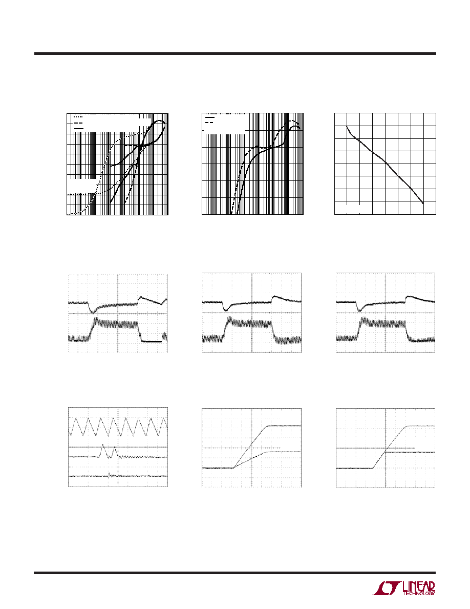
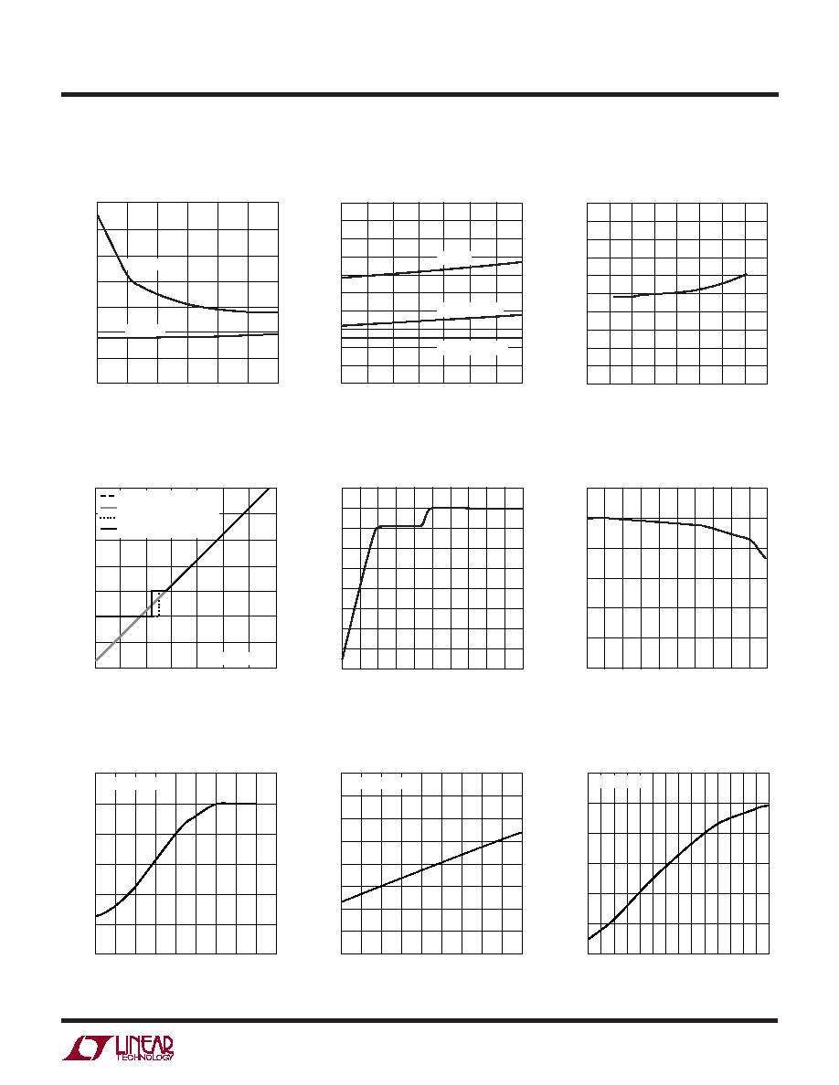
TYPICAL PERFOR A CE CHARACTERISTICS
U
W
Inductor Current at Light Load
Soft Start-Up
Tracking Start-Up
Load Step
(Burst Mode Operation)
Load Step
(Forced Continuous Mode)
Load Step
(Pulse Skip Mode)
Efficiency and Power Loss
vs Output Current
Efficiency vs Load Current
Efficiency vs Input Voltage
LOAD CURRENT (mA)
EFFICIENCY (%)
POWER LOSS (mW)
0.01
0.1
1
10
100
1000 10000
3827 G01
0.001
1
10
1000
100
0.1
10000
40
50
60
70
80
30
20
10
0
90
100
Burst Mode OPERATION
FORCED CONTINUOUS MODE
PULSE SKIPPING MODE
V
IN
= 12V
V
OUT
= 3.3V
LOAD CURRENT (mA)
EFFICIENCY (%)
0.01
0.1
1
10
100
1000 10000
3827 G02
0.001
50
60
70
80
40
90
100
V
IN
= 12V
V
IN
= 5V
V
OUT
= 3.3V
INPUT VOLTAGE (V)
EFFICIENCY (%)
5
10
15
20
30
40
3827 G03
0
25
35
86
88
90
92
94
84
82
96
98
V
OUT
= 3.3V
20
µs/DIV
V
OUT
100mV/DIV
AC
COUPLED
I
L
2A/DIV
3827 G04
20
µs/DIV
V
OUT
100mV/DIV
AC
COUPLED
I
L
2A/DIV
3827 G05
20
µs/DIV
V
OUT
100mV/DIV
AC
COUPLED
I
L
2A/DIV
3827 G06
4
µs/DIV
FORCED
CONTINUOUS
MODE
2A/DIV
BURST MODE
PULSE
SKIPPING
MODE
3827 G07
20ms/DIV
3827 G08
V
OUT2
2V/DIV
V
OUT1
2V/DIV
20ms/DIV
3827 G09
V
OUT2
2V/DIV
V
OUT1
2V/DIV
FIGURE 13 CIRCUIT
V
OUT
= 3.3V
I
LOAD
= 300
µA
FIGURE 13 CIRCUIT
FIGURE 13 CIRCUIT
FIGURE 13 CIRCUIT
V
OUT
= 3.3V
FIGURE 13 CIRCUIT
V
OUT
= 3.3V
FIGURE 13 CIRCUIT
V
OUT
= 3.3V
FIGURE 13 CIRCUIT
FIGURE 13 CIRCUIT
FFIGURE 13 CIRCUIT
5
LTC3827
3827f
TYPICAL PERFOR A CE CHARACTERISTICS
U
W
Foldback Current Limit
Quiescent Current vs Temperature
SENSE Pins Total Input
Bias Current vs I
TH
Maximum Current Sense Voltage
vs I
TH
Voltage
Sense Pins Total Input
Bias Current
Maximum Current Sense
Threshold vs Duty Cycle
I
TH
PIN VOLTAGE (V)
0
40
60
100
0.6
1.0
3827 G13
20
0
0.2
0.4
0.8
1.2
1.4
20
40
80
CURRENT SENSE THRESHOLD (mV)
PULSE SKIPPING
FORCED CONTINUOUS
BURST MODE (RISING)
BURST MODE (FALLING)
10% Duty Cycle
V
SENSE
COMMON MODE VOLTAGE (V)
0
700
INPUT CURRENT (
µ
A)
600
400
300
200
6
7
8
9
200
3827 G14
500
1
2
3
4
5
10
100
0
100
DUTY CYCLE (%)
0
CURRENT SENSE THRESHOLD (mV)
40
80
120
20
60
100
20
40
60
80
3827 G15
100
10
0
30
50
70
90
FEEDBACK VOLTAGE (V)
0
0
MAXIMUM CURRENT SENSE VOLTAGE (V)
20
60
80
100
0.2
0.4 0.5
0.9
3827 G16
40
0.1
0.3
0.6 0.7 0.8
120
TRACK/SS = 1V
TEMPERATURE (
°C)
45
QUIESCENT CURRENT (
µ
A)
80
85
90
75
3827 G17
75
70
60
15
15
45
30
90
0
30
60
65
100
95
PLLIN/MODE = 0V
I
TH
VOLTAGE (V)
0
INPUT CURRENT (
µ
A)
2
4
6
8
12
3827 G18
0
0.2
0.4
0.6
0.8
1.0
1.2
1.4
10
V
SENSE
= 3.3V
TEMPERATURE (
°C)
45
4.0
EXTV
CC
AND INTV
CC
VOLTAGES (V)
4.2
4.6
4.8
5.0
6.0
5.4
5
35
55
3827 G11
4.4
5.6
5.8
5.2
25
15
75
95
EXTV
CC
FALLING
EXTV
CC
RISING
INTV
CC
INPUT VOLTAGE (V)
0
5.00
INTV
CC
VOLTAGE (V)
5.05
5.15
5.20
5.25
5.50
5.35
10
20
25
3827 G12
5.10
5.40
5.45
5.30
5
15
30
35
40
INPUT VOLTAGE (V)
5
350
300
250
200
150
100
50
0
20
30
3827 G10
10
15
25
35
SUPPLY CURRENT (
µ
A)
300
µA LOAD
NO LOAD
Total Input Supply Current
vs Input Voltage
EXTV
CC
Switchover and INTV
CC
Voltages vs Temperature
INTV
CC
Line Regulation