 | ÐлекÑÑоннÑй компоненÑ: LTC3901 | СкаÑаÑÑ:  PDF PDF  ZIP ZIP |
Äîêóìåíòàöèÿ è îïèñàíèÿ www.docs.chipfind.ru
LTC3901
1
3901f
N-Channel Synchronous MOSFET Driver
Programmable Timeout
Reverse Inductor Current Sense
Gate Drive Transformer Synchronization
Sequence Monitor
Wide V
CC
Supply Range: 4.5V to 11V
15ns Rise/Fall Times at V
CC
= 5V, C
L
= 4700pF
Undervoltage Lockout
Small 16-Lead SSOP Package
Secondary Side
Synchronous Driver for Push-Pull
and Full-Bridge Converters
The LTC
®
3901 is a secondary side synchronous rectifier
driver designed to be used in isolated push-pull and full-
bridge converter power supplies. The chip drives two
external N-channel MOSFETs and accepts a transformer-
generated bipolar input to maintain sychronization with
the primary side controller.
The LTC3901 provides a full range of protection features
for the external MOSFETs. A programmable timeout func-
tion is included that disables both drivers when the syn-
chronization signal is missing or incorrect. Additionally,
the chip senses the output inductor current through the
drain-source resistance of the two MOSFETs, turning off
the MOSFETs if the inductor current reverses. The LTC3901
also shuts off the drivers if the supply is low or if the
synchronization sequence is incorrect.
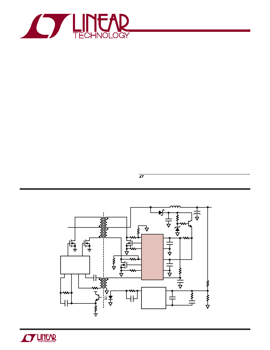
Figure 1. Simplified Isolated Push-Pull Converter
LTC3723
PUSH-PULL
CONTROLLER
LT4430 OR LT1431
OPTOCOUPLER
DRIVER
DRVA
DRVB
COMP V
FB
SDRB
SDRA
ISOLATION
BARRIER
T1
L1
CSE+
ME
CSE
CSF+
MF
CSF
V
CC
GND
PV
CC
PGND
LTC3901
OUT
T2
MA
MB
ME
MF
COMP
V
OUT
12V
C
OUT
V
IN
36V TO 72V
3901 F01
+
FB
SYNC
TIMER
48V Input Isolated DC/DC Converters
Isolated Telecom Power Supplies
Distributed Power Step-Down Converters
Industrial Control System Power Supplies
Automotive and Heavy Equipment
DESCRIPTIO
U
FEATURES
APPLICATIO S
U
TYPICAL APPLICATIO
U
, LTC and LT are registered trademarks of Linear Technology Corporation.
All other trademarks are the property of their respective owners.
LTC3901
2
3901f
The
denotes specifications which apply over the full operating
temperature range.
V
CC
= 5V, T
A
= 25
°
C unless otherwise specified. (Note 3)
Supply Voltage
V
CC
, PV
CC ............................................................................
12V
Input Voltage
CSE
, CSF
, TIMER ................. 0.3V to (V
CC
+ 0.3V)
SYNC ...................................................... 12V to 12V
Input Current
CSE
+
, CSF
+ .....................................................................
15mA
Operating Temperature Range (Note 2) ...40°C to 85°C
Storage Temperature Range ..................65°C to 150°C
Lead Temperature (Soldering, 10 sec).................. 300°C
ORDER PART
NUMBER
GN PART
MARKING
T
JMAX
= 125°C,
JA
= 130°C/W
3901
LTC3901EGN
ABSOLUTE AXI U
RATI GS
W
W
W
U
PACKAGE/ORDER I FOR ATIO
U
U
W
(Note 1)
ELECTRICAL CHARACTERISTICS
Consult LTC Marketing for parts specified with wider operating temperature ranges.
TOP VIEW
GN PACKAGE
16-LEAD NARROW PLASTIC SSOP
1
2
3
4
5
6
7
8
16
15
14
13
12
11
10
9
PV
CC
ME
ME
PGND
CSE
CSE
+
TIMER
GND
V
CC
MF
MF
PGND
CSF
CSF
+
GND
SYNC
SYMBOL
PARAMETER
CONDITIONS
MIN
TYP
MAX
UNITS
V
CC
Supply Voltage Range
4.5
5
11
V
V
UVLO
V
CC
Undervoltage Lockout Threshold
Rising Edge
4.1
4.5
V
V
CC
Undervoltage Lockout Hysteresis
Rising Edge to Falling Edge
0.5
V
I
VCC
V
CC
Supply Current
V
SYNC
= 0V
0.5
1
mA
f
SYNC
= 100kHz, C
ME
= C
MF
= 4700pF (Note 4)
7
15
mA
Timer
V
TMR
Timer Threshold Voltage
10%
V
CC
/5
10%
V
I
TMR
Timer Input Current
V
TMR
= 0V
6
10
µA
t
TMRDIS
Timer Discharge Time
C
TMR
= 1000pF, R
TMR
= 4.7k
40
120
ns
V
TMRMAX
Timer Pin Clamp Voltage
C
TMR
= 1000pF, R
TMR
= 4.7k
2.5
V
Current Sense (Note 5)
I
CS
+
CS
+
Input Current
V
CS
+ = 0V
±1
µA
I
CS
CS
Input Current
V
CS
= 0V
±1
µA
V
CSMAX
CS
+
Pin Clamp Voltage
I
IN
= 5mA, Driver Off
11
V
V
CS
Current Sense Threshold Voltage
V
CS
= 0V
7.5
10.5
13.5
mV
(Note 6)
3
18
mV
SYNC Input
I
SYNC
SYNC Input Current
V
SYNC
= ±10V
±1
±10
µA
V
SYNCP
SYNC Input Positive Threshold
1.0
1.4
1.8
V
SYNC Positive Input Hysteresis
(Note 7)
0.2
V
V
SYNCN
SYNC Input Negative Threshold
1.8
1.4
1.0
V
SYNC Negative Input Hysteresis
(Note 7)
0.2
V
Driver Output
R
ONH
Driver Pull-Up Resistance
I
OUT
= 100mA
0.9
1.2
1.6
R
ONL
Driver Pull-Down Resistance
I
OUT
= 100mA
0.8
1.2
1.6
I
PK
Driver Peak Output Current
(Note 7)
2
A
LTC3901
3
3901f
The
denotes specifications which apply over the full operating
temperature range.
V
CC
= 5V, T
A
= 25
°
C unless otherwise specified. (Note 3)
ELECTRICAL CHARACTERISTICS
TYPICAL PERFOR A CE CHARACTERISTICS
U
W
SYMBOL
PARAMETER
CONDITIONS
MIN
TYP
MAX
UNITS
Switching Characteristics (Note 8)
t
d
SYNC Input to Driver Output Delay
C
ME
= C
MF
= 4700pF, V
SYNC
= ±5V
60
120
ns
t
r
, t
f
Driver Rise/Fall Time
C
ME
= C
MF
= 4700pF, V
SYNC
= ±5V
15
ns
Note 1: Absolute Maximum Ratings are those values beyond which the life
of a device may be impaired.
Note 2: The LTC3901E is guaranteed to meet performance specifications
from 0°C to 70°C. Specifications over the 40°C to 85°C operating
temperature range are assured by design; characterization and correlation
with statistical process controls.
Note 3: All currents into device pins are positive; all currents out of device
pins are negative. All voltages are referenced to ground unless otherwise
specified.
Note 4: Supply current in normal operation is dominated by the current
needed to charge and discharge the external MOSFET gates. This current
will vary with supply voltage, switching frequency and the external
MOSFETs used.
Note 5: Both CSE
+
, CSE
and CSF
+
, CSF
current sense comparators have
the same performance specifications.
Note 6: The current sense comparator threshold has a 0.33%/°C
temperature coefficient (TC) to match the TC of the external MOSFET
R
DSON
.
Note 7: Guaranteed by design, not subject to test.
Note 8: Rise and fall times are measured using 10% and 90% levels. Delay
times are measured from ±1.4V at SYNC input to 20%/80% levels at the
driver output.
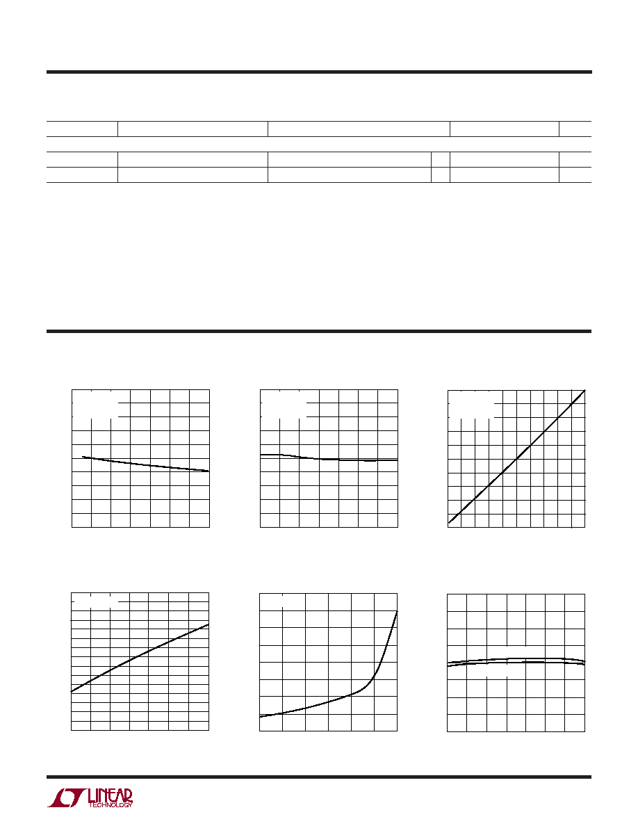
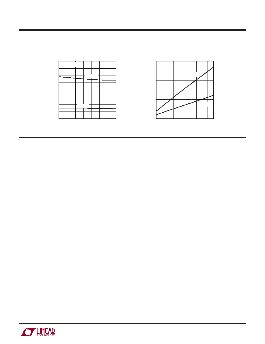
Timeout vs V
CC
Timeout vs Temperature
Timeout vs R
TMR
TIMEOUT (
µ
s)
5.25
5.20
5.15
5.10
5.05
5.00
4.95
4.90
4.85
4.80
4.75
V
CC
(V)
4
TIMEOUT (
µ
s)
5.25
5.20
5.15
5.10
5.05
5.00
4.95
4.90
4.85
4.80
4.75
6
8
9
3901 G01
5
7
10
11
TEMPERATURE (°C)
50
0
50
75
3901 G02
25
25
100
125
R
TMR
(k)
10
9
8
7
6
5
4
3
2
1
0
TIMEOUT (
µ
s)
3901 G03
0
10 20 30 40
50 60 70
80 90 100
T
A
= 25°C
R
TMR
= 51k
C
TMR
= 470pF
T
A
= 25°C
V
CC
= 5V
C
TMR
= 470pF
V
CC
= 5V
R
TMR
= 51k
C
TMR
= 470pF
CURRENT SENSE THRESHOLD (mV)
18
17
16
15
14
13
12
11
10
9
8
7
6
5
4
3
3901 G04
V
CC
= 5V, 11V
CS
+
INPUT CURRENT (mA)
0
5
V
CS(MAX)
CLAMP VOLTAGE (V)
10
20
15
25
30
3901 G05
18
17
16
15
14
13
12
11
10
TEMPERATURE (°C)
50
SYNC POSITIVE THRESHOLD (V)
100
3901 G06
0
50
1.8
1.7
1.6
1.5
1.4
1.3
1.2
1.1
1.0
25
25
75
125
TEMPERATURE (°C)
50
100
0
50
25
25
75
125
T
A
= 25°C
V
CC
= 5V
V
CC
= 11V
V
CS(MAX)
Clamp Voltage vs CS
+
Input Current
Current Sense Threshold vs
Temperature
SYNC Positive Threshold vs
Temperature
LTC3901
4
3901f
TYPICAL PERFOR A CE CHARACTERISTICS
U
W
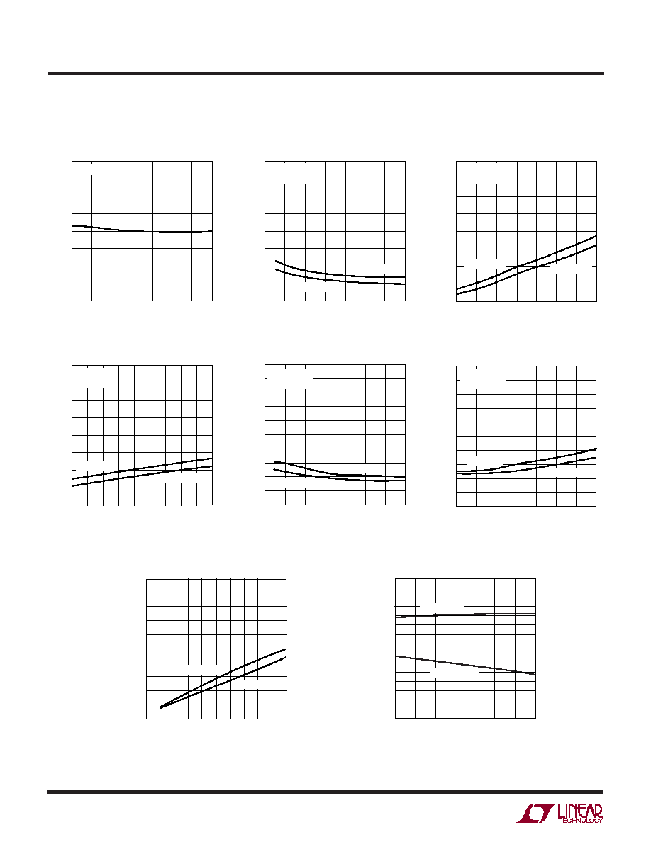
SYNC Negative Threshold vs
Temperature
Propagation Delay vs V
CC
Propagation Delay vs
Temperature
Propagation Delay vs C
LOAD
Rise/Fall Time vs V
CC
Rise/Fall Time vs Temperature
Rise/Fall Time vs Load
Capacitance
Undervoltage Lockout Threshold
Voltage vs Temperature
TEMPERATURE (°C)
50
SYNC NEGATIVE THRESHOLD (V)
100
3901 G07
0
50
1.0
1.1
1.2
1.3
1.4
1.5
1.6
1.7
1.8
25
25
75
125
V
CC
(V)
4
PROPAGATION DELAY (
µ
s)
10
3901 G08
6
8
120
110
100
90
80
70
60
50
40
5
7
9
11
TEMPERATURE (°C)
50
100
3901 G09
0
50
25
25
75
125
C
LOAD
(nF)
1
2
3
10
3901 G10
4
5
6
7
9
8
RISE/FALL TIME (ns)
50
45
40
35
30
25
20
15
10
5
0
RISE/FALL TIME (ns)
50
45
40
35
30
25
20
15
10
5
0
3901 G11
TEMPERATURE (°C)
3901 G12
T
A
= 25°C
C
LOAD
= 4.7nF
T
A
= 25°C
C
LOAD
= 4.7nF
T
A
= 25°C
V
CC
= 5V
V
CC
= 5V
C
LOAD
= 4.7nF
V
CC
= 5V
C
LOAD
= 4.7nF
V
CC
= 5V, 11V
SYNC TO ME
SYNC TO MF
SYNC TO ME
SYNC TO MF
SYNC TO ME
SYNC TO MF
PROPAGATION DELAY (
µ
s)
120
110
100
90
80
70
60
50
40
PROPAGATION DELAY (
µ
s)
120
110
100
90
80
70
60
50
40
V
CC
(V)
4
10
6
8
5
7
9
11
FALL TIME
FALL TIME
RISE TIME
RISE TIME
C
LOAD
(nF)
1
0
2
3
10
4
5
6
7
9
8
RISE/FALL TIME (ns)
50
45
40
35
30
25
20
15
10
5
0
T
A
= 25°C
V
CC
= 5V
FALL TIME
RISE TIME
UNDERVOLTAGE LOCKOUT THRESHOLD
VOLTAGE (V)
4.5
4.4
4.3
4.2
4.1
4.0
3.9
3.8
3.7
3.6
3.5
3.4
3.3
3.2
3.1
3.0
3901 G14
3901 G13
TEMPERATURE (°C)
50
100
0
50
25
25
75
125
FALLING EDGE
RISING EDGE
50
100
0
50
25
25
75
125
LTC3901
5
3901f
TYPICAL PERFOR A CE CHARACTERISTICS
U
W
V
CC
Supply Current
vs Load Capacitance
C
LOAD
(nF)
1
0
2
3
10
4
5
6
7
9
8
T
A
= 25°C
3901 G16
V
CC
= 5V
V
CC
= 11V
SUPPLY CURRENT (mA)
30
25
20
15
10
5
0
PVCC (Pin 1): Driver Supply Input. This pin powers the
ME and MF drivers. Bypass this pin to PGND using a 4.7µF
low ESR capacitor in close proximity to the LTC3901. This
pin should be connected to the same supply voltage as the
V
CC
pin.
ME (Pin 2, 3): Driver Output for ME. This pin drives the
gate of the external N-channel MOSFET, ME.
PGND (Pin 4,13): Power Ground. Both drivers return to
this pin. Connect PGND to a high current ground node in
close proximity to the sources of ME and MF.
CSE
+
, CSE
(Pin 6, 5): ME Current Sense Differential
Input. Connect CSE
+
through a series resistor to the drain
of ME and CSE
through a series resistor to the source of
ME. The LTC3901 monitors the CSE inputs 250ns after ME
goes high. If the inductor current reverses and flows into
ME causing CSE
+
to rise above CSE
by more than 10.5mV,
the LTC3901 pulls ME low. See the Current Sense section
for more details on choosing the resistance values for
R
CSE1
to R
CSE3
.
TIMER (Pin 7): Timer Input. Connect this pin to an external
R-C network to program the timeout period. The LTC3901
resets the timer at every positive and negative transition of
the SYNC input. If the SYNC signal is missing or incorrect,
the LTC3901 pulls both ME and MF low once the TIMER
pin goes above the timeout threshold. See the Timer sec-
tion for more details on programming the timeout period.
GND (Pin 8,10): Signal Ground. All internal low power
circuitry returns to this pin. To minimize differential ground
currents, connect GND to PGND right at the LTC3901.
SYNC (Pin 9): Driver Synchronization Input. 0V at this pin
forces both ME and MF high after an initial negative pulse.
A subsequent positive pulse at SYNC input forces ME to
pull low, whereas a negative pulse forces MF to pull low.
The SYNC signal should alternate between positive and
negative pulses. If the SYNC signal is incorrect, the LTC3901
pulls both MF and ME low.
CSF
+
, CSF
(Pin 11, 12): MF Current Sense Differential
Input. Connect CSF
+
through a series resistor to the drain
of MF and CSF
through a series resistor to the source of
MF. The LTC3901 monitors the CSF inputs 250ns after MF
goes high. If the inductor current reverses and flows into
MF causing CSF
+
to rise above CSF
by more than 10.5mV,
the LTC3901 pulls MF low. See the Current Sense section
for more details on choosing the resistance values for
R
CSF1
to R
CSF3
.
MF (Pin 14, 15): Driver Output for MF. This pin drives the
gate of the external N-channel MOSFET, MF.
V
CC
(Pin 16): Power Supply Input. All internal circuits
except the drivers are powered from this pin. Bypass this
pin to GND using a 1µF capacitor in close proximity to the
LTC3901.
U
U
U
PI FU CTIO S
V
CC
Supply Current vs
Temperature
3901 G15
TEMPERATURE (°C)
50
100
0
50
25
25
75
125
C
LOAD
= 4.7nF
V
CC
SUPPLY CURRENT (mA)
20
18
16
14
12
10
8
6
4
V
CC
= 5V
V
CC
= 11V