 | –≠–ª–µ–∫—Ç—Ä–æ–Ω–Ω—ã–π –∫–æ–º–ø–æ–Ω–µ–Ω—Ç: LTC4007 | –°–∫–∞—á–∞—Ç—å:  PDF PDF  ZIP ZIP |
1
LTC4007
4007i
4A, High Efficiency,
Standalone Li Battery Charger
January 2003
s
Complete Charger Controller for 3- or 4-Cell
Lithium-Ion Batteries
s
High Conversion Efficiency: Up to 96%
s
Output Currents Exceeding 4A
s
±
0.8% Charging Voltage Accuracy
s
Built-In Charge Termination for Li-Ion Batteries
s
AC Adapter Current Limiting Maximizes Charge Rate*
s
Thermistor Input for Temperature Qualified Charging
s
Wide Input Voltage Range: 6V to 28V
s
0.5V Dropout Voltage; Maximum Duty Cycle: 98%
s
Programmable Charge Current:
±
5% Accuracy
s
Indicator Outputs for Charging, C/10 Current
Detection, AC Adapter Present, Low Battery, Input
Current Limiting and Faults
s
Charging Current Monitor Output
s
Available in a 24-Pin Narrow SSOP Package
s
Notebook Computers
s
Portable Instruments
s
Battery-Backup Systems
s
Standalone Li-Ion Chargers
, LTC and LT are registered trademarks of Linear Technology Corporation.
FEATURES
DESCRIPTIO
N
U
APPLICATIO S
U
Final Electrical Specifications
Information furnished by Linear Technology Corporation is believed to be accurate and reliable.
However, no responsibility is assumed for its use. Linear Technology Corporation makes no represen-
tation that the interconnection of its circuits as described herein will not infringe on existing patent rights.
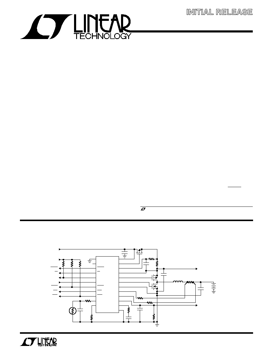
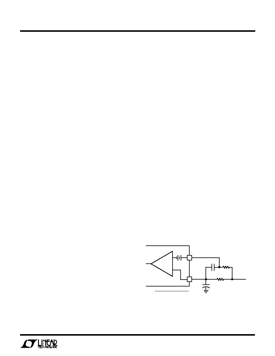
TYPICAL APPLICATIO
U
12.6V, 4A Li-Ion Battery Charger
The LTC
Æ
4007 is a complete constant-current/constant-
voltage charger controller for 3- or 4-cell lithium-ion
batteries. The PWM controller uses a synchronous, quasi-
constant frequency, constant off-time architecture that
will not generate audible noise even when using ceramic
capacitors. Charging current is programmable to
±
5%
accuracy using a programming resistor. Charging current
can also be monitored as a voltage across the program-
ming resistor.
The output float voltage is pin programmed for cell count
(3 cells or 4 cells) and chemistry (4.2V/4.1V). A timer,
programmed by an external resistor, sets the total charge
time. Charging is automatically restarted when cell voltage
falls below 3.9V/cell.
LTC4007 includes a thermistor input, which suspends
charging if an unsafe temperature condition is detected. If
the cell voltage is less than 2.5V, a low-battery indicator
asserts and can be used to program a trickle charge cur-
rent to safely charge depleted batteries. The FAULT pin is
also asserted and charging terminates if the low-battery
condition persists for more than 1/4 of the total charge time.
3C4C
CHEM
LOBAT
I
CL
ACP
SHDN
FAULT
CHG
FLAG
NTC
R
T
LOBAT
I
CL
ACP
SHDN
FAULT
CHG
FLAG
DCIN
INFET
CLP
CLN
TGATE
BGATE
PGND
CSP
BAT
PROG
ITH
GND
LTC4007
32.4k
309k
0.47
µ
F
THERMISTOR
10k
NTC
TIMING RESISTOR
(~2 HOURS)
100k
100k
100k
V
LOGIC
DCIN
0V TO 28V
0.1
µ
F
INPUT SWITCH
15nF
Q1
Q2
20
µ
F
10
µ
H
4.9k
3.01k
3.01k
0.025
0.025
20
µ
F
Li-Ion
BATTERY
CHARGING
CURRENT
MONITOR
Q1: Si4431DY
Q2: FDC6459
SYSTEM
LOAD
0.12
µ
F
6.04k
26.7k
0.0047
µ
F
4007 TA01
*U.S. Patent No. 5,723,970
2
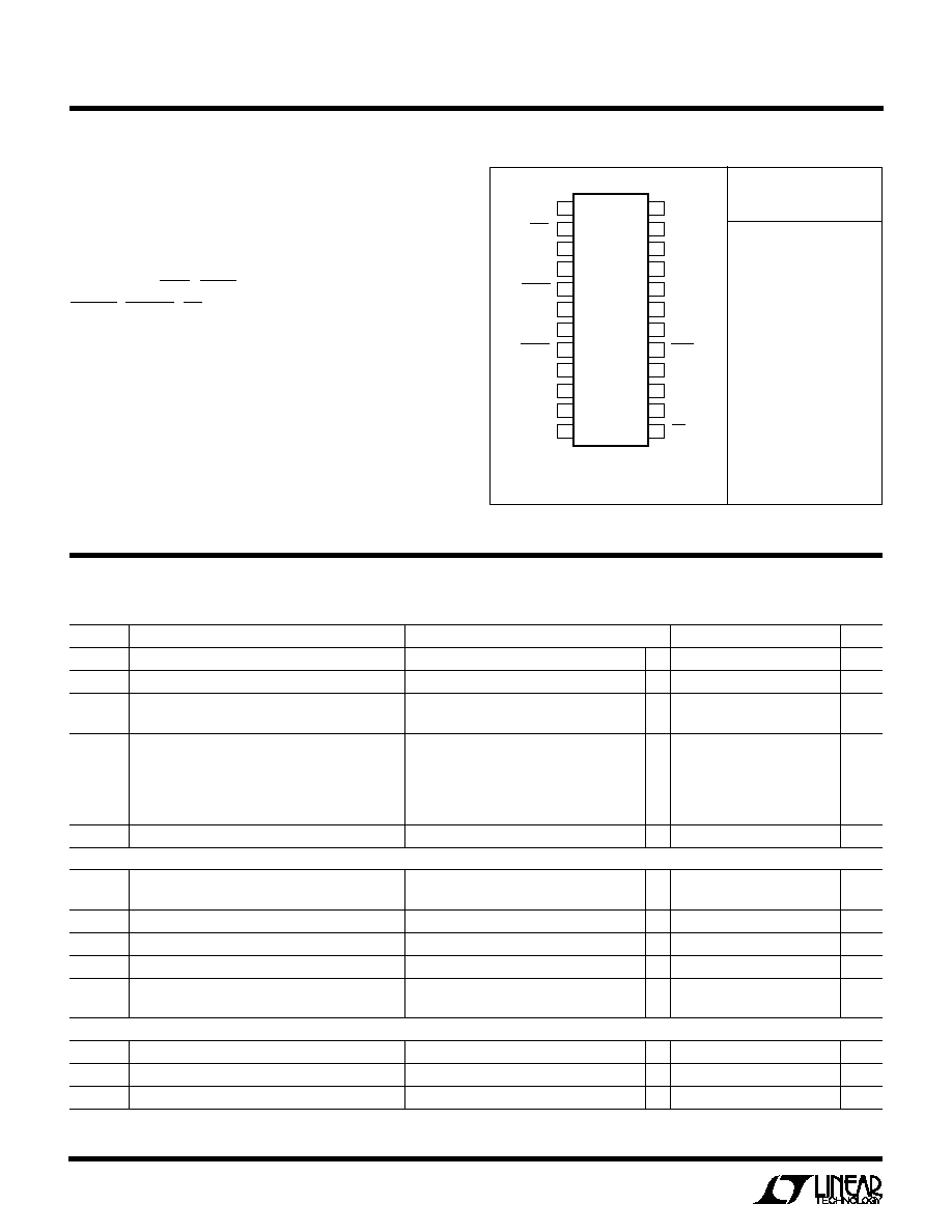
LTC4007
4007i
1
2
3
4
5
6
7
8
9
10
11
12
TOP VIEW
GN PACKAGE
24-LEAD PLASTIC SSOP
24
23
22
21
20
19
18
17
16
15
14
13
DCIN
CHG
ACP
R
T
FAULT
GND
3C4C
LOBAT
NTC
ITH
PROG
NC
SHDN
INFET
BGATE
PGND
TGATE
CLN
CLP
FLAG
CHEM
BAT
CSP
I
CL
(Note 1)
Voltage from DCIN, CLP, CLN to GND ....... + 32V/≠ 0.3V
PGND with Respect to GND .................................
±
0.3V
CSP, BAT to GND ....................................... +28V/≠ 0.3V
CHEM, 3C4C, R
T
to GND .............................. +7V/≠ 0.3V
NTC ............................................................ +10V/≠ 0.3V
ACP, SHDN, CHG, FLAG,
FAULT, LOBAT, I
CL ..............................................
+ 32V/≠ 0.3V
Operating Ambient Temperature Range
(Note 4) ............................................. ≠ 40
∞
C to 85
∞
C
Operating Junction Temperature ......... ≠ 40
∞
C to 125
∞
C
Storage Temperature Range ................. ≠ 65
∞
C to 150
∞
C
Lead Temperature (Soldering, 10 sec).................. 300
∞
C
ABSOLUTE
M
AXI
M
U
M
RATINGS
W
W
W
U
PACKAGE/ORDER I
N
FOR
M
ATIO
N
W
U
U
ORDER PART
NUMBER
LTC4007EGN
T
JMAX
= 125
∞
C,
JA
= 90
∞
C/W
The
q
denotes specifications which apply over the full operating
temperature range (Note 4), otherwise specifications are at T
A
= 25
∞
C. V
DCIN
= 20V, V
BAT
= 12V unless otherwise noted.
Consult LTC Marketing for parts specified with wider operating temperature ranges.
ELECTRICAL CHARACTERISTICS
SYMBOL
PARAMETER
CONDITIONS
MIN
TYP
MAX
UNITS
DCIN Operating Range
6
28
V
I
Q
Operating Current
Sum of Current from CLP, CLN , DCIN
3
5
mA
V
TOL
Charge Voltage Accuracy
Nominal Values: 12.3V, 12.6V, 16.4V, 16.8V
≠0.8
0.8
%
(Note 2)
q
≠1.0
1.0
%
I
TOL
Charge Current Accuracy (Note 3)
V
CSP
≠ V
BAT
Target = 100mV
≠ 4
4
%
q
≠ 5
5
%
V
BAT
< 6V, V
CSP
≠ V
BAT
Target = 10mV
≠60
60
%
6V
V
BAT
V
LOBAT
, V
CSP
≠ V
BAT
≠35
35
%
Target = 10mV
T
TOL
Termination Timer Accuracy
R
RT
= 270k
q
≠15
15
%
Shutdown
Battery Leakage Current
DCIN = 0V
q
15
30
µ
A
SHDN = 3V
q
≠10
10
µ
A
UVLO
Undervoltage Lockout Threshold
DCIN Rising, V
BAT
= 0
q
4.2
4.7
5.5
V
Shutdown Threshold at SHDN
q
1
1.6
2.5
V
SHDN Pin Current
≠ 10
µ
A
Operating Current in Shutdown
V
SHDN
= 0V, Sum of Current from CLP,
2
3
mA
CLN, DCIN
Current Sense Amplifier, CA1
Input Bias Current Into BAT Pin
11.67
µ
A
CMSL
CA1/I
1
Input Common Mode Low
q
0
V
CMSH
CA1/I
1
Input Common Mode High
q
V
CLN
≠ 0.2
V
3
LTC4007
4007i
The
q
denotes specifications which apply over the full operating
temperature range (Note 4), otherwise specifications are at T
A
= 25
∞
C. V
DCIN
= 20V, V
BAT
= 12V unless otherwise noted.
ELECTRICAL CHARACTERISTICS
SYMBOL
PARAMETER
CONDITIONS
MIN
TYP
MAX
UNITS
Current Comparators I
CMP
and I
REV
I
TMAX
Maximum Current Sense Threshold (V
CSP
≠ V
BAT
)
V
ITH
= 2.4V
q
140
165
200
mV
I
TREV
Reverse Current Threshold (V
CSP
≠ V
BAT
)
≠30
mV
Current Sense Amplifier, CA2
Transconductance
1
mmho
Source Current
Measured at I
TH
, V
ITH
= 1.4V
≠ 40
µ
A
Sink Current
Measured at I
TH
, V
ITH
= 1.4V
40
µ
A
Current Limit Amplifier
Transconductance
1.4
mmho
V
CLP
Current Limit Threshold
q
93
100
107
mV
I
CLP
CLP Input Bias Current
100
nA
Voltage Error Amplifier, EA
Transconductance
1
mmho
Sink Current
Measured at I
TH
, V
ITH
= 1.4V
36
µ
A
OVSD
Overvoltage Shutdown Threshold as a Percent
q
102
107
110
%
of Programmed Charger Voltage
Input P-Channel FET Driver (INFET)
DCIN Detection Threshold (V
DCIN
≠ V
CLN
)
DCIN Voltage Ramping Up
q
0
0.17
0.25
V
from V
CLN
≠ 0.1V
Forward Regulation Voltage (V
DCIN
≠ V
CLN
)
q
25
50
mV
Reverse Voltage Turn-Off Voltage (V
DCIN
≠ V
CLN
)
DCIN Voltage Ramping Down
q
≠ 60
≠ 25
mV
INFET "On" Clamping Voltage (V
DCIN
≠ V
INFET
)
I
INFET
= 1
µ
A
q
5
5.8
6.5
V
INFET "Off" Clamping Voltage (V
DCIN
≠ V
INFET
)
I
INFET
= ≠ 25
µ
A
0.25
V
Thermistor
NTCVR
Reference Voltage During Sample Time
4.5
V
High Threshold
V
NTC
Rising
q
NTCVR
NTCVR
NTCVR
V
∑ 0.48
∑ 0.5
∑ 0.52
Low Threshold
V
NTC
Falling
q
NTCVR
NTCVR
NTCVR
V
∑ 0.115
∑ 0.125
∑ 0.135
Thermistor Disable Current
V
NTC
10V
10
µ
A
Indicator Outputs (ACP, CHG, FLAG, LOBAT, I
CL
, FAULT
C10TOL
FLAG (C/10) Accuracy
Voltage Falling at PROG
q
0.375
0.397
0.420
V
LBTOL
LOBAT Threshold Accuracy
3C4C = 0V, CHEM = 0V
q
7.10
7.32
7.52
V
3C4C = 0V, CHEM = Open
q
7.27
7.50
7.71
V
3C4C = Open, CHEM = 0V
q
9.46
9.76
10.10
V
3C4C = Open, CHEM = Open
q
9.70
10
10.28
V
RESTART Threshold Accuracy
3C4C = 0V, CHEM = 0V
q
11.13
11.42
11.65
V
3C4C = 0V, CHEM = Open
q
11.40
11.70
11.94
V
3C4C = Open, CHEM = 0V
q
14.84
15.23
15.54
V
3C4C = Open, CHEM = Open
q
15.20
15.60
15.92
V
I
CL
Threshold Accuracy
83
93
1O5
mV
4
LTC4007
4007i
The
q
denotes specifications which apply over the full operating
temperature range (Note 4), otherwise specifications are at T
A
= 25
∞
C. V
DCIN
= 20V, V
BAT
= 12V unless otherwise noted.
Note 1: Absolute Maximum Ratings are those values beyond which the life
of a device may be impaired.
Note 2: See Test Circuit.
Note 3: Does not include tolerance of current sense resistor or current
programming resistor.
Note 4: The LTC4007E is guaranteed to meet performance specifications
from 0
∞
C to 70
∞
C. Specifications over the ≠40
∞
C to 85
∞
C operating
temperature range are assured by design, characterization and correlation
with statistical process controls.
ELECTRICAL CHARACTERISTICS
SYMBOL
PARAMETER
CONDITIONS
MIN
TYP
MAX
UNITS
V
OL
Low Logic Level of ACP, CHG, FLAG, LOBAT,
I
OL
= 100
µ
A
q
0.5
V
I
CL
, FAULT
V
OH
High Logic Level of CHG, LOBAT, I
CL
I
OH
= ≠1
µ
A
q
2.7
V
I
OFF
Off State Leakage Current of ACP, FLAG, FAULT
V
OH
= 3V
≠1
1
µ
A
I
PO
Pull-Up Current on CHG, LOBAT, I
CL
V = 0V
≠10
µ
A
Timer Defeat Threshold at CHG
1
V
Programming Inputs (CHEM and 3C4C)
V
IH
High Logic Level
q
3.3
V
V
IL
Low Logic Level
q
1
V
I
PI
Pull-Up Current
V = 0V
≠ 14
µ
A
Oscillator
f
OSC
Regulator Switching Frequency
255
300
345
kHz
f
MIN
Regulator Switching Frequency in Drop Out
Duty Cycle
98%
20
25
kHz
DC
MAX
Regulator Maximum Duty Cycle
V
CSP
= V
BAT
98
99
%
Gate Drivers (TGATE, BGATE)
V
TGATE
High (V
CLN
≠ V
TGATE
)
I
TGATE
= ≠1mA
50
mV
V
BGATE
High
C
LOAD
= 3000pF
4.5
5.6
10
V
V
TGATE
Low (V
CLN
≠ V
TGATE
)
C
LOAD
= 3000pF
4.5
5.6
10
V
V
BGATE
Low
I
BGATE
= 1mA
50
mV
TGATE Transition Time
TGTR
TGATE Rise Time
C
LOAD
= 3000pF, 10% to 90%
50
110
ns
TGTF
TGATE Fall Time
C
LOAD
= 3000pF, 10% to 90%
50
100
ns
BGATE Transition Time
BGTR
BGATE Rise Time
C
LOAD
= 3000pF, 10% to 90%
40
90
ns
BGTF
BGATE Fall Time
C
LOAD
= 3000pF, 10% to 90%
40
80
ns
V
TGATE
at Shutdown (V
CLN
≠ V
TGATE
)
I
TGATE
= ≠1
µ
A, DCIN = 0V, CLN = 12V
100
mV
V
BGATE
at Shutdown
I
BGATE
= 1
µ
A, DCIN = 0V, CLN = 12V
100
mV

5
LTC4007
4007i
U
U
U
PI FU CTIO S
DCIN (Pin 1): External DC Power Source Input. Bypass
this pin with at least 0.01
µ
F. See Applications Information.
CHG (Pin 2): Charge Status Output. When the battery is
being charged, the CHG pin is pulled low by an internal
N-channel MOSFET. Internal 10
µ
A pull-up to 3.5V. If
V
LOGIC
is greater than 3.3V, add an external pull-up. The
timer function can be defeated by forcing this pin below 1V
(or connecting it to GND).
ACP(Pin 3): Open-Drain output to indicate if the AC
adapter voltage is adequate for charging. This pin is pulled
low by an internal N-channel MOSFET if DCIN is below
BAT. A pull-up resistor is required. The pin is capable of
sinking at least 100
µ
A.
R
T
(Pin 4): Timer Resistor. The timer period is set by
placing a resistor, R
RT
, to GND. This resistor is always
required.
The timer period is t
TIMER
= (1hour ∑ R
RT
/154K).
FAULT (Pin 5): Active low open-drain output that indi-
cates charger operation has stopped due to a low-battery
conditioning error, or that charger operation is suspended
due to the thermistor exceeding allowed values. A pull-up
resistor is required if this function is used. The pin is
capable of sinking at least 100
µ
A.
GND (Pin 6): Ground for Low Power Circuitry.
3C4C (Pin 7): Select 3-cell or 4-cell float voltage by
connecting this pin to GND or open, respectively. Internal
14
µ
A pull-up to 5.3V. This pin can also be driven with
open-collector/drain logic levels. High: 4 cell. Low: 3 cell.
LOBAT (Pin 8): Low-Battery Indicator. Active low digital
output. Internal 10
µ
A pull-up to 3.5V. If the battery
voltage is below 2.5V/cell (or 2.44V/cell for 4.1V chemis-
try batteries) LOBAT will be low. The pin is capable of
sinking at least 100
µ
A. If V
LOGIC
is greater than 3.3V, add
an external pull-up.
NTC (Pin 9): A thermistor network is connected from NTC
to GND. This pin determines if the battery temperature is
safe for charging. The charger and timer are suspended
and the FAULT pin is driven low if the thermistor indicates
a temperature that is unsafe for charging. The thermistor
function may be disabled with a 300k to 500k resistor from
DCIN to NTC.
ITH (Pin 10): Control Signal of the Inner Loop of the
Current Mode PWM. Higher ITH voltage corresponds to
higher charging current in normal operation. A 6k resistor,
in series with a capacitor of at least 0.1
µ
F to GND provides
loop compensation. Typical full-scale output current is
40
µ
A. Nominal voltage range for this pin is 0V to 3V.
PROG (Pin 11): Current Programming/Monitoring Input/
Output. An external resistor to GND programs the peak
charging current in conjunction with the current sensing
resistor. The voltage at this pin provides a linear indication
of charging current. Peak current is equivalent to 1.19V.
Zero current is approximately 0.3V. A capacitor from
PROG to ground is required to filter higher frequency
components. The maximum resistance to ground is 100k.
Values higher than 100k can cause the charger to shut
down.
NC (Pin 12): No Connect.
I
CL
(Pin 13): Input Current Limit Indicator. Active low
digital output. Internal 10
µ
A pull-up to 3.5V. Pulled low if
the charger current is being reduced by the input current
limiting function. The pin is capable of sinking at least
100
µ
A. If V
LOGIC
is greater than 3.3V, add an external
pull-up.
CSP (Pin 14): Current Amplifier CA1 Input. The CSP and
BAT pins measure the voltage across the sense resistor,
R
SENSE
, to provide the instantaneous current signals re-
quired for both peak and average current mode operation.

6
LTC4007
4007i
U
U
U
PI FU CTIO S
BAT (Pin 15): Battery Sense Input and the Negative
Reference for the Current Sense Resistor. A precision
internal resistor divider sets the final float potential on this
pin. The resistor divider is disconnected during shutdown.
CHEM (Pin 16):Select 4.1V or 4.2V cell chemistry by
connecting the pin to GND or open, respectively. Internal
14
µ
A pull-up to 5.3V. Can also be driven with open-
collector/drain logic levels.
FLAG (Pin 17): Active low open-drain output that indi-
cates when charging current has declined to 10% of
maximum programmed current. A pull-up resistor is
required if this function is used. The pin is capable of
sinking at least 100
µ
A.
CLP (Pin 18): Positive input to the supply current limiting
amplifier, CL1. The threshold is set at 100mV above the
voltage at the CLN pin. When used to limit supply current,
a filter is needed to filter out the switching noise. If no
current limit function is desired, connect this pin to CLN.
CLN (Pin 19): Negative Reference for the Input Current
Limit Amplifier, CL1. This pin also serves as the power
supply for the IC. A 10
µ
F to 22
µ
F bypass capacitor should
be connected as close as possible to this pin.
TGATE (Pin 20): Drives the top external P-channel MOSFET
of the battery charger buck converter.
PGND (Pin 21): High Current Ground Return for the BGATE
Driver.
BGATE (Pin 22): Drives the bottom external N-channel
MOSFET of the battery charger buck converter.
INFET (Pin 23): Drives the Gate of the External Input PFET.
SHDN (Pin 24): Charger is shut down and timer is reset
when this pin is HIGH. Internal 10
µ
A pull-up to 3.5V. This
pin can also be used to reset the charger by applying a
positive pulse that is a minimum of 0.1
µ
s long.
7
LTC4007
4007i
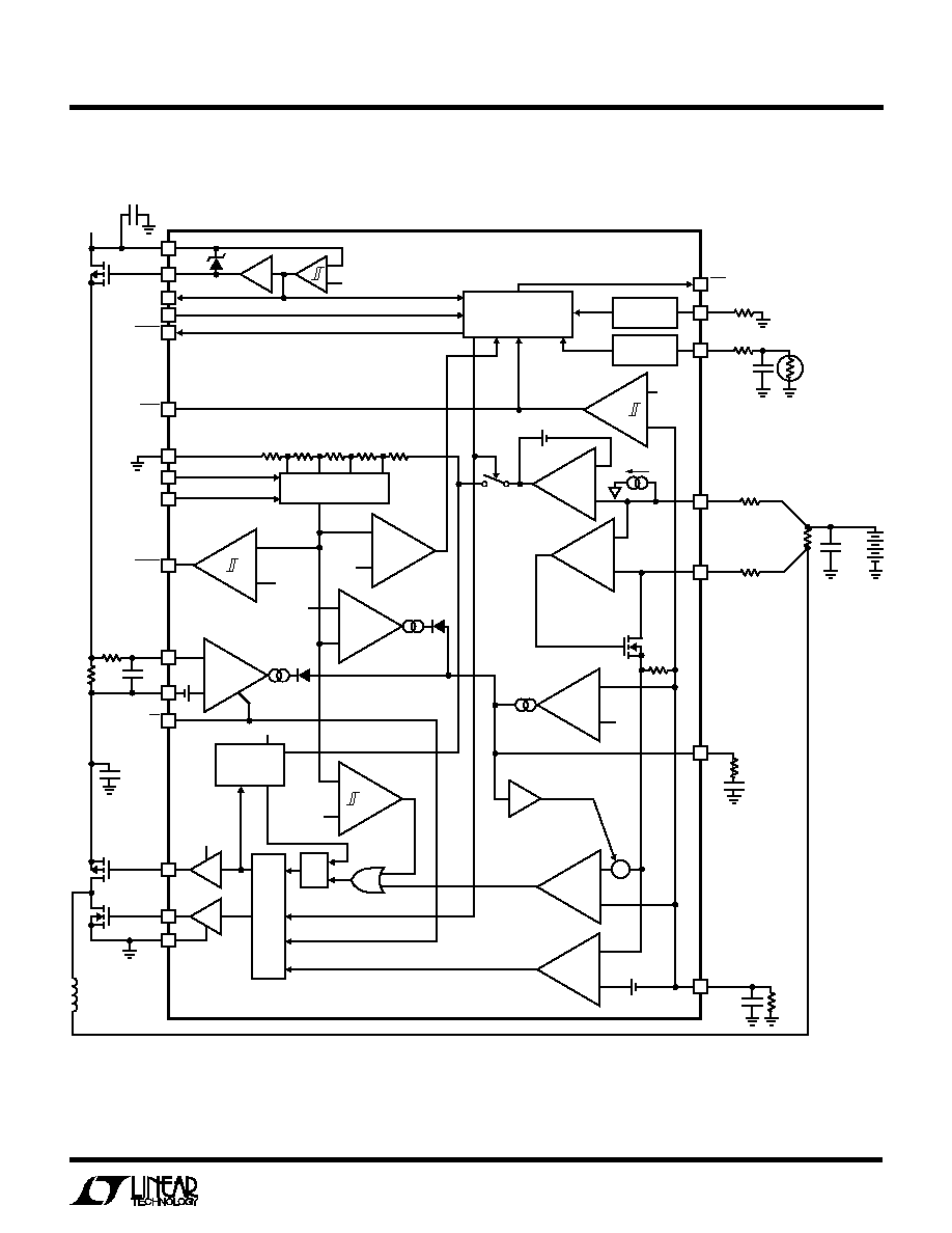
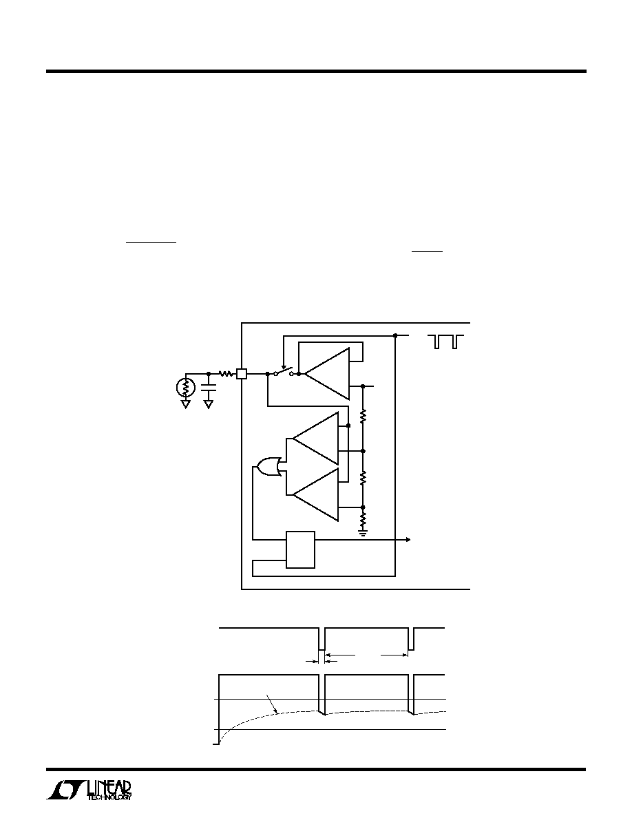
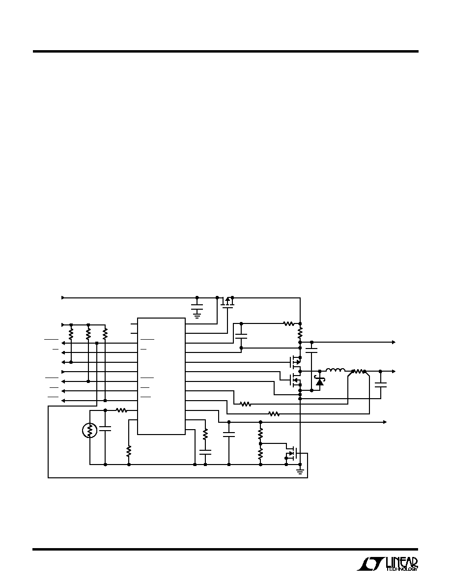
BLOCK DIAGRA
W
≠
+
≠
+
7
6
16
9k
1.19V
11.67
µ
A
TBAD
RESTART
MUX
1.105V
EA
g
m
= 1m
g
m
= 1m
g
m
= 1.4m
708mV
1.19V
3C4C
FLAG
GND
CHEM
8
LOBAT
13
20
I
CL
TGATE
BGATE
Q1
Q2
18
CLP
100mV
15nF
20
µ
F
R
CL
5k
19
CLN
22
PGND
L1
397mV
CHG
R
T
NTC
0.47
µ
F
10k
NTC
R
RT
≠
+
≠
+
CL1
TIMER/CONTROLLER
THERMISTOR
OSCILLATOR
2
4
9
BAT
3k
R
SENSE
CSP
ITH
10
32.4k
WATCHDOG
DETECT t
OFF
CLN
DCIN
OV
OSCILLATOR
1.28V
PWM
LOGIC
S
R
Q
CHARGE
I
REV
≠
+
I
CMP
+
≠
˜
5
BUFFERED ITH
21
PROG
4007 BD
R
PROG
26.7k
0.0047
µ
F
11
17
FAULT 5
SHDN 24
ACP 3
INFET
Q3
DCIN
0.1
µ
F
V
IN
23
1
≠
+
CLN
5.8V
3k
20
µ
F
6K
0.12
µ
F
15
14
≠
+
CA1
CA2
≠
+
≠
+
C/10
35mV
≠
+
≠
+
17mV
8
LTC4007
4007i
TEST CIRCUIT
≠
+
≠
+
EA
LT1055
LTC4007
V
REF
CHEM
3C4C
BAT
DIVIDER/
MUX
16
7
15
ITH
0.6V
4007 TC
10
OPERATIO
U
Overview
The LTC4007 is a synchronous current mode PWM step-
down (buck) switcher battery charger controller. The
charge current is programmed by the combination of a
program resistor (R
PROG
) from the PROG pin to ground
and a sense resistor (R
SENSE
) between the CSP and BAT
pins. The final float voltage is programmed to one of four
values (12.3V, 12.6V, 16.4V, 16.8V) with
±
1% maximum
accuracy using pins 3C4C and CHEM. Charging begins
when the potential at the DCIN pin rises above the voltage
at BAT (and the UVLO voltage) and the SHDN pin is low; the
CHG pin is set low. At the beginning of the charge cycle, if
the cell voltage is below 2.5V (2.44V if CHEM is low), the
LOBAT pin will be low. The LOBAT indicator can be used
to reduce the charging current to a low value, typically
10% of full scale. If the cell voltage stays below 2.5V for
25% of the total charge time, the charge sequence will be
terminated immediately and the FAULT pin will be set low.
An external thermistor network is sampled at regular
intervals. If the thermistor value exceeds design limits,
charging is suspended and the FAULT pin is set low. If the
thermistor value returns to an acceptable value, charging
resumes and the FAULT pin is set high. An external resistor
on the R
T
pin sets the total charge time. The timer can be
defeated by forcing the CHG pin to a low voltage.
As the battery approaches the final float voltage, the
charge current will begin to decrease. When the current
drops to 10% of the full-scale charge current, an internal
C/10 comparator will indicate this condition by latching
the FLAG pin low. The charge timer is also reset to 1/4 of
the total charge time when FLAG goes low. If this condition
is caused by an input current limit condition, described
below, then the FLAG indicator will be inhibited. When a
time-out occurs, charging is terminated immediately and
the CHG pin is forced to a high impedance state. The
charger will automatically restart if the cell voltage is
below 3.9V (or 3.81V if CHEM is low). To restart the charge
cycle manually, simply remove the input voltage and
reapply it, or set the SHDN pin high momentarily. When
the input voltage is not present, the charger goes into a
sleep mode, dropping battery current drain to 15
µ
A. This
greatly reduces the current drain on the battery and
increases the standby time. The charger is inhibited any
time the SHDN pin is high.
Input FET
The input FET circuit performs two functions. It enables
the charger if the input voltage is higher than the CLN pin
and provides the logic indicator of AC present on the ACP
pin. It controls the gate of the input FET to keep a low
forward voltage drop when charging and also prevents
reverse current flow through the input FET.
If the input voltage is less than V
CLN
, it must go at least
170mV higher than V
CLN
to activate the charger. When this
occurs the ACP pin is released and pulled up with an
external load to indicate that the adapter is present. The
9
LTC4007
4007i
gate of the input FET is driven to a voltage sufficient to keep
a low forward voltage drop from drain to source. If the
voltage between DCIN and CLN drops to less than 25mV,
the input FET is turned off slowly. If the voltage between
DCIN and CLN is ever less than ≠ 25mV, then the input FET
is turned off in less than 10
µ
s to prevent significant
reverse current from flowing in the input FET. In this
condition, the ACP pin is driven low and the charger is
disabled.
Battery Charger Controller
The LTC4007 charger controller uses a constant off-time,
current mode step-down architecture. During normal op-
eration, the top MOSFET is turned on each cycle when the
oscillator sets the SR latch and turned off when the main
current comparator I
CMP
resets the SR latch. While the top
MOSFET is off, the bottom MOSFET is turned on until
either the inductor current trips the current comparator
I
REV
or the beginning of the next cycle. The oscillator uses
the equation:
t
V
V
V
f
OFF
DCIN
BAT
DCIN
OSC
=
≠
∑
to set the bottom MOSFET on time. The result is a nearly
constant switching frequency over a wide input/output
voltage range. This activity is diagrammed in Figure 1.
TGATE
OFF
ON
BGATE
INDUCTOR
CURRENT
t
OFF
TRIP POINT SET BY ITH VOLTAGE
ON
OFF
4006 F01
Figure 1
OPERATIO
U
Table 1. Truth Table For Indicator States
TIMER
MODE
DCIN
SHDN
ACP**
LOBAT
FLAG** FAULT**
I
CL
STATE
CHG**
Shut down by low adapter voltage
<BAT
LOW
LOW
LOW
HIGH
HIGH
LOW
Reset
HIGH
Charging a low bat
>BAT
LOW
HIGH
LOW
HIGH*
HIGH*
HIGH*
Running
LOW
Normal charging
>BAT
LOW
HIGH
HIGH
HIGH
HIGH*
HIGH*
Running
LOW
Input current limited charging
>BAT
LOW
HIGH
HIGH
HIGH*
HIGH*
LOW
Running
LOW
Charger paused due to thermistor out of range
>BAT
LOW
HIGH
X
X
LOW
HIGH
Paused
LOW
(from
NTC)
Shut down by SHDN pin
X
HIGH
X
X
HIGH
HIGH
LOW
Reset
HIGH
Terminated by low-battery fault (Note 1)
>BAT
LOW
HIGH
LOW
HIGH*
LOW
LOW
>T/4
HIGH
(Faulted)
Timer is reset when FLAG goes low, then
>BAT
LOW
HIGH
HIGH
LOW
HIGH
LOW
>T/4
HIGH
terminates after 1/4 T
after
(Waiting
FLAG =
for Restart)
LOW
Terminated by expired timer
>BAT
LOW
HIGH
HIGH
HIGH
HIGH
LOW
>T
HIGH
(Waiting
for Restart
Timer defeated
X
X
X
X
X
X
X
X
Forced LOW
Shut down by undervoltage lockout
>BAT
LOW
HIGH
HIGH
HIGH
HIGH*
LOW
Reset
HIGH*
+ <UVL
*Most probable condition X = Don't care, ** Open-drain output HIGH = OPEN with pull-up
Note 1: If a depleted battery is inserted while the charger is in this state, the
charger must be reset to initiate charging.
10
LTC4007
4007i
The peak inductor current, at which I
CMP
resets the SR
latch, is controlled by the voltage on ITH. ITH is in turn
controlled by several loops, depending upon the situation
at hand. The average current control loop converts the
voltage between CSP and BAT to a representative current.
Error amp CA2 compares this current against the desired
current programmed by R
PROG
at the PROG pin and
adjusts ITH until:
V
R
V
V
A
k
k
REF
PROG
CSP
BAT
=
+
µ
≠
.
∑
11 67
3
3
therefore,
I
V
R
A
k
R
CHARGE MAX
REF
PROG
SENSE
(
)
≠
.
∑
=
µ
11 67
3
The voltage at BAT is divided down by an internal resistor
divider and is used by error amp EA to decrease ITH if the
divider voltage is above the 1.19V reference. When the
charging current begins to decrease, the voltage at PROG
will decrease in direct proportion. The voltage at PROG is
then given by:
V
I
R
A
k
R
k
PROG
CHARGE
SENSE
PROG
=
+
µ
(
)
∑
.
∑
∑
11 67
3
3
V
PROG
is plotted in Figure 2.
The amplifier CL1 monitors and limits the input current,
normally from the AC adapter to a preset level (100mV/
R
CL
). At input current limit, CL1 will decrease the ITH
OPERATIO
U
I
CHARGE
(% OF MAXIMUM CURRENT)
0
0
V
PROG
(V)
0.2
0.4
0.6
0.8
20
40
60
80
100
4007 F02
1.0
1.2
1.19V
0.309V
Figure 2. V
PROG
vs I
CHARGE
voltage, thereby reducing charging current. The I
CL
indica-
tor output will go low when this condition is detected and
the FLAG indicator will be inhibited if it is not already LOW.
If the charging current decreases below 10% to 15% of
programmed current while engaged in input current lim-
iting, BGATE will be forced low to prevent the charger from
discharging the battery. Audible noise can occur in this
mode of operation.
An overvoltage comparator guards against voltage tran-
sient overshoots (>7% of programmed value). In this
case, both MOSFETs are turned off until the overvoltage
condition is cleared. This feature is useful for batteries
which "load dump" themselves by opening their protec-
tion switch to perform functions such as calibration or
pulse mode charging.
PWM Watchdog Timer
There is a watchdog timer that observes the activity on the
BGATE and TGATE pins. If TGATE stops switching for
more than 40
µ
s, the watchdog activates and turns off the
top MOSFET for about 400ns. The watchdog engages to
prevent very low frequency operation in dropout--a po-
tential source of audible noise when using ceramic input
and output capacitors.
Charger Start-Up
When the charger is enabled, it will not begin switching
until the ITH voltage exceeds a threshold that assures
initial current will be positive. This threshold is 5% to 15%
of the maximum programmed current. After the charger
begins switching, the various loops will control the current
at a level that is higher or lower than the initial current. The
duration of this transient condition depends upon the loop
compensation, but is typically less than 100
µ
s.
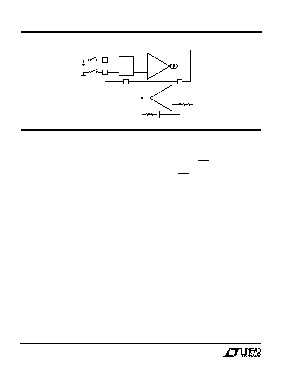
Thermistor Detection
The thermistor detection circuit is shown in Figure 3. It
requires an external resistor and capacitor in order to
function properly.
The thermistor detector performs a sample-and-hold func-
tion. An internal clock, whose frequency is determined by
11
LTC4007
4007i
OPERATIO
U
CLK
(NOT TO
SCALE)
V
NTC
t
SAMPLE
VOLTAGE ACROSS THERMISTOR
t
HOLD
4007 F04
COMPARATOR HIGH LIMIT
COMPARATOR LOW LIMIT
Figure 4
6
NTC
LTC4007
S1
R9
32.4k
C7
0.47
µ
F
R
TH
10k
NTC
≠
+
≠
+
≠
+
60k
~4.5V
CLK
45k
15k
TBAD
4007 F03
D
C
Q
Figure 3
the timing resistor connected to R
T
, keeps switch S1
closed to sample the thermistor:
t
SAMPLE
= 127.5 ∑ 20 ∑ R
RT
∑ 17.5pF = 16.2ms,
for R
RT
= 309k
The external RC network is driven to approximately 4.5V
and settles to a final value across the thermistor of:
V
V R
R
R
RTH FINAL
TH
TH
(
)
.
∑
=
+
4 5
9
This voltage is stored by C7. Then the switch is opened for
a short period of time to read the voltage across the
thermistor.
t
HOLD
= 10 ∑ R
RT
∑ 17.5pF = 64
µ
s,
for R
RT
= 309k
When the t
HOLD
interval ends the result of the thermistor
testing is stored in the D flip-flop (DFF). If the voltage at
NTC is within the limits provided by the resistor divider
feeding the comparators, then the NOR gate output will be
low and the DFF will set T
BAD
to zero and charging will
continue. If the voltage at NTC is outside of the resistor
divider limits, then the DFF will set T
BAD
to one, the charger
will be shut down, FAULT pin is set low and the timer will
be suspended until T
BAD
returns to zero (see Figure 4).
12
LTC4007
4007i
APPLICATIO S I FOR ATIO
W
U
U
U
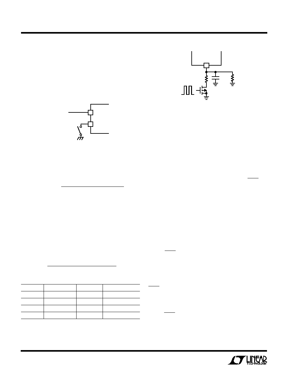
Battery Detection
It is generally not good practice to connect a battery while
the charger is running. The timer is in an unknown state
and the charger could provide a large surge current into
the battery for a brief time. The Figure 5 circuit keeps the
charger shut down and the timer reset while a battery is not
connected.
increased to reduce the ripple caused by the R
PROG
switching. The compensation capacitor at ITH will prob-
ably need to be increased also to improve stability and
prevent large overshoot currents during start-up condi-
tions. Charging current will be proportional to the duty
cycle of the switch with full current at 100% duty cycle and
zero current when Q1 is off.
Maintaining C/10 Accuracy
The C/10 comparator threshold that drives the FLAG pin
has a fixed threshold of approximately V
PROG
= 400mV.
This threshold works well when R
PROG
is 26.7k, but will
not yield a 10% charging current indication if R
PROG
is a
different value. There are situations where a standard
value of R
SENSE
will not allow the desired value of charging
current when using the preferred R
PROG
value. In these
cases, where the full-scale voltage across R
SENSE
is within
±
20mV of the 100mV full-scale target, the input resistors
connected to CSP and BAT can be adjusted to provide the
desired maximum programming current as well as the
correct FLAG trip point.
For example, the desired max charging current is 2.5A but
the best R
SENSE
value is 0.033
. In this case, the voltage
across R
SENSE
at maximum charging current is only
82.5mV, normally R
PROG
would be 30.1k but the nominal
FLAG trip point is only 5% of maximum charging current.
If the input resistors are reduced by the same amount as
the full-scale voltage is reduced then, R4 = R5 = 2.49k and
R
PROG
= 26.7k, the maximum charging current is still 2.5A
but the FLAG trip point is maintained at 10% of full scale.
There are other effects to consider. The voltage across the
current comparator is scaled to obtain the same values as
the 100mV sense voltage target, but the input referred
1 DCIN
LTC4007
ADAPTER
POWER
SWITCH CLOSED
WHEN BATTERY
CONNECTED
24 SHDN
4007 F05
Figure 5
Charger Current Programming
The basic formula for charging current is:
I
V
k
R
V
R
CHARGE MAX
REF
PROG
SENSE
(
)
∑
/
≠ .
=
3
0 035
V
REF
= 1.19V
This leaves two degrees of freedom: R
SENSE
and R
PROG
.
The 3k input resistors must not be altered since internal
currents and voltages are trimmed for this value. Pick
R
SENSE
by setting the average voltage between C
SP
and
BAT to be close to 100mV during maximum charger
current. Then R
PROG
can be determined by solving the
above equation for R
PROG
.
R
V
k
R
I
V
PROG
REF
SENSE
CHARGE MAX
=
+
∑
∑
.
(
)
3
0 035
Table 2. Recommended R
SNS
and R
PROG
Resistor Values
I
MAX
(A)
R
SENSE
(
) 1%
R
SENSE
(W)
R
PROG
(k
) 1%
1.0
0.100
0.25
26.7
2.0
0.050
0.25
26.7
3.0
0.033
0.5
26.7
4.0
0.025
0.5
26.7
Charging current can be programmed by pulse width
modulating R
PROG
with a switch Q1 to R
PROG
at a fre-
quency higher than a few kHz (Figure 6). C
PROG
must be
Figure 6. PWM Current Programming
R
Z
102k
C
PROG
4007 F06
PROG
11
LTC4007
Q1
2N7002
R
PROG
0V
5V
13
LTC4007
4007i
sense voltage is reduced, causing some careful consider-
ation of the ripple current. Input referred maximum com-
parator threshold is 117mV, which is the same ratio of 1.4x
the DC target. Input referred I
REV
threshold is scaled back
to ≠24mV. The current at which the switcher starts will be
reduced as well so there is some risk of boost activity.
These concerns can be addressed by using a slightly larger
inductor to compensate for the reduction of tolerance to
ripple current.
Charger Voltage Programming
Pins CHEM and C3C4 are used to program the charger final
output voltage. The CHEM pin programs Li-Ion battery
chemistry for 4.1V/cell (low) or 4.2V/cell (high). The C3C4
pin selects either 3 series cells (low) or 4 series cells
(high). It is recommended that these pins be shorted to
ground (logic low) or left open (logic high) to effect the
desired logic level. Use open-collector or open-drain out-
puts when interfacing to the CHEM and 3C4C pins from a
logic control circuit.
Table 3. Charger Voltage Programming
V
FINAL
(V)
3C4C
CHEM
12.3
LOW
LOW
12.6
LOW
HIGH
16.4
HIGH
LOW
16.8
HIGH
HIGH
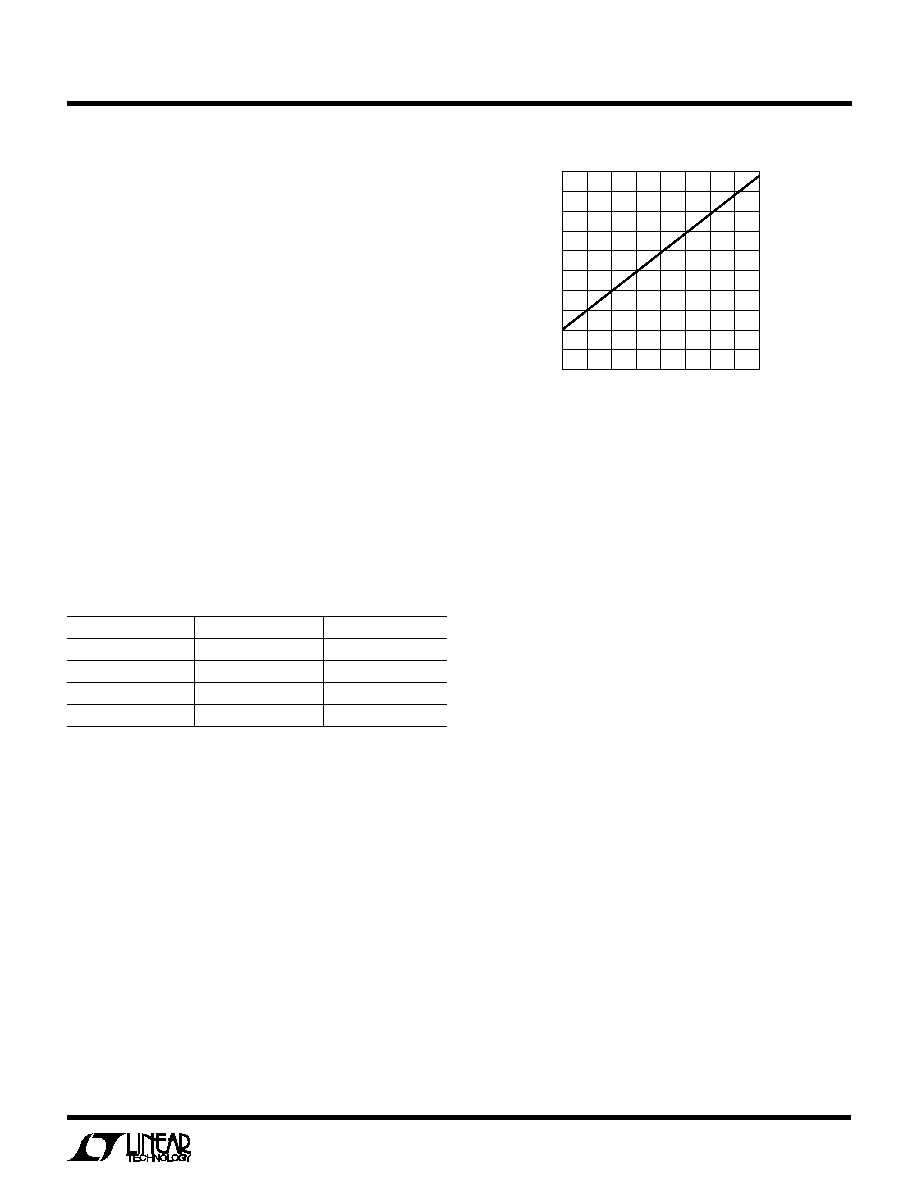
Setting the Timer Resistor
The charger termination timer is designed for a range of
1hour to 3 hour with a
±
15% uncertainty. The timer is
programmed by the resistor R
RT
using the following
equation:
t
TIMER
= 2
27
∑ R
RT
∑ 175pF
It is important to keep the parasitic capacitance on the R
T
pin to a minimum. The trace connecting R
T
to R
RT
should
be as short as possible.
Soft-Start
The LTC4007 is soft started by the 0.12
µ
F capacitor on the
ITH pin. On start-up, ITH pin voltage will rise quickly to
0.5V, then ramp up at a rate set by the internal 40
µ
A pull-
up current and the external capacitor. Battery charging
APPLICATIO S I FOR ATIO
W
U
U
U
current starts ramping up when ITH voltage reaches 0.8V
and full current is achieved with ITH at 2V. With a 0.12
µ
F
capacitor, time to reach full charge current is about 2ms
and it is assumed that input voltage to the charger will
reach full value in less than 2ms. The capacitor can be
increased up to 1
µ
F if longer input start-up times are
needed.
Input and Output Capacitors
The input capacitor (C2) is assumed to absorb all input
switching ripple current in the converter, so it must have
adequate ripple current rating. Worst-case RMS ripple
current will be equal to one half of output charging current.
Actual capacitance value is not critical. Solid tantalum low
ESR capacitors have high ripple current rating in a rela-
tively small surface mount package,
but caution must be
used when tantalum capacitors are used for input or
output bypass. High input surge currents can be created
when the adapter is hot-plugged to the charger or when a
battery is connected to the charger. Solid tantalum capaci-
tors have a known failure mechanism when subjected to
very high turn-on surge currents. Only Kemet T495 series
of "Surge Robust" low ESR tantalums are rated for high
surge conditions such as battery to ground.
The relatively high ESR of an aluminum electrolytic for C1,
located at the AC adapter input terminal, is helpful in
reducing ringing during the hot-plug event. Refer to AN88
for more information.
Figure 7. t
TIMER
vs R
RT
R
RT
(k
)
100
0
t
TIMER
(MINUTES)
20
60
80
100
200
140
200
300
350
4007 F07
40
160
180
120
150
250
400 450
500
14
LTC4007
4007i
Highest possible voltage rating on the capacitor will mini-
mize problems. Consult with the manufacturer before use.
Alternatives include new high capacity ceramic (at least
20
µ
F) from Tokin, United Chemi-Con/Marcon, et al. Other
alternative capacitors include OS-CON capacitors from
Sanyo.
The output capacitor (C3) is also assumed to absorb
output switching current ripple. The general formula for
capacitor current is:
I
V
V
V
L f
RMS
BAT
BAT
DCIN
=
(
)
( )( )
0 29
1
1
.
≠
For example:
V
DCIN
= 19V, V
BAT
= 12.6V, L1 = 10
µ
H, and
f = 300kHz, I
RMS
= 0.41A.
EMI considerations usually make it desirable to minimize
ripple current in the battery leads, and beads or inductors
may be added to increase battery impedance at the 300kHz
switching frequency. Switching ripple current splits be-
tween the battery and the output capacitor depending on
the ESR of the output capacitor and the battery imped-
ance. If the ESR of C3
is 0.2
and the battery impedance
is raised to 4
with a bead or inductor, only 5% of the
current ripple will flow in the battery.
Inductor Selection
Higher operating frequencies allow the use of smaller
inductor and capacitor values. A higher frequency gener-
ally results in lower efficiency because of MOSFET gate
charge losses. In addition, the effect of inductor value on
ripple current and low current operation must also be
considered. The inductor ripple current
I
L
decreases
with higher frequency and increases with higher V
IN
.
=
( )( )
I
f L
V
V
V
L
OUT
OUT
IN
1
1≠
Accepting larger values of
I
L
allows the use of low
inductances, but results in higher output voltage ripple
and greater core losses. A reasonable starting point for
setting ripple current is
I
L
= 0.4(I
MAX
). In no case should
I
L
exceed 0.6(I
MAX
) due to limits imposed by I
REV
and
CA1. Remember the maximum
I
L
occurs at the maxi-
mum input voltage. In practice 10
µ
H is the lowest value
recommended for use.
Lower charger currents generally call for larger inductor
values. Use Table 4 as a guide for selecting the correct
inductor value for your application.
Table 4
MAX AVERAGE
MINIMUM INDUCTOR
CURRENT (A)
INPUT VOLTAGE (V)
VALUE (
µ
H)
1
20
40
±
20%
1
>20
56
±
20%
2
20
20
±
20%
2
>20
30
±
20%
3
20
15
±
20%
3
>20
20
±
20%
4
20
10
±
20%
4
>20
15
±
20%
Charger Switching Power MOSFET
and Diode Selection
Two external power MOSFETs must be selected for use
with the charger: a P-channel MOSFET for the top (main)
switch and an N-channel MOSFET for the bottom (syn-
chronous) switch.
The peak-to-peak gate drive levels are set internally. This
voltage is typically 6V. Consequently, logic-level threshold
MOSFETs must be used. Pay close attention to the BV
DSS
specification for the MOSFETs as well; many of the logic
level MOSFETs are limited to 30V or less.
Selection criteria for the power MOSFETs include the "ON"
resistance R
DS(ON)
, total gate capacitance QG, reverse
transfer capacitance C
RSS
, input voltage and maximum
output current. The charger is operating in continuous
mode at moderate to high currents so the duty cycles for
the top and bottom MOSFETs are given by:
Main Switch Duty Cycle = V
OUT
/V
IN
Synchronous Switch Duty Cycle = (V
IN
≠ V
OUT
)/V
IN
.
APPLICATIO S I FOR ATIO
W
U
U
U
15
LTC4007
4007i
The MOSFET power dissipations at maximum output
current are given by:
PMAIN = V
OUT
/V
IN
(I
MAX
)
2
(1 +
T)R
DS(ON)
+ k(V
IN
)
2
(I
MAX
)(C
RSS
)(f
OSC
)
PSYNC = (V
IN
≠ V
OUT
)/V
IN
(I
MAX
)
2
(1 +
T)R
DS(ON)
Where
T is the temperature dependency of R
DS(ON)
and
k is a constant inversely related to the gate drive current.
Both MOSFETs have I
2
R losses while the PMAIN equation
includes an additional term for transition losses, which are
highest at high input voltages. For V
IN
< 20V the high
current efficiency generally improves with larger MOSFETs,
while for V
IN
> 20V the transition losses rapidly increase
to the point that the use of a higher R
DS(ON)
device with
lower C
RSS
actually provides higher efficiency. The syn-
chronous MOSFET losses are greatest at high input volt-
age or during a short circuit when the duty cycle in this
switch in nearly 100%. The term (1 +
T) is generally
given for a MOSFET in the form of a normalized R
DS(ON)
vs
temperature curve, but
= 0.005/
∞
C can be used as an
approximation for low voltage MOSFETs. C
RSS
= Q
GD
/
V
DS
is usually specified in the MOSFET characteristics. The
constant k = 2 can be used to estimate the contributions of
the two terms in the main switch dissipation equation.
If the charger is to operate in low dropout mode or with a
high duty cycle greater than 85%, then the topside
P-channel efficiency generally improves with a larger
MOSFET. Using asymmetrical MOSFETs may achieve cost
savings or efficiency gains.
The Schottky diode D1, shown in the Typical Application
on the back page, conducts during the dead-time between
the conduction of the two power MOSFETs. This prevents
the body diode of the bottom MOSFET from turning on and
storing charge during the dead-time, which could cost as
much as 1% in efficiency. A 1A Schottky is generally a
good size for 4A regulators due to the relatively small
average current. Larger diodes can result in additional
transition losses due to their larger junction capacitance.
The diode may be omitted if the efficiency loss can be
tolerated.
APPLICATIO S I FOR ATIO
W
U
U
U
Figure 8. Adapter Current Limiting
Calculating IC Power Dissipation
The power dissipation of the LTC4007 is dependent upon
the gate charge of the top and bottom MOSFETs (QG1 &
QG2 respectively) The gate charge is determined from the
manufacturer's data sheet and is dependent upon both the
gate voltage swing and the drain voltage swing of the
MOSFET. Use 6V for the gate voltage swing and V
DCIN
for
the drain voltage swing.
PD = V
DCIN
∑ (f
OSC
(QG1 + QG2) + I
Q
)
Example:
V
DCIN
= 19V, f
OSC
= 345kHz, QG1 = QG2 = 15nC.
PD = 235mW
Adapter Limiting
An important feature of the LTC4007 is the ability to
automatically adjust charging current to a level which
avoids overloading the wall adapter. This allows the prod-
uct to operate at the same time that batteries are being
charged without complex load management algorithms.
Additionally, batteries will automatically be charged at the
maximum possible rate of which the adapter is capable.
This feature is created by sensing total adapter output
current and adjusting charging current downward if a
preset adapter current limit is exceeded. True analog
control is used, with closed-loop feedback ensuring that
adapter load current remains within limits. Amplifier CL1
in Figure 8 senses the voltage across R
CL
, connected
100mV
≠
+
5k
CLP
LTC4007
18
CLN
19
4007 F08
15nF
+
R
CL
*
C
IN
V
IN
CL1
AC ADAPTER
INPUT
*R
CL
=
100mV
ADAPTER CURRENT LIMIT
+
16
LTC4007
4007i
between the CLP and CLN pins. When this voltage exceeds
100mV, the amplifier will override programmed charging
current to limit adapter current to 100mV/R
CL
. A lowpass
filter formed by 5k
and 15nF is required to eliminate
switching noise. If the current limit is not used, CLP should
be connected to DCIN.
Note that the I
CL
pin will be asserted when the voltage
across R
CL
is 93mV, before the adapter limit regulation
threshold.
Setting Input Current Limit
To set the input current limit, you need to know the
minimum wall adapter current rating. Subtract 5% for the
input current limit tolerance and use that current to deter-
mine the resistor value.
R
CL
= 100mV/I
LIM
I
LIM
= Adapter Min Current ≠
(Adapter Min Current ∑ 5%)
Table 5. Common R
CL
Resistor Values
ADAPTER
RCL VALUE*
RCL POWER
RCL POWER
RATING (A)
(
) 1%
DISSIPATION (W)
RATING (W)
1.5
0.06
0.135
0.25
1.8
0.05
0.162
0.25
2
0.045
0.18
0.25
2.3
0.039
0.206
0.25
2.5
0.036
0.225
0.5
2.7
0.033
0.241
0.5
3
0.03
0.27
0.5
* Values shown above are rounded to nearest standard value.
As is often the case, the wall adapter will usually have at
least a +10% current limit margin and many times one can
simply set the adapter current limit value to the actual
adapter rating (see Table 5).
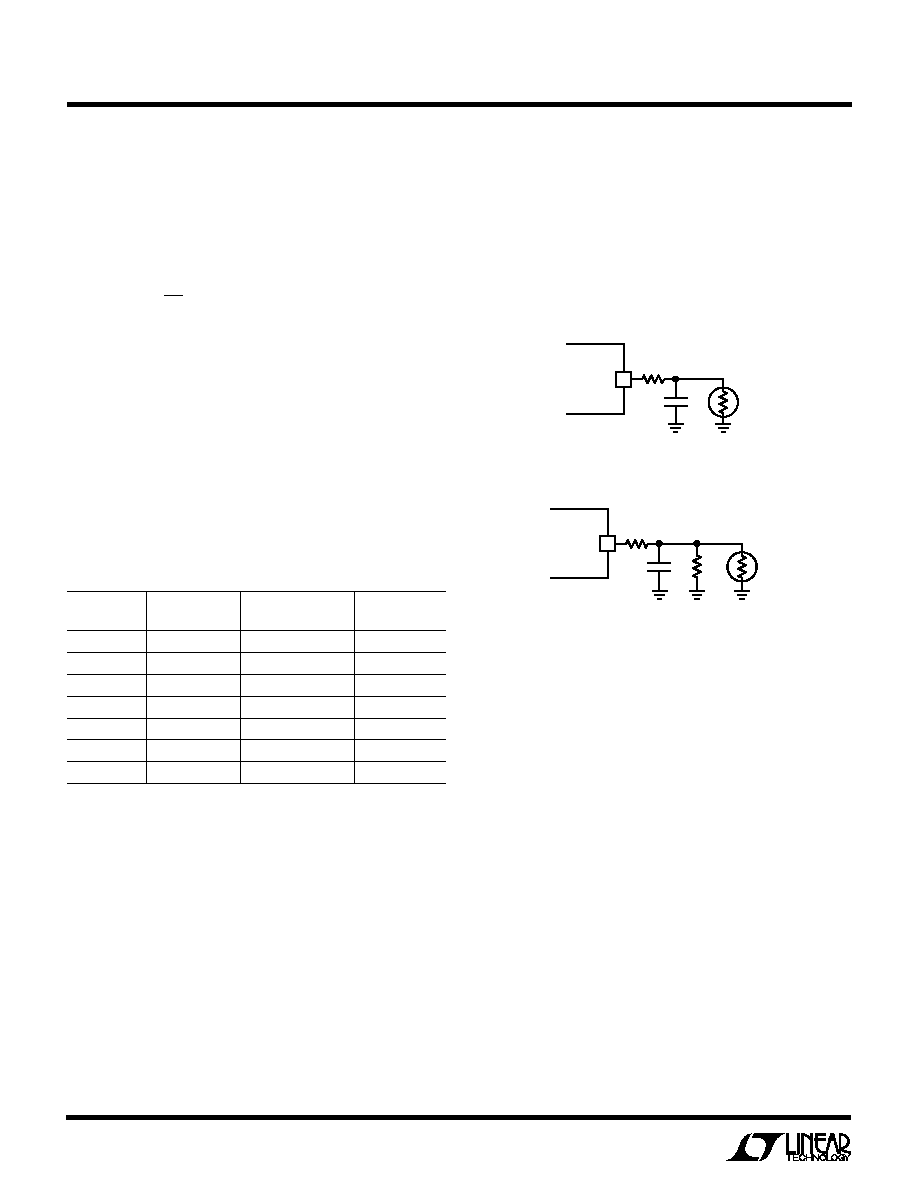
Designing the Thermistor Network
There are several networks that will yield the desired
function of voltage vs temperature needed for proper
operation of the thermistor. The simplest of these is the
voltage divider shown in Figure 9. Unfortunately, since the
HIGH/LOW comparator thresholds are fixed internally,
there is only one thermistor type that can be used in this
APPLICATIO S I FOR ATIO
W
U
U
U
network; the thermistor must have a HIGH/LOW resis-
tance ratio of 1:7. If this happy circumstance is true for
you, then simply set R9 = R
TH(LOW)
If you are using a thermistor that doesn't have a 1:7 HIGH/
LOW ratio, or you wish to set the HIGH/LOW limits to
different temperatures, then the more generic network in
Figure 10 should work.
Figure 9. Voltage Divider Thermistor Network
Figure 10. General Thermistor Network
LTC4007
NTC
R9
9
C7
R
TH
4007 F09
LTC4007
NTC
R9
9
C7
R9A
R
TH
4007 F10
Once the thermistor, R
TH
, has been selected and the
thermistor value is known at the temperature limits, then
resistors R9 and R9A are given by:
For NTC thermistors:
R9 = 6 R
TH(LOW)
∑ R
TH(HIGH)
/(R
TH(LOW)
≠ R
TH(HIGH)
)
R9A = 6 R
TH(LOW)
∑ R
TH(HIGH)
/(R
TH(LOW)
≠ 7 ∑ R
TH(HIGH)
)
For PTC thermistors:
R9 = 6 R
TH(LOW)
∑ R
TH(HIGH)
/(R
TH(HIGH)
≠ R
TH(LOW)
)
R9A = 6 R
TH(LOW)
∑ R
TH(HIGH)
/(R
TH(HIGH)
≠ 7 ∑
R
TH(LOW)
)
Example #1: 10k
NTC with custom limits
TLOW = 0
∞
C, THIGH = 50
∞
C
R
TH
= 10k at 25
∞
C,
R
TH(LOW)
= 32.582k at 0
∞
C
R
TH(HIGH)
= 3.635k at 50
∞
C
R9 = 24.55k
24.3k (nearest 1% value)
R9A = 99.6k
100k (nearest 1% value)

17
LTC4007
4007i
APPLICATIO S I FOR ATIO
W
U
U
U
Example #2: 100k
NTC
TLOW = 5
∞
C, THIGH = 50
∞
C
R
TH
= 100k at 25
∞
C,
R
TH(LOW)
= 272.05k at 5
∞
C
R
TH(HIGH)
= 33.195k at 50
∞
C
R9 = 226.9k
226k (nearest 1% value)
R9A = 1.365M
1.37M (nearest 1% value)
Example #3: 22k
PTC
TLOW = 0
∞
C, THIGH = 50
∞
C
R
TH
= 22k at 25
∞
C,
R
TH(LOW)
= 6.53k at 0
∞
C
R
TH(HIGH)
= 61.4k at 50
∞
C
R9 = 43.9k
44.2k (nearest 1% value)
R9A = 154k
Sizing the Thermistor Hold Capacitor
During the hold interval, C7 must hold the voltage across
the thermistor relatively constant to avoid false readings.
A reasonable amount of ripple on NTC during the hold
interval is about 10mV to 15mV. Therefore, the value of C7
is given by:
C7 = t
HOLD
/(R9/7 ∑ ≠ln(1 ≠ 8 ∑ 15mV/4.5V))
= 10 ∑ R
RT
∑ 17.5pF/(R9/7 ∑ ≠ ln(1 ≠ 8 ∑ 15mV/4.5V)
Example:
R9 = 24.3k
R
RT
= 309k (~2 hour timer)
C7 = 0.51
µ
F
0.56
µ
F (nearest value)
Disabling the Thermistor Function
If the thermistor is not needed, connecting a resistor
between DCIN and NTC will disable it. The resistor should
be sized to provide at least 10
µ
A with the minimum voltage
applied to DCIN and 10V at NTC. Generally, a 301k resistor
will work for DCIN less than 15V. A 499k resistor is
recommended for DCIN greater than 15V.
Conditioning Depleted Batteries
Severely depleted batteries, with less than 2.5V/cell, should
be conditioned with a trickle charge to prevent possible
damage. This trickle charge is typically 10% of the 1C rate
of the battery. The LTC4007 can automatically trickle
charge depleted batteries using the circuit in Figure 11. If
the battery voltage is less than 2.5V/cell (2.44V/cell if
CHEM is low) then the LOBAT indicator will be low and Q4
is off. This programs the charging current with R
PROG
= R6
+ R14. Charging current is approximately 300mA. When
the cell voltage becomes greater than 2.5V the LOBAT
indicator goes high, Q4 shorts out R13, then R
PROG
= R6.
Charging current is then equal to 3A.
PCB Layout Considerations
For maximum efficiency, the switch node rise and fall
times should be minimized. To prevent magnetic and
electrical field radiation and high frequency resonant prob-
lems, proper layout of the components connected to the IC
is essential. (See Figure 12.) Here is a PCB layout priority
list for proper layout. Layout the PCB using this specific
order.
1. Input capacitors need to be placed as close as possible
to switching FET's supply and ground connections.
Shortest copper trace connections possible. These
parts must be on the same layer of copper. Vias must
not be used to make this connection.
2. The control IC needs to be close to the switching FET's
gate terminals. Keep the gate drive signals short for a
clean FET drive. This includes IC supply pins that con-
nect to the switching FET source pins. The IC can be
placed on the opposite side of the PCB relative to above.
3. Place inductor input as close as possible to switching
FET's output connection. Minimize the surface area of
this trace. Make the trace width the minimum amount
needed to support current--no copper fills or pours.
Avoid running the connection using multiple layers in
parallel. Minimize capacitance from this node to any
other trace or plane.
4. Place the output current sense resistor right next to
the inductor output but oriented such that the IC's
current sense feedback traces going to resistor are not
long. The feedback traces need to be routed together
as a single pair on the same layer at any given time with
smallest trace spacing possible. Locate any filter
component on these traces next to the IC and not at the
sense resistor location.
18
LTC4007
4007i
Figure 11. Circuit Application (16.8V/3A) to Automatically Trickle Charge Depleted Batteries
3C4C
CHEM
LOBAT
I
CL
ACP
SHDN
FAULT
CHG
FLAG
NTC
R
T
LOBAT
I
CL
ACP
SHDN
FAULT
CHG
FLAG
DCIN
INFET
CLP
CLN
TGATE
BGATE
PGND
CSP
BAT
PROG
ITH
GND
LTC4007
R9 32.4k 1%
R
T
309k
1%
C7
0.47
µ
F
THERMISTOR
TIMING RESISTOR
(~2 HOURS)
R12
100k
R11
100k
R10
100k
V
LOGIC
*
*
DCIN
0V TO 20V
3A
C1
0.1
µ
F
Q3
INPUT SWITCH
C4
15nF
Q1
Q2
D1
C2
20
µ
F
L1
15
µ
H 3A
R1
4.9k
1%
R4
3.01k
1%
R5 3.01k 1%
R
SENSE
0.033
1%
R
CL
0.033
1%
C3
20
µ
F
*PIN OPEN
D1: MBRM140T3
Q1: Si4431ADY
Q2: FDC645N
Q4: 2N7002 OR BSS138
BAT
MONITOR
(CHARGING
CURRENT
MONITOR)
SYSTEM
LOAD
C6
0.12
µ
F
R7
6.04k
1%
R14
73.2k
1%
C5
0.0047
µ
F
4007 F11
R6
26.7k
1%
Q4
5. Place output capacitors next to the sense resistor
output and ground.
6. Output capacitor ground connections need to feed
into same copper that connects to the input capacitor
ground before tying back into system ground.
General Rules
7. Connection of switching ground to system ground or
internal ground plane should be single point. If the
system has an internal system ground plane, a good
way to do this is to cluster vias into a single star point
to make the connection.
8. Route analog ground as a trace tied back to IC ground
(analog ground pin if present) before connecting to
any other ground. Avoid using the system ground
plane. CAD trick: make analog ground a separate
ground net and use a 0
resistor to tie analog ground
to system ground.
9. A good rule of thumb for via count for a given high
current path is to use 0.5A per via. Be consistent.
10. If possible, place all the parts listed above on the same
PCB layer.
11. Copper fills or pours are good for all power connec-
tions except as noted above in Rule 3. You can also use
copper planes on multiple layers in parallel too--this
helps with thermal management and lower trace in-
ductance improving EMI performance further.
12. For best current programming accuracy provide a
Kelvin connection from R
SENSE
to CSP and BAT. See
Figure 12 as an example.
It is important to keep the parasitic capacitance on the R
T
,
CSP and BAT pins to a minimum. The traces connecting
these pins to their respective resistors should be as short
as possible.
APPLICATIO S I FOR ATIO
W
U
U
U
19
LTC4007
4007i
PACKAGE DESCRIPTIO
N
U
Figure 12. High Speed Switching Path
Figure 13. Kelvin Sensing of Charging Current
4007 F12
V
BAT
L1
V
IN
HIGH
FREQUENCY
CIRCULATING
PATH
BAT
SWITCH NODE
C2
C3
D1
CSP
4007 F13
DIRECTION OF CHARGING CURRENT
R
SENSE
BAT
APPLICATIO S I FOR ATIO
W
U
U
U
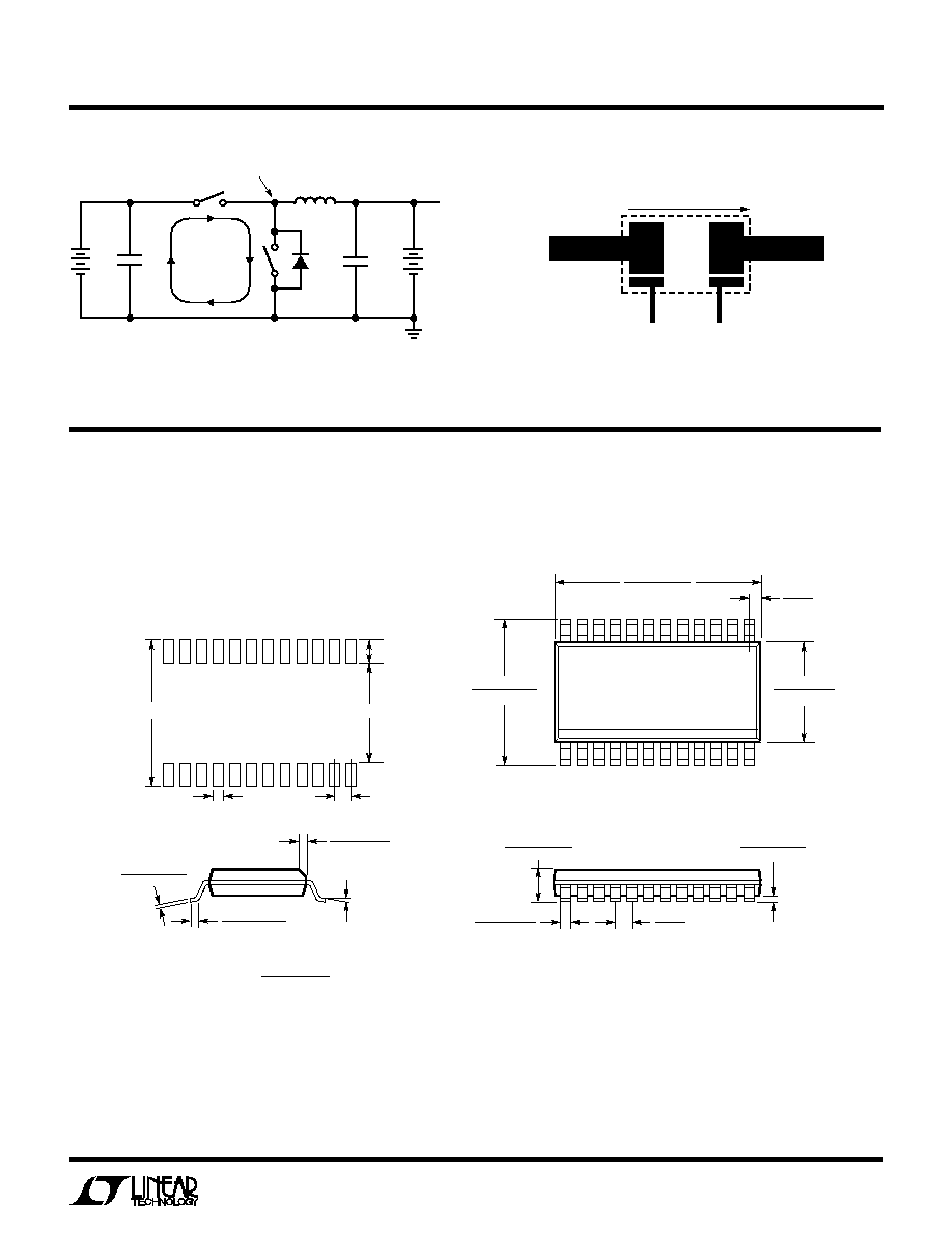
GN Package
24-Lead Plastic SSOP (Narrow .150 Inch)
(Reference LTC DWG # 05-08-1641)
.337 ≠ .344*
(8.560 ≠ 8.738)
GN24 (SSOP) 0502
1
2
3
4
5
6
7
8
9 10 11 12
.229 ≠ .244
(5.817 ≠ 6.198)
.150 ≠ .157**
(3.810 ≠ 3.988)
16
17
18
19
20
21
22
23
24
15 1413
.016 ≠ .050
(0.406 ≠ 1.270)
.015
±
.004
(0.38
±
0.10)
◊
45
∞
0
∞
≠ 8
∞
TYP
.007 ≠ .0098
(0.178 ≠ 0.249)
.053 ≠ .068
(1.351 ≠ 1.727)
.008 ≠ .012
(0.203 ≠ 0.305)
.004 ≠ .0098
(0.102 ≠ 0.249)
.0250
(0.635)
BSC
.033
(0.838)
REF
.254 MIN
RECOMMENDED SOLDER PAD LAYOUT
.150 ≠ .165
.0250 TYP
.0165
±
.0015
.045
±
.005
*DIMENSION DOES NOT INCLUDE MOLD FLASH. MOLD FLASH
SHALL NOT EXCEED 0.006" (0.152mm) PER SIDE
**DIMENSION DOES NOT INCLUDE INTERLEAD FLASH. INTERLEAD
FLASH SHALL NOT EXCEED 0.010" (0.254mm) PER SIDE
INCHES
(MILLIMETERS)
NOTE:
1. CONTROLLING DIMENSION: INCHES
2. DIMENSIONS ARE IN
3. DRAWING NOT TO SCALE
20
LTC4007
4007i
Linear Technology Corporation
1630 McCarthy Blvd., Milpitas, CA 95035-7417
(408) 432-1900
q
FAX: (408) 434-0507
q
www.linear.com
©
LINEAR TECHNOLOGY CORPORATION 2003
LT/TP 0103 1.5K ∑ PRINTED IN USA
RELATED PARTS
PART NUMBER
DESCRIPTION
COMMENTS
LT
Æ
1511
Constant-Current/Constant-Voltage 3A Battery
High Efficiency Current Mode PWM with 4A Internal Switch
Charger with Input Current Limiting
LT1513
SEPIC Constant- or Programmable-Current/
Charger Input Voltage May Be Higher, Equal to or Lower Than Battery Voltage;
Constant-Voltage Battery Charger
Charges Any Number of Cells Up to 20V, 500kHz Switching Frequency
LT1571
1.5A Switching Charger
1- or 2-Cell Li-Ion, 500kHz or 200kHz Switching Frequency, Termination Flag
LTC1628-PG
2-Phase, Dual Synchronous Step-Down Controller
Minimizes C
IN
and C
OUT
, Power Good Output, 3.5V
V
IN
36V
LTC1709
2-Phase, Dual Synchronous Step-Down Controller
Up to 42A Output, Minimum C
IN
and C
OUT
, Uses Smallest Components for
with VID
Intel and AMD Processors
LTC1729
LT1769
2A Switching Battery Charger
Constant-Current/Constant-Voltage Switching Regulator, Input Current
Limiting Maximizes Charge Current
LTC1778
Wide Operating Range, No R
SENSE
Synchronous
2% to 90% Duty Cycle at 200kHz, Stable with Ceramic C
OUT
Step-Down Controller
LTC1960
Dual Battery Charger/Selector with SPI Interface
Simultaneous Charge or Discharge of Two Batteries, DAC Programmable
Current and Voltage, Input Current Limiting Maximizes Charge Current
LTC3711
No R
SENSE
TM
Synchronous Step-Down Controller
3.5V
V
IN
36V, 0.925V
V
OUT
2V, for Transmeta, AMD and Intel
with VID
Mobile Processors
LTC4006
Small, High Efficiency, Fixed Voltage,
Constant-Current/Constant-Voltage Switching Regulator with Termination
Lithium-Ion Battery Charger
Timer, AC Adapter Current Limit and Thermistor Sensor in a Small
16-Pin Package
LTC4008
High Efficiency, Programmable Voltage/Current
Constant-Current/Constant-Voltage Switching Regulator, Resistor Voltage/
Battery Charger
Current Programming, AC Adapter Current Limit and Thermistor Sensor
No R
SENSE
is a trademark of Linear Technology Corporation.
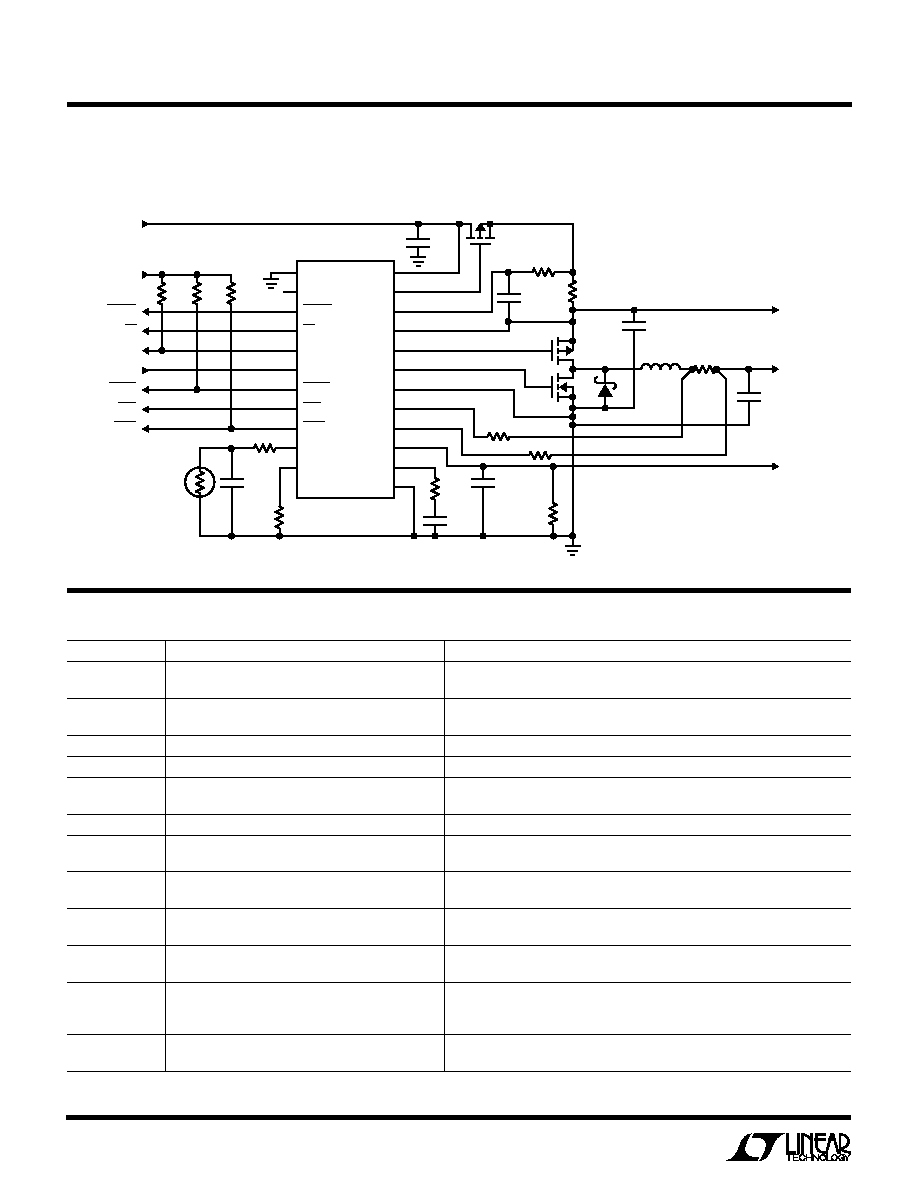
12.6V, 4A Li-Ion Battery Charger
3C4C
CHEM
LOBAT
I
CL
ACP
SHDN
FAULT
CHG
FLAG
NTC
R
T
LOBAT
I
CL
ACP
SHDN
FAULT
CHG
FLAG
DCIN
INFET
CLP
CLN
TGATE
BGATE
PGND
CSP
BAT
PROG
ITH
GND
LTC4007
R9 32.4k 1%
R
RT
309k
1%
C7
0.47
µ
F
THERMISTOR
10k
NTC
TIMING RESISTOR
(~2 HOURS)
R12
100k
*
R11
100k
R10
100k
V
LOGIC
DCIN
0V TO 20V
3A
C1
0.1
µ
F
Q3
INPUT SWITCH
C4
15nF
Q1
Q2
D1
C2
20
µ
F
L1
10
µ
H 4A
R1
4.9k
1%
R4
3.01k 1%
R5 3.01k 1%
R
SENSE
0.025
1%
R
CL
0.033
1%
C3
20
µ
F
BAT
CHARGING
CURRENT
MONITOR
SYSTEM
LOAD
C6
0.12
µ
F
R7
6.04k
1%
R
PROG
26.7k
1%
C5
0.0047
µ
F
*PIN OPEN
D1: MBRS130T3
Q1: Si4431ADY
Q2: FDC645N
4007 TA02
TYPICAL APPLICATIO
U