 | ÐлекÑÑоннÑй компоненÑ: LTC4253 | СкаÑаÑÑ:  PDF PDF  ZIP ZIP |
Äîêóìåíòàöèÿ è îïèñàíèÿ www.docs.chipfind.ru
LTC4253
1
4253f
The LTC
®
4253 negative voltage Hot Swap
TM
controller
allows a board to be safely inserted and removed from a
live backplane. Output current is controlled by three stages
of current-limiting: a timed circuit breaker, active current
limiting and a fast feedforward path that limits peak
current under worst-case catastrophic fault conditions.
The LTC4253 latches off after a circuit fault.
Programmable undervoltage and overvoltage detectors
disconnect the load whenever the input supply exceeds
the desired operating range. The LTC4253's supply input
is shunt-regulated, allowing safe operation with very high
supply voltages. A multifunction timer delays initial start-
up and controls the circuit breaker's response time. The
circuit breaker's response time can be accelerated by
sensing excessive MOSFET drain voltage, keeping the
MOSFET within safe operating area (SOA). A program-
mable soft-start circuit controls MOSFET inrush current at
start-up.
Three power good outputs are sequenced by a program-
mable timer to enable external power modules at start-up
or disable them if the circuit breaker trips. The LTC4253 is
available in 16-pin SSOP.
s
Hot Board Insertion
s
Electronic Circuit Breaker
s
48V Distributed Power Systems
s
Negative Power Supply Control
s
Central Office Switching
s
Programmable Current Limiting Circuit
s
High Availability Servers
s
Disk Arrays
, LTC and LT are registered trademarks of Linear Technology Corporation.
s
Allows Safe Board Insertion and Removal from a
Live 48V Backplane
s
Floating Topology Permits Very High Voltage
Operation
s
Programmable Analog Current Limit with Breaker
Timer Ideal for Two Battery Feeds
s
Fast Response Time Limits Peak Fault Current
s
Latchoff After Fault
s
Three Sequenced Power Good Outputs
s
Programmable Soft-Start Current Limit
s
Programmable Timer with Drain Voltage
Accelerated Response
s
Programmable Undervoltage/Overvoltage Protection
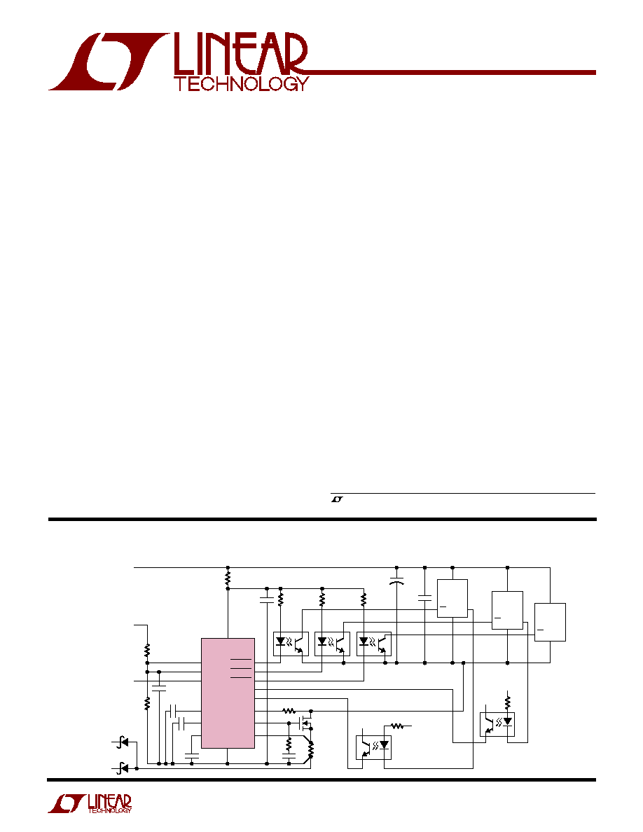
48V Hot Swap Controller
with Sequencer
Hot Swap is a trademark of Linear Technology Corporation.
R4
5.6k
R3
5.6k
R5
5.6k
PWRGD1
V
IN
V
IN
V
EE
LTC4253
POWER
MODULE 1
PWRGD2
PWRGD3
EN3
EN2
OV
UV
RESET
DRAIN
SS
GATE
SQTIMER
SENSE
TIMER
EN
POWER
MODULE 2
EN
POWER
MODULE 3
EN
R
IN
2.8k
16k(1/4W)/6
11
3
4
12
2
5
16
15
1
EN3
4253 TA01
EN2
6
10
14
9
13
7
8
R
C
10
R
D
1M
R
S
0.02
Q1
IRF530S
V
IN
C
C
18nF
C
T
0.33
µ
F
C1 10nF
C
SQ
0.1
µ
F
C
SS
68nF
R6
POWER
MODULE 1
OUTPUT
POWER
MODULE 2
OUTPUT
V
IN
R7
+
C3
0.1
µ
F
C2
100
µ
F
C
IN
1
µ
F
R2
32.4k
1%
B3100*
R1
402k
1%
RESET
48V RTN
(SHORT PIN)
48V A
48V B
(LONG PINS)
48V RTN
(LONG PIN)
B3100*
*DIODES, INC.
MOC207
48V/2.5A Hot Swap Controller
APPLICATIO S
U
FEATURES
DESCRIPTIO
U
TYPICAL APPLICATIO
U
LTC4253
2
4253f
Current into V
IN
(100
µ
s Pulse) ........................... 100mA
Input/Output (Except SENSE
and DRAIN) Voltage ................................... 0.3V to 16V
SENSE Voltage .......................................... 0.6V to 16V
Current Out of SENSE Pin (20
µ
s Pulse) ............ 200mA
V
IN
, DRAIN Pin Minimum Voltage ........................ 0.3V
Current into DRAIN Pin (100
µ
s Pulse) ................. 20mA
Maximum Junction Temperature .......................... 125
°
C
Operating Temperature Range
LTC4253C ............................................... 0
°
C to 70
°
C
LTC4253I ............................................ 40
°
C to 85
°
C
Storage Temperature Range ................. 65
°
C to 150
°
C
Lead Temperature (Soldering, 10 sec).................. 300
°
C
ORDER PART
NUMBER
GN PART
MARKING
T
JMAX
= 125
°
C,
JA
= 130
°
C/W
Consult LTC Marketing for parts specified with wider operating temperature ranges.
4253
4253I
LTC4253CGN
LTC4253IGN
ABSOLUTE AXI U
RATI GS
W
W
W
U
PACKAGE/ORDER I FOR ATIO
U
U
W
(Note 1), All voltages referred to V
EE
ELECTRICAL CHARACTERISTICS
The
q
denotes the specifications which apply over the full operating
temperature range, otherwise specifications are at T
A
= 25
°
C. (Note 2)
SYMBOL
PARAMETER
CONDITIONS
MIN
TYP
MAX
UNITS
V
Z
V
IN
to V
EE
Zener Voltage
I
IN
= 2mA
q
12
13
14.5
V
R
Z
V
IN
to V
EE
Zener Dynamic Impedance
I
IN
= (2mA Thru 30mA)
5
I
IN
V
IN
Supply Current
UV/OV = 4V, V
IN
= (V
Z
0.3V)
q
0.8
2
mA
V
LKO
V
IN
Undervoltage Lockout
Coming Out of UVLO (rising V
IN
)
q
9.2
12
V
V
LKH
V
IN
Undervoltage Lockout Hysteresis
1
V
V
IH
TTL Input High Voltage
q
2
V
V
IL
TTL Input Low Voltage
q
0.8
V
V
HYST
TTL Input Buffer Hysterisis
600
mV
I
LEAK
TTL Input Leakage Current
Input = 0V
q
±
0.1
±
10
µ
A
I
RESET
RESET Input Current
V
EE
V
RESET
V
IN
q
±
0.1
±
10
µ
A
I
EN
EN2, EN3 Input Current
V
EN
= 4V
q
120
180
µ
A
V
EN
= 0V
q
±
0.1
±
10
µ
A
V
SS
SS Voltage
After End of SS Timing Cycle
2.2
V
I
SS
SS Pin Current
UV = OV = 4V, V
SENSE
= V
EE,
V
SS
= 0V (SOURCING)
22
µ
A
UV= OV = 0V, V
SENSE
= V
EE,
V
SS
= 2V (SINKING)
28
mA
R
SS
SS Output Impedance
100
k
V
CB
Circuit Breaker Current Limit Voltage
V
CB
= (V
SENSE
V
EE
)
q
40
50
60
mV
V
ACL
Analog Current Limit Voltage
V
ACL
= (V
SENSE
V
EE
)
q
80
100
120
mV
V
FCL
Fast Current Limit Voltage
V
FCL
= (V
SENSE
V
EE
)
q
150
200
300
mV
V
OS
Analog Current Limit Offset Voltage
10
mV
V
ACL
+ V
OS
Ratio (V
ACL
+ V
OS
) to SS Voltage
0.05
V/V
V
SS
1
2
3
4
5
6
7
8
TOP VIEW
GN PACKAGE
16-LEAD PLASTIC SSOP
16
15
14
13
12
11
10
9
EN2
PWRGD2
PWRGD1
V
IN
RESET
SS
SENSE
V
EE
PWRGD3
EN3
SQTIMER
TIMER
UV
OV
DRAIN
GATE
LTC4253
3
4253f
I
GATE
GATE Pin Output Current
UV = OV = 4V, V
SENSE
= V
EE
,
q
30
50
70
µ
A
V
GATE
= 0V (Sourcing)
UV = OV = 4V, V
SENSE
V
EE
= 0.15V,
17
mA
V
GATE
= 3V (Sinking)
UV = OV = 4V, V
SENSE
V
EE
= 0.3V,
190
mA
V
GATE
= 1V (Sinking)
V
GATE
External MOSFET Gate Drive
V
GATE
V
EE,
I
IN
= 2mA
q
10
12
V
Z
V
V
GATEL
Gate Low Threshold
(Before Gate Ramp Up)
0.5
V
V
GATEH
Gate High Threshold
V
GATEH
= V
IN
V
GATE
,
2.8
V
For PWRGD1, PWRGD2, PWRGD3 Status
V
UVHI
UV Pin Threshold HIGH
q
3.075
3.225
3.375
V
V
UVLO
UV Pin Threshold LOW
q
2.775
2.925
3.075
V
V
UVHST
UV Pin Hysteresis
0.3
V
V
OVHI
OV Pin Threshold HIGH
q
5.85
6.15
6.45
V
V
OVLO
OV Pin Threshold LOW
q
5.55
5.85
6.15
V
V
OVHST
OV Pin Hysteresis
0.3
V
I
SENSE
SENSE Pin Input Current
UV = 0V = 4V, V
SENSE
= 50mV
q
30
15
µ
A
I
INP
UV,OV Pin Input Current
UV = OV = 4V
q
±
0.1
±
10
µ
A
V
TMRH
TIMER Pin Voltage High Threshold
4
V
V
TMRL
TIMER Pin Voltage Low Threshold
1
V
I
TMR
TIMER Pin Current
Timer On (Initial Cycle/Latchoff, Sourcing), V
TMR
= 2V
5
µ
A
Timer Off (Initial Cycle, Sinking), V
TMR
= 2V
28
mA
Timer On (Circuit Breaker, Sourcing,
200
µ
A
I
DRN
= 0
µ
A), V
TMR
= 2V
Timer On (Circuit Breaker, Sourcing,
600
µ
A
I
DRN
= 50
µ
A), V
TMR
= 2V
Timer Off (Circuit Breaker, Sinking), V
TMR
= 2V
5
µ
A
I
TMRACC
(I
TMR
at I
DRN
= 50
µ
A I
TMR
at I
DRN
= 0
µ
A)
Timer On (Circuit Breaker with I
DRN
= 50
µ
A)
8
µ
A/
µ
A
I
DRN
50
µ
A
V
SQTMRH
SQTIMER Pin Voltage High Threshold
4
V
V
SQTMRL
SQTIMER Pin Voltage Low Threshold
0.33
V
I
SQTMR
SQTIMER Pin Current
SQTIMER On (Power Good Sequence, Sourcing),
5
µ
A
V
SQTMR
= 2V
SQTIMER On (Power Good Sequence, Sinking),
28
µ
A
V
SQTMR
= 2V
V
DRNL
DRAIN Pin Voltage Low Threshold
For PWRGD1, PWRGD2, PWRGD3 Status
2.385
V
I
DRNL
DRAIN Leakage Current
V
DRAIN
= 5V
±
0.1
±
1
µ
A
V
DRNCL
DRAIN Pin Clamp Voltage
I
DRN
= 50
µ
A
7
V
V
PGL
PWRGD1, PWRGD2, PWRGD3
I
PG
= 1.6mA
q
0.25
0.4
V
Output Low Voltage
I
PG
= 5mA
q
1.2
V
I
PGH
PWRGD1, PWRGD2, PWRGD3
V
PG
= 0V
q
30
50
70
µ
A
Output High Current
SYMBOL
PARAMETER
CONDITIONS
MIN
TYP
MAX
UNITS
ELECTRICAL CHARACTERISTICS
The
q
denotes the specifications which apply over the full operating
temperature range, otherwise specifications are at T
A
= 25
°
C. (Note 2)
LTC4253
4
4253f
Note 1: Absolute Maximum Ratings are those values beyond which the life
of a device may be impaired.
Note 2: All currents into device pins are positive; all currents out of device
pins are negative. All voltages are referenced to V
EE
unless otherwise
specified.
t
SQ
SQTIMER Default Ramp Period
SQTIMER Pin Floating,
250
µ
s
V
SQTMR
Ramps from 0.5V to 3.5V
t
SS
SS Default Ramp Period
SS Pin Floating, V
SS
Ramps from 0.2V to 2V
250
µ
s
t
PLLUG
UV Low to GATE Low
0.4
µ
s
t
PHLOG
OV High to GATE Low
0.4
µ
s
ELECTRICAL CHARACTERISTICS
The
q
denotes the specifications which apply over the full operating
temperature range, otherwise specifications are at T
A
= 25
°
C. (Note 2)
SYMBOL
PARAMETER
CONDITIONS
MIN
TYP
MAX
UNITS
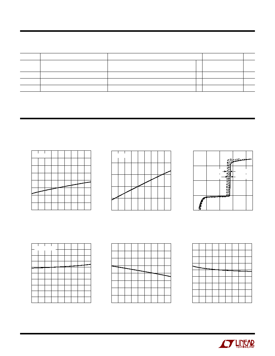
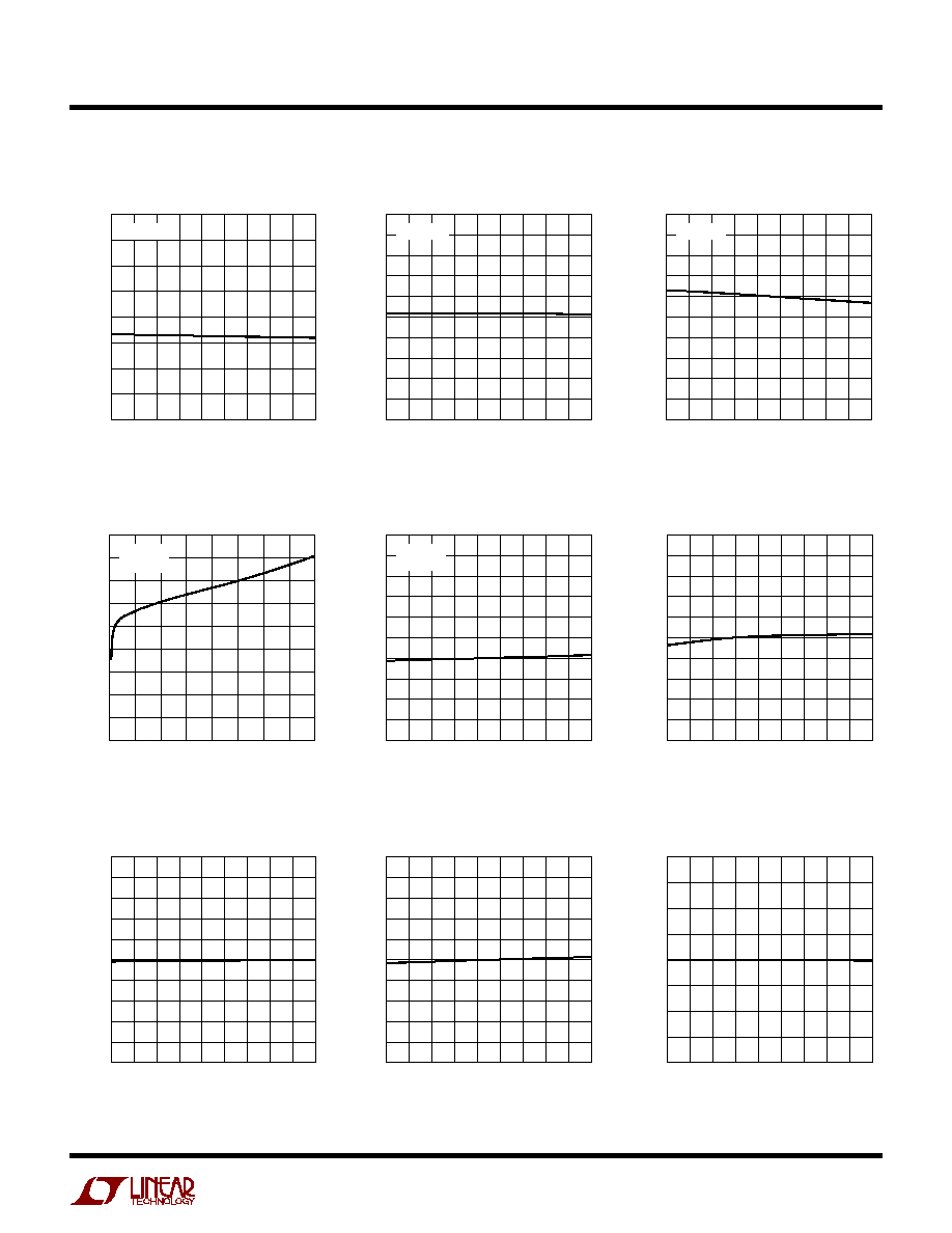
TYPICAL PERFOR A CE CHARACTERISTICS
U
W
I
IN
vs Temperature
I
IN
vs V
IN
r
Z
vs Temperature
V
Z
vs Temperature
Undervoltage Lockout V
LKO
vs
Temperature
Undervoltage Lockout Hysterisis
V
LKH
vs Temperature
TEMPERATURE (
°
C)
55 35 15
5
25
45
65
85 105 125
r
Z
(
)
4253 G01
10
9
8
7
6
5
4
3
2
I
IN
= 2mA
TEMPERATURE (
°
C)
55 35 15
5
25
45
65
85 105 125
V
Z
(V)
4253 G02
14.5
14.0
13.5
13.0
12.5
12.0
I
IN
= 2mA
V
IN
(V)
0
5
10
15
20
I
IN
(mA)
4253 G03
1000
100
10
1
0.1
T
A
= 85
°
C
T
A
= 125
°
C
T
A
= 40
°
C
T
A
= 25
°
C
TEMPERATURE (
°
C)
55 35 15
5
25
45
65
85 105 125
I
IN
(
µ
A)
4253 G04
1000
950
900
850
800
750
700
650
600
550
500
V
IN
= V
Z
0.3V
TEMPERATURE (
°
C)
55 35 15
5
25
45
65
85 105 125
V
LKO
(V)
4253 G05
11.0
10.5
10.0
9.5
9.0
8.5
8.0
7.5
7.0
TEMPERATURE (
°
C)
55 35 15
5
25
45
65
85 105 125
V
LKH
(V)
4253 G06
1.8
1.6
1.4
1.2
1.0
0.8
0.6
0.4
0.2
0
LTC4253
5
4253f
TYPICAL PERFOR A CE CHARACTERISTICS
U
W
Circuit Breaker Current Limit
Voltage V
CB
vs Temperature
Analog Current Limit Voltage V
ACL
vs Temperature
Fast Current Limit Voltage V
FCL
vs
Temperature
V
SS
vs Temperature
V
HYST
vs Temperature
V
IH
vs Temperature
V
IL
vs Temperature
I
EN
(V
EN
= 4V) vs Temperature
I
EN
vs V
EN
TEMPERATURE (
°
C)
55 35 15
5
25
45
65
85 105 125
V
IH
(V)
4253 G07
4.0
3.5
3.0
2.5
2.0
1.5
1.0
0.5
0
I
IN
= 2mA
TEMPERATURE (
°
C)
55 35 15
5
25
45
65
85 105 125
V
IL
(V)
4253 G08
2.0
1.8
1.6
1.4
1.2
1.0
0.8
0.6
0.4
0.2
0
I
IN
= 2mA
TEMPERATURE (
°
C)
55 35 15
5
25
45
65
85 105 125
V
HYST
(V)
4253 G09
1.0
0.9
0.8
0.7
0.6
0.5
0.4
0.3
0.2
0.1
0
I
IN
= 2mA
V
EN
(V)
0
2
4
6
8
10
12
14
16
I
EN
(
µ
A)
4253 G10
180
160
140
120
100
80
60
40
20
0
I
IN
= 2mA
T
A
= 25
°
C
TEMPERATURE (
°
C)
55 35 15
5
25
45
65
85 105 125
I
EN
(
µ
A)
4253 G11
150
145
140
135
130
125
120
115
110
105
100
I
IN
= 2mA
V
EN
= 4V
TEMPERATURE (
°
C)
55 35 15
5
25
45
65
85 105 125
V
CB
(mV)
4253 G12
55
54
53
52
51
50
49
48
47
46
45
TEMPERATURE (
°
C)
55 35 15
5
25
45
65
85 105 125
V
ACL
(mV)
4253 G13
150
140
130
120
110
100
90
80
70
60
50
TEMPERATURE (
°
C)
55 35 15
5
25
45
65
85 105 125
V
FCL
(mV)
4253 G14
300
280
260
240
220
200
180
160
140
120
100
TEMPERATURE (
°
C)
55 35 15
5
25
45
65
85 105 125
V
SS
(V)
4253 G15
2.40
2.35
2.30
2.25
2.20
2.15
2.10
2.05
2.00