 | ÐлекÑÑоннÑй компоненÑ: LTC4255CG | СкаÑаÑÑ:  PDF PDF  ZIP ZIP |
Äîêóìåíòàöèÿ è îïèñàíèÿ www.docs.chipfind.ru
LTC4255
1
4255f
s
Controls Four Independent 48V Power Channels
s
Each Channel has Separate Relay Drivers, ON/OFF
Control, Short-Circuit Protection with Current
Foldback, Open-Circuit Detection, and Power Good
Indication
s
Programmed via I
2
C
TM
Compatible Interface
s
Five Bit Programmable Digital Address Allows
Control of up to 32 LTC4255s (128 Channels)
s
Interrupt on FAULT Output can be used to Eliminate
Software Polling
s
Programmable Current Limit and Open-Circuit
Duration Periods
s
Programmable Latchoff or Autoretry after Short-
Circuit Faults
s
Programmable Autoretry Duty Cycle
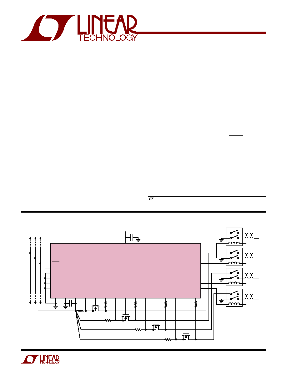
Quad Network Power
Controller with I
2
C Compatible Interface
The LTC
®
4255 is a quad 48V network power controller
with independent relay drivers and I
2
C compatible inter-
face. Each channel can be turned on and off via software
control, while providing short-circuit protection, open-
circuit detection, and power good indication. The short-
circuit protection includes a current foldback feature to
reduce power dissipation in the switch during shorts and
start-up.
The serial interface allows up to 128 channels to be
controlled with only two digital lines. A FAULT output can
be used as an interrupt line to eliminate fault detection by
software polling.
External switches and current sense resistors allow easy
scaling of current and power dissipation levels and pro-
vide the maximum protection against voltage and current
spikes.
The LTC4255 is available in the 28-pin SSOP package.
, LTC and LT are registered trademarks of Linear Technology Corporation.
R
S1
0.33
R
S2
0.33
R
S3
0.33
R
S4
0.33
Q1
Q2
Q3
Q4
12V
0.1
µ
F
48V
4255 TA01
100k
100k
100k
100k
SCL
SDA
FAULT
AD0
AD1
AD2
AD3
AD4
DGND AGND
V
EE
SENSE1 GATE1
OUT1 SENSE2 GATE2
OUT2 SENSE3 GATE3
OUT3 SENSE4 GATE4 OUT4
RELAY1
RELAY2
RELAY3
RELAY4
LTC4255
V
CC
0.1
µ
F
Q1, Q2, Q3, Q4: FDC3612
RELAYS: V23079 SERIES
s
IP Phone Systems
s
DTE Power Distribution
I
2
C is a trademark of Philips Electronics N.V.
FEATURES
DESCRIPTIO
U
APPLICATIO S
U
TYPICAL APPLICATIO
U
LTC4255
2
4255f
Supply Voltages
V
CC
to DGND ....................................................... 18V
V
EE
to AGND ...................................................... 80V
DGND to AGND ...................................................
±
5V
Digital Pin Voltages
SCL, SDA, FAULT ........................ DGND 0.3V to 6V
AD0-4 ....................................... DGND 0.3V to 5.5V
Relay Driver Output Voltage
RELAY1-4 (Note 5) ...... DGND 0.3V to DGND + 15V
Analog Voltages
SENSE1-4 ............................... V
EE
0.3V to V
EE
+ 1V
OUT1-4 .................................. V
EE
80V to V
EE
+ 80V
Operating Temperature Range
LTC4255C ............................................... 0
°
C to 70
°
C
Storage Temperature Range ................. 65
°
C to 150
°
C
Lead Temperature (Soldering, 10 sec).................. 300
°
C
ORDER PART
NUMBER
T
JMAX
= 125
°
C,
JA
= 90
°
C/W
LTC4255CG
ABSOLUTE AXI U
RATI GS
W
W
W
U
PACKAGE/ORDER I FOR ATIO
U
U
W
(Note 1)
ELECTRICAL CHARACTERISTICS
The
q
denotes the specifications which apply over the full operating
temperature range, otherwise specifications are at T
A
= 25
°
C. V
CC
= 12V, V
EE
= 48V, AGND = DGND = 0V (Note 2)
Consult LTC Marketing for parts specified with wider operating temperature ranges.
1
2
3
4
5
6
7
8
9
10
11
12
13
14
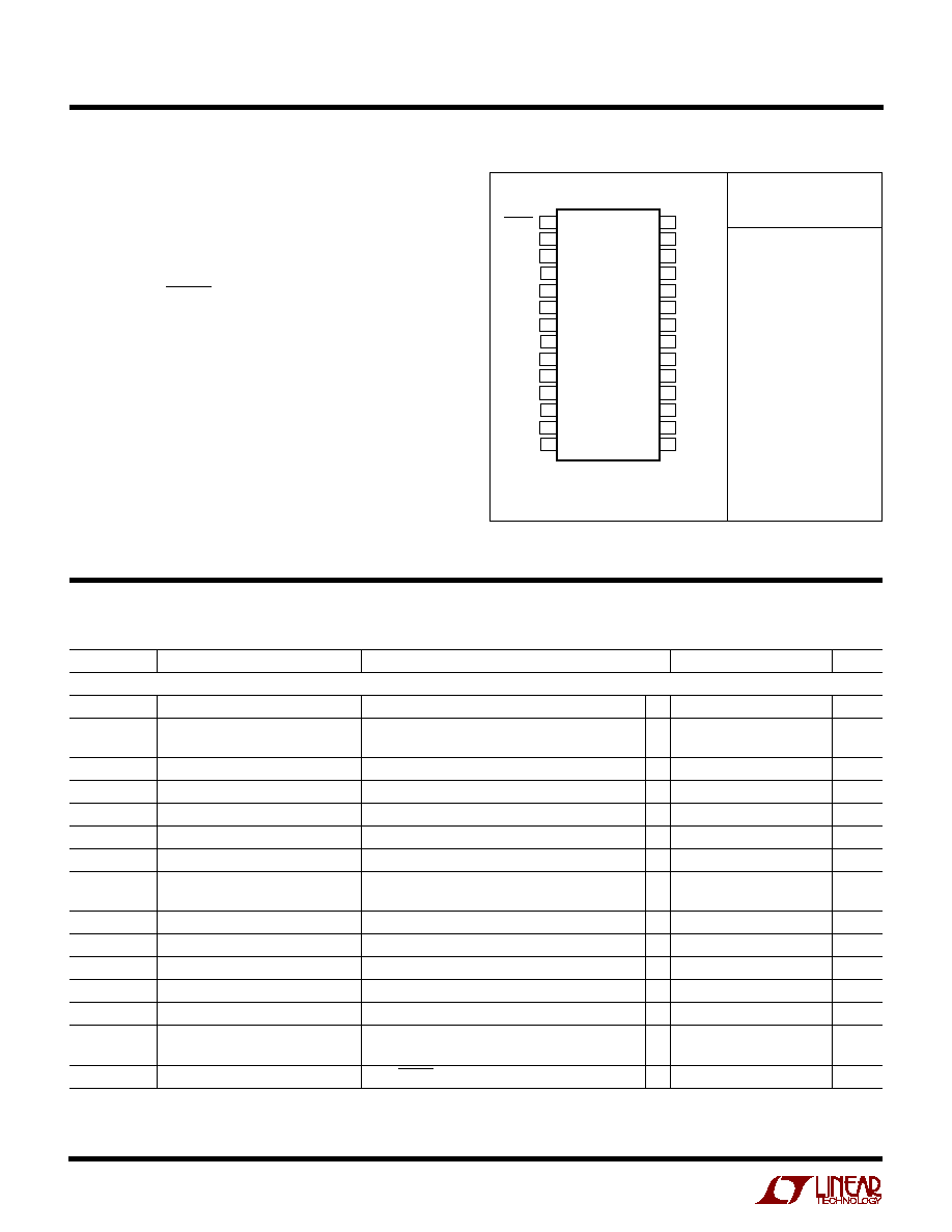
TOP VIEW
G PACKAGE
28-LEAD PLASTIC SSOP
28
27
26
25
24
23
22
21
20
19
18
17
16
15
OUT1
GATE1
SENSE1
OUT2
GATE2
SENSE2
V
EE
OUT3
GATE3
SENSE3
OUT4
GATE4
SENSE4
AGND
FAULT
SCL
SDA
AD4
AD3
AD2
AD1
AD0
RELAY1
RELAY2
RELAY3
RELAY4
DGND
V
CC
SYMBOL
PARAMETER
CONDITIONS
MIN
TYP
MAX
UNITS
DC Characteristics
V
CC
Positive Supply Voltage
V
CC
Referenced to DGND
10.8
12
13.2
V
I
CC
Positive Supply Current
Relays Off
2.1
3
mA
All Relays On
10
15
mA
V
EE
Negative Supply Voltage
V
EE
Referenced to AGND
48
72
V
I
EE
Negative Supply Current
1.9
3
mA
V
GND
DC Ground Difference
AGND DGND (Note 3)
5
5
V
V
LKO
V
EE
Undervoltage Lockout
27
V
V
GATE
External Gate Voltage (V
GATE
V
EE
)
I
GATE
= 1
µ
A
10
13
15
V
I
GATE
GATE Pin Output Current
GATE On, V
GATE
= V
EE
30
50
70
µ
A
GATE Off, V
GATE
= V
EE
+ 5V
30
50
80
µ
A
V
SC
Short-Circuit Sense Voltage
(V
SENSE
V
EE
), V
OUT
V
EE
= 0V
q
125
150
170
mV
V
OC
Open-Circuit Sense Voltage
(V
SENSE
V
EE
)
q
1
3
4.5
mV
V
PG
Power_OK Threshold Voltage
(V
OUT
V
EE
)
q
1
2
3
V
I
OUT
OUT Pin Current
V
OUT
= V
EE
1.4
µ
A
V
OLR
Relay Driver Output Low Voltage
(V
RELAY
DGND), I
RELAY
= 50mA, RELAY On
0.3
V
V
CLAMPR
Relay Driver Clamp Voltage
(V
RELAY
DGND), I
RELAY
= 50mA,
18
24
V
RELAY Off (Note 5)
V
OLD
Digital Output Low Voltage
SDA, FAULT, I = 3mA
q
0.4
V
LTC4255
3
4255f
ELECTRICAL CHARACTERISTICS
The
q
denotes the specifications which apply over the full operating
temperature range, otherwise specifications are at T
A
= 25
°
C. V
CC
= 12V, V
EE
= 48V, AGND = DGND = 0V
SYMBOL
PARAMETER
CONDITIONS
MIN
TYP
MAX
UNITS
V
ILD
Digital Input Low Voltage
SCL, SDA
q
0.8
V
V
IHD
Digital Input High Voltage
SCL, SDA
q
2.4
V
R
PU
AD0 to AD4 Pullup Resistors to 5V
30
50
90
k
AC Characteristics
t
CL
Current Limit Filter Time
B5 = 0, B4 = 0, Figure 2
q
4.8
6
7.2
ms
B5 = 0, B4 = 1
q
9.6
12
14.4
ms
B5 = 1, B4 = 0
q
19.2
24
28.8
ms
B5 = 1, B4 = 1
q
76.8
96
115.2
ms
t
OCD
Open-Circuit Enable Delay
B7 = 0, B6 = 0
q
50
62
74
ms
After Power_OK
B7 = 0, B6 = 1
q
104
130
156
ms
B7 = 1, B6 = 0
q
213
267
320
ms
B7 = 1, B6 = 1
q
433
541
649
ms
t
OCF
Open-Circuit Filter Time
Figure 3
q
9.6
18
28.8
ms
t
OD
Turn-On Delay Time
Figure 4
q
9.6
18
28.8
ms
DC
R
Retry Duty Cycle
B3 = 0
q
0.78
0.83
0.89
%
B3 = 1
q
5.5
6
6.7
%
t
SCLK
Clock Frequency
(Note 3)
q
400
kHz
t
1
Bus Free Time
Figure 1 (Notes 3, 4)
q
1.3
µ
s
t
2
Start Hold Time
Figure 1 (Notes 3, 4)
q
600
ns
t
3
SCL Low Time
Figure 1 (Notes 3, 4)
q
1.3
µ
s
t
4
SCL High Time
Figure 1 (Notes 3, 4)
q
600
ns
t
5
Data Hold Time
Figure 1 (Notes 3, 4)
q
150
ns
t
6
Data Setup Time
Figure 1 (Notes 3, 4)
q
200
ns
t
7
Start Setup Time
Figure 1 (Notes 3, 4)
q
600
ns
t
8
Stop Setup Time
Figure 1 (Notes 3, 4)
q
600
ns
t
9
Stop to Fault Clear
Figure 1 (Notes 3, 4)
q
300
ns
t
r
SCL, SDA Rise Time
Figure 1 (Notes 3, 4)
q
20
300
ns
t
f
SCL, SDA Fall Time
Figure 1 (Notes 3, 4)
q
20
150
ns
Note 1: Absolute Maximum Ratings are those values beyond which the life
of a device may be impaired.
Note 2: All currents into device pins are positive; all currents out of device
pins are negative. All voltages are referenced to ground unless otherwise
specified.
Note 3: Guaranteed by design, not subject to test.
Note 4: Values referred to V
ILD
and V
IHD
.
Note 5: A Zener diode clamps the relay drivers at 18V (RELAY 1-4).
LTC4255
4
4255f
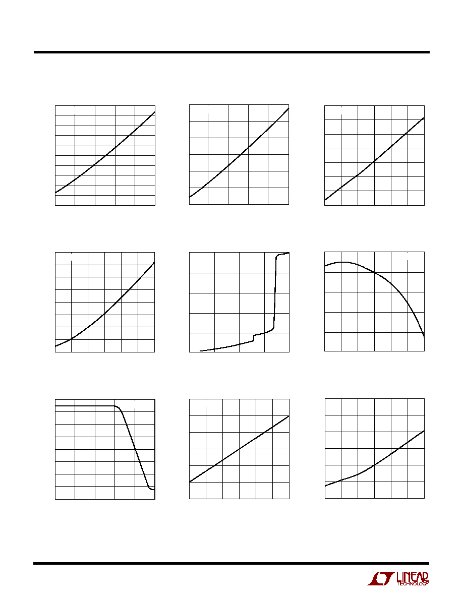
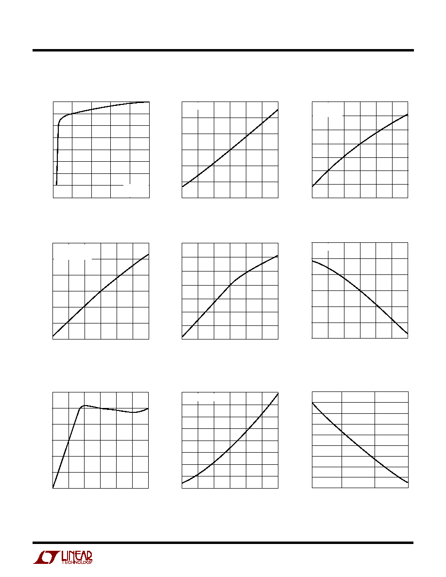
TYPICAL PERFOR A CE CHARACTERISTICS
U
W
I
CC
vs V
CC
(Relays Off)
V
CC
(V)
10.8
I
CC
(mA)
1.280
1.270
1.290
12.8
4255 G01
1.260
1.250
1.240
11.3
11.8
12.3
13.3
T
A
= 25
°
C
I
CC
vs V
CC
(Relays On)
V
CC
(V)
10.8
8.6
I
CC
(mA)
8.8
9.0
9.2
9.4
9.6
9.8
11.3
11.8
12.3
12.8
4255 G02
13.3
T
A
= 25
°
C
TEMPERATURE (
°
C)
50
I
CC
(mA)
1.28
1.30
1.32
75
50
4255 G03
1.26
1.24
25
0
25
100
1.22
1.20
1.34
V
CC
= 12V
I
CC
vs Temperature (Relays Off)
I
CC
vs Temperature (Relays On)
I
EE
vs V
EE
I
EE
vs Temperature
TEMPERATURE (
°
C)
50
I
CC
(mA)
9.2
9.3
9.4
75
50
4255 G04
9.1
9.0
25
0
25
100
8.9
8.8
9.6
9.5
V
CC
= 12V
V
EE
(V)
2.0
I
EE
(mA)
1.6
1.2
0.8
0.4
0
80
60
40
4255 G05
20
0
T
A
= 25
°
C
TEMPERATURE (
°
C)
50
1.98
I
EE
(mA)
1.96
1.94
1.92
1.90
1.88
25
0
25
50
4255 G06
75
100
V
EE
= 48V
V
SC
vs V
OUT
V
SC
vs Temperature
V
OC
vs Temperature
V
OUT
(V)
50
V
SC
(mV)
60
80
100
30
10
4255 G07
40
20
0
40
20
120
140
160
0
T
A
= 25
°
C
TEMPERATURE (
°
C)
50
135
V
SC
(mV)
140
145
150
155
165
25
0
25
50
4255 G08
75
100
160
V
OUT
= V
EE
TEMPERATURE (
°
C)
50
2.90
V
OC
(mV)
3.00
3.10
25
0
25
50
4255 G09
75
3.20
2.95
3.05
3.15
100
LTC4255
5
4255f
TYPICAL PERFOR A CE CHARACTERISTICS
U
W
I
OUT
vs V
OUT
I
OUT
vs Temperature
I
GATE
vs Temperature
I
GATE
vs Temperature
I
SENSE
vs Temperature
V
EE
Undervoltage Lockout
vs Temperature
Relay Driver Output Low Voltage
(V
OLR
) vs Temperature
V
OUT
(V)
50
I
OUT
(
µ
A)
1.0
0.8
0.6
30
10
4255 G10
1.2
1.4
1.6
40
20
0.4
0.2
0
0
T
A
= 25
°
C
V
EE
= 48V
TEMPERATURE (
°
C)
50
0.8
I
OUT
(
µ
A)
1.0
1.2
1.4
1.6
2.0
25
0
25
50
4255 G11
75
100
1.8
V
OUT
= V
EE
TEMPERATURE (
°
C)
50
44
46
48
50
52
54
56
58
25
75
4255 G12
25
0
50
100
I
GATE
(
µ
A)
GATE ON
V
GATE
= V
EE
TEMPERATURE (
°
C)
50
35
I
GATE
(
µ
A)
40
45
50
55
65
25
0
25
50
4255 G13
75
100
60
GATE OFF
V
GATE
= V
EE
+ 5V
V
GATE
vs Temperature
TEMPERATURE (
°
C)
50
13.6
13.4
13.2
13.0
12.8
12.6
12.4
12.2
25
75
4255 G14
25
0
50
100
V
GATE
(V)
TEMPERATURE (
°
C)
50
48
I
SENSE
(
µ
A)
47
46
45
44
42
25
0
25
50
4255 G15
75
100
43
V
SENSE
= V
EE
TEMPERATURE (
°
C)
50
32
V
EE
UNDERVOLTAGE LOCKOUT (V)
31
30
29
28
26
25
0
25
50
4255 G16
75
100
27
AD0-4 Pullup Resistors to 5V (R
PU
)
vs Temperature
TEMPERATURE (
°
C)
50
V
OL
(V)
0.150
0.160
100
4255 G17
0.140
0.130
25
25
0
50
75
0.170
0.145
0.155
0.135
0.165
I
RELAY
= 50mA
TEMPERATURE (
°
C)
51
R
PU
(k
)
52
54
55
56
0
100
60
4255 G18
53
50
50
57
58
59