Äîêóìåíòàöèÿ è îïèñàíèÿ www.docs.chipfind.ru
LTC4300-1/LTC4300-2
1
sn430012 430012fs
The LTC
®
4300 series hot swappable 2-wire bus buffers
allow I/O card insertion into a live backplane without cor-
ruption of the data and clock busses. When the connection
is made, the LTC4300-1/LTC4300-2 provide bidirectional
buffering, keeping the backplane and card capacitances
isolated. Rise-time accelerator circuitry* allows the use of
weaker DC pull-up currents while still meeting rise-time
requirements. During insertion, the SDA and SCL lines are
precharged to 1V to minimize bus disturbances.
The LTC4300-1 incorporates a CMOS threshold digital
ENABLE input pin, which forces the part into a low current
mode when driven to ground and sets normal operation when
driven to V
CC
. It also includes an open drain READY output
pin, which indicates that the backplane and card sides are
connected together. The LTC4300-2 replaces the ENABLE
pin with a dedicated supply voltage pin, V
CC2
, for the card
side, providing level shifting between 3.3V and 5V systems.
Both the backplane and card may be powered with supply
voltages ranging from 2.7V to 5.5V, with no contraints on
which supply voltage is higher. The LTC4300-2 also replaces
the READY pin with a digital CMOS input pin, ACC, which
enables and disables the rise-time accelerator currents.
The LTC4300 is available in a small 8-pin MSOP package.
s
Hot Board Insertion
s
Servers
s
Capacitance Buffer/Bus Extender
s
Desktop Computer
, LTC and LT are registered trademarks of Linear Technology Corporation.
s
Bidirectional Buffer for SDA and SCL Lines
Increases Fanout
s
Prevents SDA and SCL Corruption During Live
Board Insertion and Removal from Backplane
s
Isolates Input SDA and SCL Lines from Output
s
Compatible with I
2
C
TM
, I
2
C Fast Mode and SMBus
Standards (Up to 400kHz Operation)
s
Small MSOP 8-Pin Package
s
Low I
CC
Chip Disable: <1
µ
A (LTC4300-1)
s
READY Open Drain Output (LTC4300-1)
s
1V Precharge on all SDA and SCL Lines
s
Supports Clock Stretching, Arbitration and
Synchronization
s
5V to 3.3V Level Translation (LTC4300-2)
s
High Impedance SDA, SCL Pins for V
CC
= 0V
Hot Swappable
2-Wire Bus Buffers
I
2
C is a trademark of Philips Electronics N. V.
*U.S. Patent No. 6,650,174
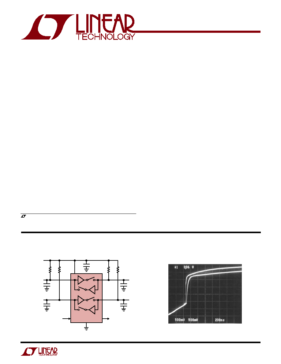
R1
24k
V
CC
3.3V
R2
24k
ENABLE
SCLIN
SCLOUT
SDAIN
SDAOUT
1
5
4
6
7
3
2
8
GND
LTC4300-1
READY
C1
0.01
µ
F
C2*
C4*
C5*
C3*
4300-1/2 TA01
R3
24k
R4
24k
*CAPACITORS NOT REQUIRED
IF BUS IS SUFFICIENTLY LOADED
APPLICATIO S
U
FEATURES
TYPICAL APPLICATIO
U
DESCRIPTIO
U
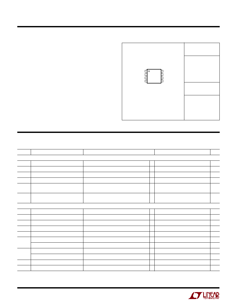
InputOutput Connection t
PLH
OUTPUT
SIDE
50pF
INPUT
SIDE
150pF
LTC4300-1/LTC4300-2
2
sn430012 430012fs
V
CC
to GND .................................................... 0.5 to 7V
V
CC2
to GND (LTC4300-2) ............................. 0.5 to 7V
SDAIN, SCLIN, SDAOUT, SCLOUT ................. 0.5 to 7V
READY, ENABLE (LTC4300-1) ....................... 0.5 to 7V
ACC (LTC4300-2) .......................................... 0.5 to 7V
Operating Temperature Range
LTC4300-1C/LTC4300-2C ....................... 0
°
C to 70
°
C
LTC4300-1I/LTC4300-2I .................... 40
°
C to 85
°
C
Storage Temperature Range ................. 65
°
C to 125
°
C
Lead Temperature (Soldering, 10 sec).................. 300
°
C
ORDER PART
NUMBER
MS8
PART MARKING
T
JMAX
= 125
°
C,
JA
= 200
°
C/W
Consult LTC marketing for parts specified with wider operating temperature ranges.
LTUB
LTUC
LTVJ
LTVK
LTC4300-1CMS8
LTC4300-1IMS8
LTC4300-2CMS8
LTC4300-2IMS8
ABSOLUTE AXI U
RATI GS
W
W
W
U
PACKAGE/ORDER I FOR ATIO
U
U
W
(Note 1)
ELECTRICAL CHARACTERISTICS
The
q
denotes the specifications which apply over the full operating
temperature range, otherwise specfications are at T
A
= 25
°
C. V
CC
= 2.7V to 5.5V, unless otherwise noted.
1
2
3
4
ENABLE/V
CC2
*
SCLOUT
SCLIN
GND
8
7
6
5
V
CC
SDAOUT
SDAIN
READY/ACC*
TOP VIEW
MS8 PACKAGE
8-LEAD PLASTIC MSOP
*LTC4300-2
SYMBOL PARAMETER
CONDITIONS
MIN
TYP
MAX
UNITS
Power Supply
V
CC
Positive Supply Voltage
q
2.7
5.5
V
I
CC
Supply Current
V
CC
= 5.5V, V
SDAIN
= V
SCLIN
= 0V, LTC4300-1
q
2.8
6
mA
I
SD
Supply Current in Shutdown Mode
V
ENABLE
= 0V, LTC4300-1
0.1
µ
A
V
CC2
Card Side Supply Voltage
LTC4300-2
q
2.7
5.5
V
I
VCC1
V
CC
Supply Current
V
SDAIN
= V
SCLIN
= 0V, V
CC1
= V
CC2
= 5.5V,
1.8
3.6
mA
LTC4300-2
I
VCC2
V
CC2
Supply Current
V
SDAOUT
= V
SCLOUT
= 0V, V
CC1
= V
CC2
= 5.5V,
1.2
2.4
mA
LTC4300-2
Start-Up Circuitry
V
PRE
Precharge Voltage
SDA, SCL Floating
q
0.8
1.0
1.2
V
t
IDLE
Bus Idle Time
q
50
95
150
µ
s
V
EN
ENABLE Threshold Voltage
LTC4300-1
0.5 · V
CC
0.9 · V
CC
V
V
DIS
Disable Threshold Voltage
LTC4300-1, ENABLE Pin
0.1 · V
CC
0.5 · V
CC
V
I
EN
ENABLE Input Current
ENABLE from 0V to V
CC
, LTC4300-1
±
0.1
±
1
µ
A
t
PHL
ENABLE Delay, On-Off
LTC4300-1
100
ns
READY Delay, Off-On
LTC4300-1
10
ns
t
PLH
ENABLE Delay, Off-On
LTC4300-1
80
µ
s
READY Delay, On-Off
LTC4300-1
10
µ
s
I
OFF
READY OFF State Leakage Current
LTC4300-1
±
0.1
µ
A
V
OL
READY Output Low Voltage
I
PULLUP
= 3mA, LTC4300-1
q
0.4
V
LTC4300-1/LTC4300-2
3
sn430012 430012fs
Note 1: Absolute Maximum Ratings are those values beyond which the life
of a device may be impaired
Note 2: I
PULLUPAC
varies with temperature and V
CC
voltage, as shown in
the Typical Performance Characteristics section.
Note 3: The connection circuitry always regulates its output to a higher
voltage than its input. The magnitude of this offset voltage as a function of
the pullup resistor and V
CC
voltage is shown in the Typical Performance
Characteristics section.
ELECTRICAL CHARACTERISTICS
The
q
denotes the specifications which apply over the full operating
temperature range, otherwise specfications are at T
A
= 25
°
C. V
CC
= 2.7V to 5.5V, unless otherwise noted.
SYMBOL PARAMETER
CONDITIONS
MIN
TYP
MAX
UNITS
Rise-Time Accelerators
I
PULLUPAC
Transient Boosted Pull-Up Current
Positive Transition on SDA,SCL, V
CC
= 2.7V,
1
2
mA
Slew Rate = 1.25V/
µ
s (Note 2),
LTC4300-2, ACC = 0.7 · V
CC2
, V
CC2
= 2.7V
V
ACCDIS
Accelerator Disable Threshold
LTC4300-2
0.3 · V
CC2
0.5 · V
CC2
V
V
ACCEN
Accelerator Enable Threshold
LTC4300-2
0.5 · V
CC2
0.7 · V
CC2
V
I
VACC
ACC Input Current
LTC4300-2
±
0.1
±
1
µ
A
t
PDOFF
ACC Delay, On/Off
LTC4300-2
5
ns
Input-Output Connection
V
OS
Input-Output Offset Voltage
10k to V
CC
on SDA, SCL, V
CC
= 3.3V (Note 3),
q
0
75
150
mV
LTC4300-2, V
CC2
= 3.3V, V
IN
= 0.2V
f
SCL, SDA
Operating Frequency
Guaranteed by Design, Not Subject to Test
0
400
kHz
C
IN
Digital Input Capacitance
Guaranteed by Design, Not Subject to Test
10
pF
V
OL
Output Low Voltage, Input = 0V
SDA, SCL Pins, I
SINK
= 3mA, V
CC
= 2.7V,
q
0
0.4
V
V
CC2
= 2.7V, LTC4300-2
I
LEAK
Input Leakage Current
SDA, SCL Pins = V
CC
= 5.5V,
±
5
µ
A
LTC4300-2, V
CC2
= 5.5V
Timing Characteristics
f
I2C
I
2
C Operating Frequency
(Note 4)
0
400
kHz
t
BUF
Bus Free Time Between Stop
(Note 4)
1.3
µ
s
and Start Condition
t
hD,STA
Hold Time After (Repeated)
(Note 4)
0.6
µ
s
Start Condition
t
su,STA
Repeated Start Condition Setup Time
(Note 4)
0.6
µ
s
t
su,STO
Stop Condition Setup Time
(Note 4)
0.6
µ
s
t
hD, DAT
Data Hold Time
(Note 4)
300
ns
t
su, DAT
Data Setup Time
(Note 4)
100
ns
t
LOW
Clock Low Period
(Note 4)
1.3
µ
s
t
HIGH
Clock High Period
(Note 4)
0.6
µ
s
t
f
Clock, Data Fall Time
(Notes 4, 5)
20 + 0.1 · C
B
300
ns
t
r
Clock, Data Rise Time
(Notes 4, 5)
20 + 0.1 · C
B
300
ns
Note 4: Guaranteed by design, not subject to test.
Note 5: C
B
= total capacitance of one bus line in pF.
LTC4300-1/LTC4300-2
4
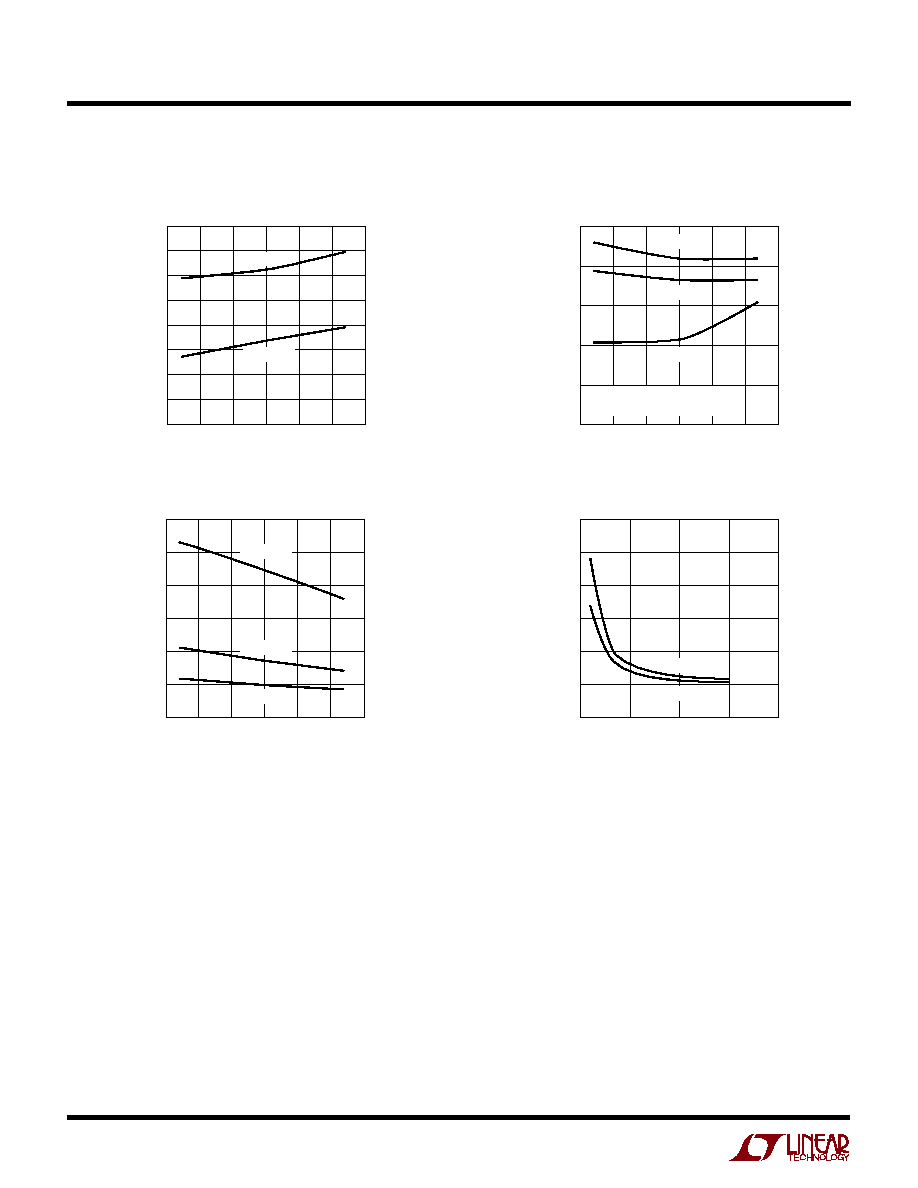
sn430012 430012fs
50
25
0
25
50
75
100
TEMPERATURE (
°
C)
I
PULLUPAC
(mA)
4300-1/2 G03
12
10
8
6
4
2
0
V
CC
= 2.7V
V
CC
= 5V
V
CC
= 3V
R
PULLUP
(
)
0
10,000
20,000
30,000
40,000
V
OUT
V
IN
(mV)
4300-1/2 G04
300
250
200
150
100
50
0
V
CC
= 3.3V
V
CC
= 5V
T
A
= 25
°
C
V
IN
= 0V
I
PULLUPAC
vs Temperature
Connection Circuitry V
OUT
V
IN
TYPICAL PERFOR A CE CHARACTERISTICS
U
W
50
25
0
25
50
75
100
TEMPERATURE (
°
C)
t
PHL
(ns)
4300-1/2 G02
100
80
60
40
20
0
V
CC
= 2.7V
V
CC
= 3.3V
V
CC
= 5.5V
C
IN
= C
OUT
= 100pF
R
PULLUPIN
= R
PULLUPOUT
= 10k
Input Output t
PHL
vs Temperature
(LTC4300-1)
50
25
0
25
50
75
100
TEMPERATURE (
°
C)
I
CC
(mA)
4300-1/2 G01
3.0
2.9
2.8
2.7
2.6
2.5
2.4
2.3
2.2
V
CC
= 5.5V
V
CC
= 2.7V
I
CC
vs Temperature (LTC4300-1)

LTC4300-1/LTC4300-2
5
sn430012 430012fs
ENABLE/V
CC2
(Pin 1): Chip Enable Pin/Card Supply Volt-
age. For the LTC4300-1, this is a digital CMOS threshold
input pin. Grounding this pin puts the part in a low current
(<1
µ
A) mode. It also disables the rise-time accelerators,
disables the bus precharge circuitry, drives READY low,
isolates SDAIN from SDAOUT and isolates SCLIN from
SCLOUT. Drive ENABLE all the way to V
CC
for normal
operation. Connect ENABLE to V
CC
if this feature is not
being used. For the LTC4300-2, this is the supply voltage
for the devices on the card I
2
C busses. Connect pull-up
resistors from SDAOUT and SCLOUT to this pin. Place a
bypass capacitor of at least 0.01
µ
F close to this pin for best
results.
SCLOUT (Pin 2): Serial Clock Output. Connect this pin to
the SCL bus on the card. See Figures 3 and 4 for bus pull-
up resistance and capacitance requirements.
SCLIN (Pin 3): Serial Clock Input. Connect this pin to the
SCL bus on the backplane. See Figures 3 and 4 for bus pull-
up resistance and capacitance requirements.
GND (Pin 4): Ground. Connect this pin to a ground plane
for best results.
READY/ACC (Pin 5): Connection Flag/Rise-Time Accel-
erator Control. For the LTC4300-1, this is an open-drain
NMOS output which pulls low when either ENABLE is low
or the start-up sequence described in the Operation sec-
tion has not been completed. READY goes high when
ENABLE is high and start-up is complete. Connect a 10k
resistor from this pin to V
CC
to provide the pull up. For the
LTC4300-2, this is a CMOS threshold digital input pin that
enables and disables the rise-time accelerators on all four
SDA and SCL pins. Drive ACC all the way to the V
CC2
supply
voltage to enable all four accelerators; drive ACC to ground
to turn them off.
SDAIN (Pin 6): Serial Data Input. Connect this pin to the
SDA bus on the backplane. See Figures 3 and 4 for bus
pull-up resistance and capacitance requirements.
SDAOUT (Pin 7): Serial Data Output. Connect this pin to
the SDA bus on the card. See Figures 3 and 4 for bus pull-
up resistance and capacitance requirements.
V
CC
(Pin 8): Main Input Power Supply from Backplane.
This is the supply voltage for the devices on the backplane
I
2
C busses. Connect pull-up resistors from SDAIN and
SCLIN to this pin. Place a bypass capacitor of at least
0.01
µ
F close to this pin for best results.
PI FU CTIO S
U
U
U