Äîêóìåíòàöèÿ è îïèñàíèÿ www.docs.chipfind.ru
1
LTC4301L
4301lf
FEATURES
DESCRIPTIO
U
APPLICATIO S
U
TYPICAL APPLICATIO
U
Hot Swappable 2-Wire
Bus Buffer with Low Voltage
Level Translation
s
Level Translates 1V Signals to Standard 3.3V and
5V Logic Rails
s
Allows Bus Pull-Up Voltages as Low as 1V on
SDAIN and SCLIN
s
Bidirectional Buffer* for SDA and SCL Lines
Increases Fanout
s
Prevents SDA and SCL Corruption During Live Board
Insertion and Removal from Backplane
s
Isolates Input SDA and SCL Line from Output
s
10kV Human Body Model ESD Protection
s
Supports Clock Stretching, Arbitration and
Synchronization
s
High Impedance SDA, SCL Pins for V
CC
= 0V
s
CS Gates Connection from Input to Output
s
Compatible with I
2
C
TM
, I
2
C Fast Mode and SMBus
Standards (Up to 400kHz Operation)
s
Small 8-Pin MSOP and DFN (3mm
×
3mm) Packages
s
Hot Board Insertion
s
Servers
s
Capacitance Buffer/Bus Extender
s
Desktop Computers
, LTC and LT are registered trademarks of Linear Technology Corporation.
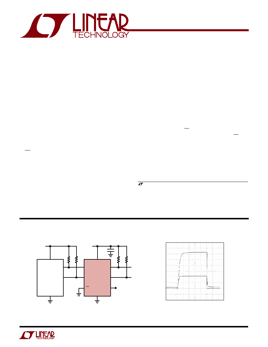
The LTC
®
4301L hot swappable, 2-wire bus buffer allows
I/O card insertion into a live backplane without corruption
of the data and clock busses. In addition, the LTC4301L
SDAIN and SCLIN pins are compatible with systems with
pull-up voltages as low as 1V. Control circuitry prevents
the backplane from being connected to the card until a
stop bit or a bus idle is present. When the connection is
made, the LTC4301L provides bidirectional buffering,
keeping the backplane and card capacitances isolated.
When driven low, the CS input pin allows the part to
connect after a stop bit or bus idle occurs. Driving CS high
breaks the connection between SCLIN and SCLOUT and
between SDAIN and SDAOUT. A logic high on READY
indicates that the backplane and card sides are connected
together.
The LTC4301L is offered in 8-pin DFN (3mm
×
3mm) and
MSOP packages.
Input-Output Connection
OUTPUT
SIDE
20pF
INPUT
SIDE
55pF
4301 TA01b
1
µ
s/DIV
0.5V/DIV
µ
P
SDA
SCL
V
CC
GND
SDAIN
SCLIN
CS
SDAOUT
SCLOUT
READY
LTC4301L
V
CC
GND
2k
10k
2k
10k
0.01
µ
F
SDA
SCL
1.2V
3.3V
4301l TA01a
I
2
C is a trademark of Philips Electronics N.V.
*Patent Pending
2
LTC4301L
4301lf
ORDER PART
NUMBER
V
CC
to GND ................................................. 0.3V to 7V
SDAIN, SCLIN, SDAOUT, SCLOUT, CS ........ 0.3V to 7V
READY ........................................................ 0.3V to 6V
Operating Temperature Range
LTC4301LC ............................................. 0
°
C to 70
°
C
LTC4301LI .......................................... 40
°
C to 85
°
C
LTC4301LCDD8
LTC4301LIDD8
T
JMAX
= 125
°
C,
JA
= 43
°
C/W
EXPOSED PAD (PIN 9) IS GND
PCB CONNECTION OPTIONAL
ABSOLUTE
M
AXI
M
U
M
RATINGS
W
W
W
U
PACKAGE/ORDER I
N
FOR
M
ATIO
N
W
U
U
DD8 PART
MARKING
LBHS
Consult LTC Marketing for parts specified with wider operating temperature ranges.
Storage Temperature Range
MSOP ............................................... 65
°
C to 150
°
C
DFN .................................................. 65
°
C to 125
°
C
Lead Temperature (Soldering, 10 sec).................. 300
°
C
(Note 1)
ORDER PART
NUMBER
LTC4301LCMS8
LTC4301LIMS8
MS8 PART
MARKING
LTBHQ
TOP VIEW
9
DD8 PACKAGE
8-LEAD (3mm
×
3mm) PLASTIC DFN
5
6
7
8
4
3
2
1
CS
SCLOUT
SCLIN
GND
V
CC
SDAOUT
SDAIN
READY
T
JMAX
= 125
°
C,
JA
= 200
°
C/W
1
2
3
4
CS
SCLOUT
SCLIN
GND
8
7
6
5
V
CC
SDAOUT
SDAIN
READY
TOP VIEW
MS8 PACKAGE
8-LEAD PLASTIC MSOP
The
q
indicates specifications which apply over the full operating
temperature range, otherwise specifications are at T
A
= 25
°
C. V
CC
= 2.7V to 5.5V, unless otherwise noted.
ELECTRICAL CHARACTERISTICS
SYMBOL
PARAMETER
CONDITIONS
MIN
TYP
MAX
UNITS
Power Supply
V
CC
Positive Supply Voltage
q
2.7
5.5
V
I
CC
Supply Current
V
CC
= 5.5V, V
SDAIN
= V
SCLIN
= 0V
q
4.5
6.2
mA
V
CC
= 5.5V, CS = 5.5V
300
µ
A
Start-Up Circuitry
V
PRE
Precharge Voltage
SDAOUT, SCLOUT Floating
q
0.85
1.05
1.25
V
t
IDLE
Bus Idle Time
q
60
95
175
µ
s
RDY
VOL
READY Output Low Voltage
I
PULLUP
= 3mA
q
0.4
V
V
THRCS
Connection Sense Threshold
0.8
1.4
2
V
I
CS
CS Input Current
CS from 0V to V
CC
±
0.1
±
1
µ
A
V
THR
SDAIN, SCLIN Logic Input Threshold Voltage
Rising Edge
0.45
0.6
0.75
V
SDAOUT, SCLOUT Logic Input Threshold Voltage
Rising Edge
1.55
1.8
2.0
V
V
HYS
SDAIN, SCLIN Logic Input Threshold Hysteresis
(Note 3)
85
mV
SDAOUT, SCLOUT Logic Input Threshold Hysteresis
(Note 3)
50
mV
t
PLH
CS Delay On-Off
10
ns
READY Delay Off-On
10
ns
t
PHL
CS Delay Off-On
95
µ
s
READY Delay On-Off
10
ns
I
OFF
Ready Off Leakage Current
±
0.1
µ
A
3
LTC4301L
4301lf
The
q
indicates specifications which apply over the full operating
temperature range, otherwise specifications are at T
A
= 25
°
C. V
CC
= 2.7V to 5.5V, unless otherwise noted.
ELECTRICAL CHARACTERISTICS
SYMBOL
PARAMETER
CONDITIONS
MIN
TYP
MAX
UNITS
Input-Output Connection
V
OS
Input-Output Offset Voltage
10k to V
CC
on SDA, SCL, V
CC
= 3.3V,
q
0
100
175
mV
SDA or SCL = 0.2V (Note 2)
C
IN
Digital Input Capacitance SDAIN, SDAOUT,
(Note 3)
10
pF
SCLIN, SCLOUT
I
LEAK
Input Leakage Current
SDA, SCL Pins
±
5
µ
A
V
OL
Output Low Voltage, Input = 0V
SDA, SCL Pins, I
SINK
= 3mA, V
CC
= 2.7V
q
0
0.4
V
SDA, SCL Pins, I
SINK
= 1mA, V
CC
= 2.7V
0
0.2
V
Timing Characteristics
f
I2C,MAX
I
2
C Maximum Operating Frequency
(Note 3)
400
600
kHz
t
BUF
Bus Free Time Between Stop and Start
(Note 3)
1.3
µ
s
Condition
t
HD,STA
Hold Time After (Repeated) Start Condition
(Note 3)
100
ns
t
SU,STA
Repeated Start Condition Set-Up Time
(Note 3)
0
ns
t
SU,STO
Stop Condition Set-Up Time
(Note 3)
0
ns
t
HD,DATI
Data Hold Time Input
(Note 3)
0
ns
t
SU,DAT
Data Set-Up Time
(Note 3)
100
ns
Note 1: Absolute Maximum Ratings are those values beyond which the life
of a device may be impaired.
Note 2: The connection circuitry always regulates its output to a higher
voltage than its input. The magnitude of this offset voltage as a function of
the pull-up resistor and V
CC
voltage is shown in the Typical Performance
Characteristics section.
Note 3: Determined by design, not tested in production.
4
LTC4301L
4301lf
U
U
U
PI FU CTIO S
CS (Pin 1): The connection sense pin is a 1.4V threshold
digital input pin. For normal operation CS is grounded.
Driving CS above the 1.4V threshold isolates SDAIN from
SDAOUT and SCLIN from SCLOUT and asserts READY
low.
SCLOUT (Pin 2): Serial Clock Output. Connect this pin to
the SCL bus on the card.
SCLIN (Pin 3): Serial Clock Input. Connect this pin to SCL
on the bus backplane.
GND (Pin 4, 9): Ground. Connect this pin to a ground plane
for best results. Exposed pad (DFN package) is ground.
READY (Pin 5): The READY pin is an open drain N-channel
MOSFET output which pulls down when CS is high or
when the start-up sequence described in the Operation
section has not been completed. READY goes high when
CS is low and a start-up is complete.
SDAIN (Pin 6): Serial Data Input. Connect this pin to the
SDA bus on the backplane.
SDAOUT (Pin 7): Serial Data Output. Connect this pin to
the SDA bus on the card.
V
CC
(Pin 8): Main Input Supply. Place a bypass capacitor
of at least 0.01
µ
F close to V
CC
for best results.
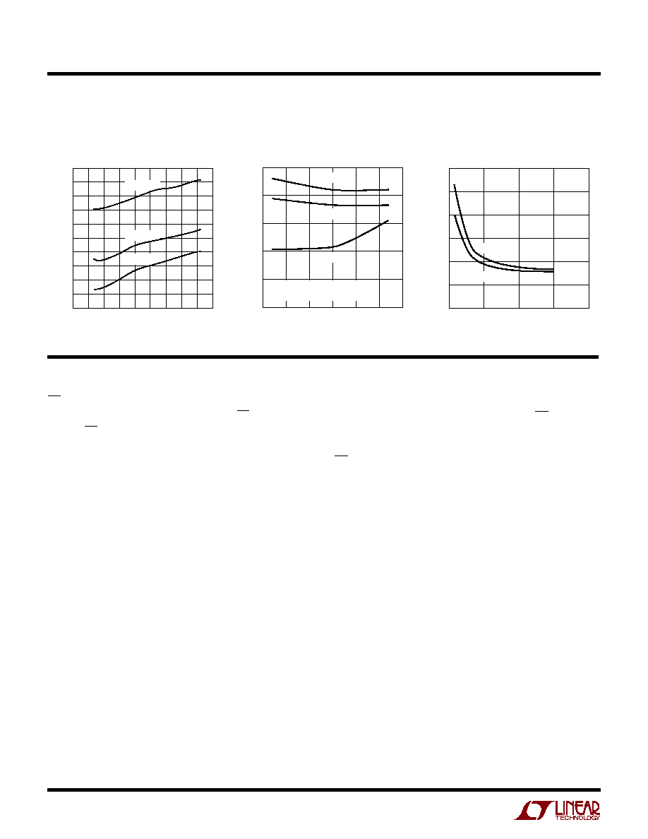
TYPICAL PERFOR A CE CHARACTERISTICS
U
W
I
CC
vs Temperature
Input Output High to Low
Propagation Delay vs
Temperature
Connection Circuitry V
OUT
V
IN
50
25
0
25
50
75
100
TEMPERATURE (
°
C)
TIME (ns)
4301 G02
100
80
60
40
20
0
V
CC
= 2.7V
V
CC
= 3.3V
V
CC
= 5.5V
C
IN
= C
OUT
= 100pF
R
PULLUPIN
= R
PULLUPOUT
= 10k
R
PULLUP
(
)
0
10,000
20,000
30,000
40,000
V
OUT
V
IN
(mV)
4301 G03
300
250
200
150
100
50
0
V
CC
= 3.3V
V
CC
= 5V
T
A
= 25
°
C
V
IN
= 0V
TEMPERATURE (
°
C)
80
I
CC
(mA)
4.9
4.8
4.7
4.6
4.5
4.4
4.3
4.2
4.1
4.0
3.9
40
0
20
100
4301 G01
60
20
40
60
80
V
CC
= 5.5V
V
CC
= 3.3V
V
CC
= 2.7V
5
LTC4301L
4301lf
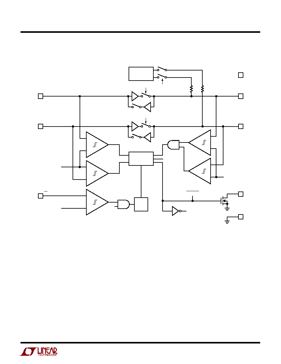
BLOCK DIAGRA
W
CONNECT PRECHARGE
CONNECT
CONNECT
1
R1
200k
R2
200k
PRECHARGE
LOGIC
PRECHARGE
CONNECT
95
µ
s
DELAY
UVLO
1.4V
CS
0.6V
3
SCLIN
6
SDAIN
1.8V
CONNECT
CONNECT
7
SDAOUT
8
V
CC
2
SCLOUT
READY
5
GND
4301l BD
4
LTC4301L Supply Independent 2-Wire Bus Buffer