 | ÐлекÑÑоннÑй компоненÑ: LTC4302 | СкаÑаÑÑ:  PDF PDF  ZIP ZIP |
4302f.pm6
LTC4302-1/LTC4302-2
1
sn430212 430212fs
APPLICATIO S
U
FEATURES
TYPICAL APPLICATIO
U
DESCRIPTIO
U
The LTC
®
4302-1/LTC4302-2 addressable I
2
C bus and
SMBus compatible bus buffers allow a peripheral board
to be inserted and removed from a live backplane without
corruption of the bus. The LTC4302-1/LTC4302-2 main-
tain electrical isolation between the backplane and periph-
eral board until their V
CC
supply is valid and a master
device on the backplane side addresses the LTC4302-1/
LTC4302-2 and commands them to connect. The
LTC4302-1/LTC4302-2's ADDRESS pin provides 32 pos-
sible addresses set by an external resistive divider be-
tween V
CC
and GND. The LTC4302-1/LTC4302-2 work
with supply voltages ranging from 2.7V to 5.5V. The SDA
and SCL inputs and outputs do not load the bus lines when
V
CC
is low.
Rise time accelerator circuitry* allows for heavier capaci-
tive bus loading while still meeting system timing require-
ments. During insertion, the SDA and SCL lines are
precharged to 1V to minimize bus disturbances. Two
general purpose input/output pins (GPIOs) on the
LTC4302-1 can be configured as inputs, open-drain out-
puts or push-pull outputs. The LTC4302-2 option replaces
one GPIO pin with a second supply voltage pin V
CC2
,
providing level shifting between systems with different
supply voltages. The LTC4302-1/LTC4302-2 are available
in a 10-pin MSOP package.
s
Live Board Insertion
s
5V/3.3V Level Translator
s
Servers
s
Capacitance Buffer/Bus Extender
s
Nested Addressing
, LTC and LT are registered trademarks of Linear Technology Corporation.
s
Bidirectional Buffer for SDA and SCL Lines
Increases Fanout
s
Connect SDA and SCL Lines with 2-Wire Bus
Commands
s
Prevents SDA and SCL Corruption During Live Board
Insertion and Removal from Backplane
s
Compatible with I
2
C
TM
Standard Mode, I
2
C Fast
Mode and SMBus Standards
s
Rise Time Accelerators on SDA, SCL Lines
s
1V Precharge on SDA and SCL Lines
s
32 Unique Addresses from a Single ADDRESS Pin
s
Two General Purpose Inputs-Outputs (LTC4302-1)
s
Translates Between 5V and 3.3V Systems
(LTC4302-2)
s
Small 10-Pin MSOP Package
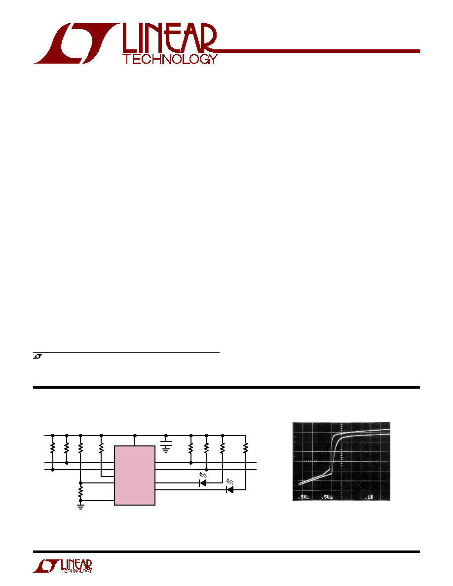
Addressable
2-Wire Bus Buffers
V
CC
LTC4302-1
SDAIN
C1
0.01
µ
F
CARD SDA
CARD SCL
R7
10k
R6
10k
R8
1k
R9
1k
2.7V
to
5.5V
R3
10k
R4
10k
R5
10k
R1
1870
R2
2000
SDA
SCL
SCLIN
CONN
ADDRESS
GND
LED
LED
4203 TA01a
SDAOUT
SCLOUT
GPIO1
GPIO2
I
2
C is a trademark of Philips Electronics N.V.
*U.S. Patent No. 6,650,174
4032 F10
OUTPUT
SIDE
50pF
INPUT
SIDE
150pF
Input-Output Connection t
PLH
0.1
µ
s/DIV
LTC4302-1/LTC4302-2
2
sn430212 430212fs
SYMBOL
PARAMETER
CONDITIONS
MIN
TYP
MAX
UNITS
Power Supply/Start-Up
V
CC
Positive Supply Voltage
LTC4302-1
q
2.7
5.5
V
V
CC2
Card Side Supply Voltage
LTC4302-2
q
2.7
5.5
V
I
CC
Supply Current
V
SDAIN
= 0V, V
CC
= 5.5V (Note 2) LTC4302-1
q
5.9
8
mA
I
VCC
V
CC
Supply Current
V
SDAIN
= 0V, V
CC
= V
CC2
= 5.5V
q
3.4
5
mA
(Note 2) LTC4302-2
I
VCC2
V
CC2
Supply Current
V
SDAIN
= 0V, V
CC
= V
CC2
= 5.5V
q
2.3
4
mA
(Note 2) LTC4302-2
V
UVLOU
UVLO Upper Threshold
V
CC
Rising
q
2.5
2.7
V
V
UVLOL
UVLO Lower Threshold
V
CC
Falling
2.35
V
V
UVLO2U
V
CC2
UVLO Upper Threshold
LTC4302-2
q
2.5
2.7
V
V
UVLO2L
V
CC2
UVLO Lower Threshold
LTC4302-2
2.35
V
V
PRE
Precharge Voltage
SDA, SCL Floating
q
0.8
1
1.2
V
V
THCONN
CONN Threshold Voltage
q
0.8
1.5
2.2
V
t
PHL
CONN Delay, On-Off
60
ns
t
PLH
CONN Delay, Off-On
20
ns
V
CC
to GND ................................................. 0.3V to 7V
SDAIN, SCLIN, SDAOUT, SCLOUT,
GPIO1, CONN, GPIO2 (LTC4302-1),
V
CC2
(LTC4302-2) ........................................ 0.3V to 7V
ADDRESS ....................................... 0.3V to V
CC
+ 0.3V
ORDER PART
NUMBER
Consult LTC Marketing for parts specified with wider operating temperature ranges.
LTC4302CMS-1
LTC4302IMS-1
(Note 1)
T
JMAX
= 125
°
C,
JA
= 130
°
C/W
MS PART MARKING
LTYF
LTYG
ABSOLUTE AXI U RATI GS
W
W
W
U
PACKAGE/ORDER I FOR ATIO
U
U
W
Operating Temperature Range
LTC4302C-1/LTC4302C-2 ...................... 0
°
C to 70
°
C
LTC4302I-1/LTC4302I-2 .................... 40
°
C to 85
°
C
Storage Temperature Range ................. 65
°
C to 125
°
C
Lead Temperature (Soldering, 10 sec).................. 300
°
C
ORDER PART
NUMBER
MS PART MARKING
1
2
3
4
5
SDAIN
SCLIN
CONN
ADDRESS
GND
10
9
8
7
6
SDAOUT
SCLOUT
V
CC
GPIO2
GPIO1
TOP VIEW
MS PACKAGE
10-LEAD PLASTIC MSOP
LTC4302CMS-2
LTC4302IMS-2
LTABY
LTABZ
ELECTRICAL CHARACTERISTICS
The
q
denotes the specifications which apply over the full operating temperature range, otherwise specifications are at T
A
= 25
°
C.
V
CC
= 2.7V to 5.5V (LTC4302-1), V
CC
= V
CC2
= 2.7V to 5.5V (LTC4302-2) unless otherwise noted.
T
JMAX
= 125
°
C,
JA
= 130
°
C/W
1
2
3
4
5
SDAIN
SCLIN
CONN
ADDRESS
GND
10
9
8
7
6
SDAOUT
SCLOUT
V
CC
V
CC2
GPIO1
TOP VIEW
MS PACKAGE
10-LEAD PLASTIC MSOP
LTC4302-1/LTC4302-2
3
sn430212 430212fs
ELECTRICAL CHARACTERISTICS
The
q
denotes the specifications which apply over the full operating temperature range, otherwise specifications are at T
A
= 25
°
C.
V
CC
= 2.7V to 5.5V (LTC4302-1), V
CC
= V
CC2
= 2.7V to 5.5V (LTC4302-2) unless otherwise noted.
Note 1: Absolute Maximum Ratings are those values beyond which the life
of a device may be impaired.
Note 2: The I
CC
tests are performed with the backplane-to-card connection
circuitry activated.
Note 3: When the GPIOs are in open-drain output or input mode, the logic
high voltage can be provided by a pull-up supply voltage ranging from
2.2V to 5.5V, independent of the V
CC
voltage.
Note 4: I
PULLUP,AC
varies with temperature and V
CC
voltage as shown in
the Typical Performance Characteristics section.
Note 5: The connection circuitry always regulates its output to a higher
voltage than its input. The magnitude of this offset voltage as a function of
the pull-up resistor and V
CC
voltage is shown in the Typical Performance
Characteristics section.
Note 6: The specifications in this section illustrate the LTC4302-1/
LTC4302-2's compatibility with the I
2
C Fast Mode, the I
2
C Standard Mode
and SMBus specifications. See the Timing Diagram on page 5 for
illustrations of the timing parameters.
Note 7: C
B
= total capacitance of one bus line in pF.
Note 8: The digital interface circuit controls the data fall time only when
acknowledging or transmitting zeros during a read operation. The input-
output connection data and clock outputs meet the fall time specification
provided that the corresponding inputs meet the fall time specification.
Note 9: Guaranteed by design. Not subject to test.
SYMBOL
PARAMETER
CONDITIONS
MIN
TYP
MAX
UNITS
General Purpose I/Os
V
LOW
I/O Logic Low Voltage
I
SINK
= 10mA, V
CC
= 2.7V
q
0.36
0.8
V
V
HIGH
I/O Logic High Voltage
I
SOURCE
= 200
µ
A, V
CC
= 2.7V
q
2.4
V
I
LEAK
I/O Leakage Current
V
I/O
= 0V to 5.5V (Note 3)
q
±
5
µ
A
V
THRESH
Input Threshold Voltage
Input Mode
q
0.8
1.5
2.2
V
Rise Time Accelerators
I
PULLUP,AC
Transient Boosted Pull-Up Current
Positive Transition on SDA, SCL,
q
1
2
mA
Slew Rate = 0.8V/
µ
s, V
CC
= 2.7V (Note 4)
Input-Output Connection
V
OS
Output-Input Offset Voltage
10k to V
CC
on SDA, SCL Pins (Note 5),
q
0
100
175
mV
C
IN
Digital Input Capacitance
(Note 9)
10
pF
V
OL
Output Low Voltage
SDA, SCL Pins, I
SINK
= 3mA
q
0
0.4
V
I
LEAK
Input Leakage Current
SDA, SCL Pins, V
CC
= 0V to 5.5V
q
±
5
µ
A
Connection Circuits Inactive
2-Wire Digital Interface Voltage Characteristics
V
LTH
Logic Threshold Voltage
q
0.3V
CC
0.5V
CC
0.7V
CC
V
I
LEAK
Digital Input Leakage
V
CC
= 0V to 5.5V
q
±
5
µ
A
V
OL
Digital Output Low Voltage
I
PULLUP
= 3mA Into SDAIN Pin
q
0.4
V
2-Wire Digital Interface Timing Characteristics (Note 6)
f
I2C,MAX
I
2
C Operating Frequency
(Note 9)
400
600
kHz
t
BUF
Bus Free Time Between Stop and Start
(Note 9)
0.75
1.3
µ
s
Condition
t
HD,STA
Hold Time After (Repeated) Start Condition
(Note 9)
45
100
ns
t
SU,STA
Repeated Start Condition Setup Time
(Note 9)
30
0
ns
t
SU,STO
Stop Condition Setup Time
(Note 9)
30
0
ns
t
HD,DATI
Data Hold Time Input
(Note 9)
25
0
ns
t
HD,DATO
Data Hold Time Output
300
600
900
ns
t
SU,DAT
Data Setup Time
(Note 9)
50
100
ns
t
SP
Pulse Width of Spikes Suppressed by
(Note 9)
50
150
250
ns
the Input Filter
t
f
Data Fall Time
(Notes 7, 8, 9)
20 +
300
ns
0.1C
B
LTC4302-1/LTC4302-2
4
sn430212 430212fs
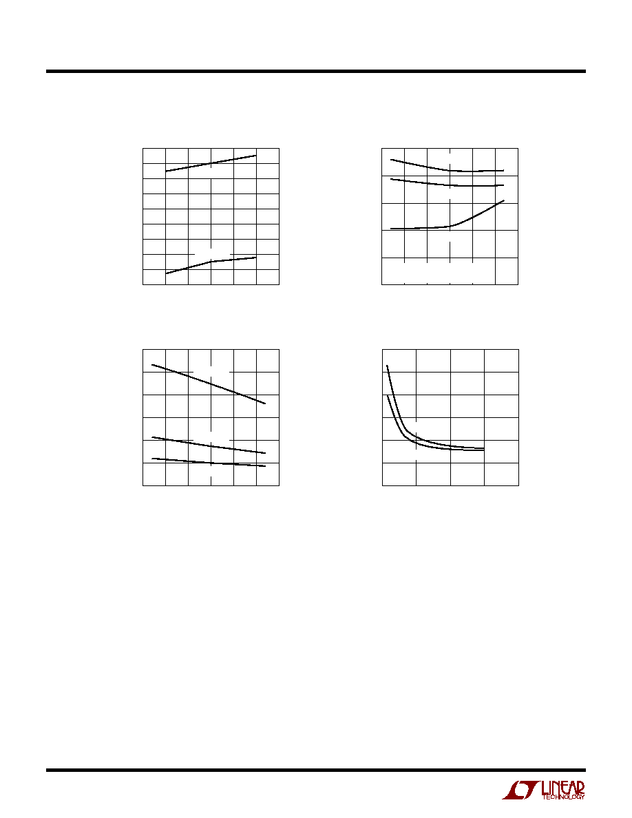
TYPICAL PERFOR A CE CHARACTERISTICS
U
W
40
25
85
TEMPERATURE (
°
C)
I
CC
(mA)
4302 G01
6.1
5.9
5.7
5.5
5.3
5.1
4.9
4.7
4.5
4.3
V
CC
= 5.5V
V
CC
= 2.7V
50
25
0
25
50
75
100
TEMPERATURE (
°
C)
t
PHL
(ns)
4302 G02
100
80
60
40
20
0
V
CC
= 2.7V
V
CC
= 3.3V
V
CC
= 5.5V
C
IN
= C
OUT
= 100pF
R
PULLUPIN
= R
PULLUPOUT
= 10k
I
CC
vs Temperature
Input Output t
PHL
vs Temperature
I
PULLUPAC
vs Temperature
SDA, SCL V
OS
50
25
0
25
50
75
100
TEMPERATURE (
°
C)
I
PULLUPAC
(mA)
4302 G03
12
10
8
6
4
2
0
V
CC
= 2.7V
V
CC
= 5V
V
CC
= 3V
R
PULLUP
(K
)
0
10
20
30
40
V
OUT
V
IN
(mV)
4302 G04
300
250
200
150
100
50
0
V
CC
= 3.3V
V
CC
= 5V
V
IN
= 0V
(Specifications are at T
A
= 25
°
C unless otherwise noted.)
LTC4302-1/LTC4302-2
5
sn430212 430212fs
U
U
U
PI FU CTIO S
SDAIN (Pin 1): Serial Data Input. Connect this pin to the
SDA bus on the backplane. Do not float.
SCLIN (Pin 2): Serial Clock Input. Connect this pin to the
SCL bus on the backplane. Do not float.
CONN (Pin 3): Register Reset and Connection Sense
Input. Driving this pin low resets the registers to their
default state: GPIOs in output open-drain high impedance
mode, rise time accelerators disabled and the input-to-
output connection disabled. Communication with the
LTC4302-1/LTC4302-2 is disabled when CONN is low.
When CONN is brought back high, the registers remain in
the default state and communication is enabled.
ADDRESS (Pin 4): 2-Wire Address Programming Input.
The 2-wire address is programmed by connecting
ADDRESS to a resistive divider between V
CC
and ground.
The voltage on ADDRESS is converted by an internal
analog-to-digital (A/D) converter into a 5-bit digital word.
This resulting digital code represents the least significant
five bits of the 2-wire address. 1% resistors must be used
to ensure accurate address programming. 32 unique
addresses are possible. See Table 1 for 1% resistor values
and corresponding addresses. Care must also be taken to
minimize capacitance on ADDRESS. Resistors must be
placed close to the LTC4302-1/LTC4302-2's V
CC
, GND
and ADDRESS pins.
GND (Pin 5): Ground. Connect this pin to a ground plane
for best results.
GPIO1 (Pin 6): General Purpose Input/Output (GPIO1).
GPIO1 can be used as an input, an open-drain output or a
push-pull output. The N-Channel MOSFET pulldown de-
vice is capable of driving LEDs. When used in input or
open-drain output mode, the I/O pin can be pulled up to a
supply voltage ranging from 2.2V to 5.5V independent of
the V
CC
voltage.
GPIO2 (Pin 7, LTC4302-1): General Purpose Input/Out-
put. GPIO2 can be used as an input, an open-drain output,
or a push-pull output. The N-Channel MOSFET pulldown
device is capable of driving LED's. When used in input or
open-drain output mode, the I/O pin can be pulled up to a
supply voltage ranging from 2.2V to 5.5V independent of
the V
CC
voltage.
V
CC2
(Pin 7, LTC4302-2): Card Side Supply Voltage. This
pin is a power supply pin for the card side busses. Connect
V
CC2
to the card's V
CC
and connect a bypass capacitor of
at least 0.01
µ
F directly between V
CC2
and GND for best
results.
V
CC
(Pin 8): Main Input Power Supply from Backplane.
Connect a bypass capacitor of at least 0.01
µ
F directly
between V
CC
and GND for best results.
SCLOUT (Pin 9): Serial Clock Output. Connect this pin to
the SCL bus on the I/O card. Do not float.
SDAOUT (Pin 10): Serial Data Output. Connect this pin to
the SDA bus on the I/O card. Do not float.
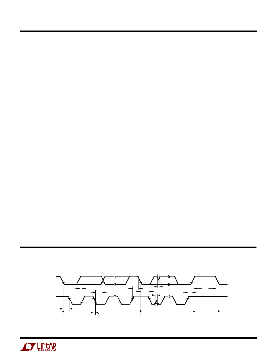
t
SU, DAT
t
SU, STO
t
SU, STA
t
BUF
t
HD, STA
t
SP
t
SP
t
HD, DATO,
t
HD, DATI
t
HD, STA
t
f
START
CONDITION
STOP
CONDITION
REPEATED START
CONDITION
START
CONDITION
4302 TD01
SDA
SCL
TI I G DIAGRA
U
W
W