 | ÐлекÑÑоннÑй компоненÑ: LTC4305 | СкаÑаÑÑ:  PDF PDF  ZIP ZIP |
4305.pm6
LTC4305
1
4305f
APPLICATIO S
U
TYPICAL APPLICATIO
U
FEATURES
DESCRIPTIO
U
The LTC
®
4305 is a 2-channel, 2-wire bus multiplexer with
bus buffers to provide capacitive isolation between the
upstream bus and downstream buses. Through software
control, the LTC4305 connects the upstream 2-wire bus
to any desired combination of downstream channels.
Each channel can be pulled up to a supply voltage ranging
from 2.2V to 5.5V, independent of the LTC4305 supply
voltage. The downstream channels are also provided with
an ALERT1ALERT2 inputs for fault reporting.
Programmable timeout circuitry disconnects the down-
stream buses if the bus is stuck low. When activated, rise
time accelerators source currents into the 2-wire bus pins
to reduce rise time. Driving the ENABLE pin low restores
all features to their default states. Three address pins
provide 27 distinct addresses.
The LTC4305 is available in 16-lead (4mm
× 5mm) DFN
and SSOP packages.
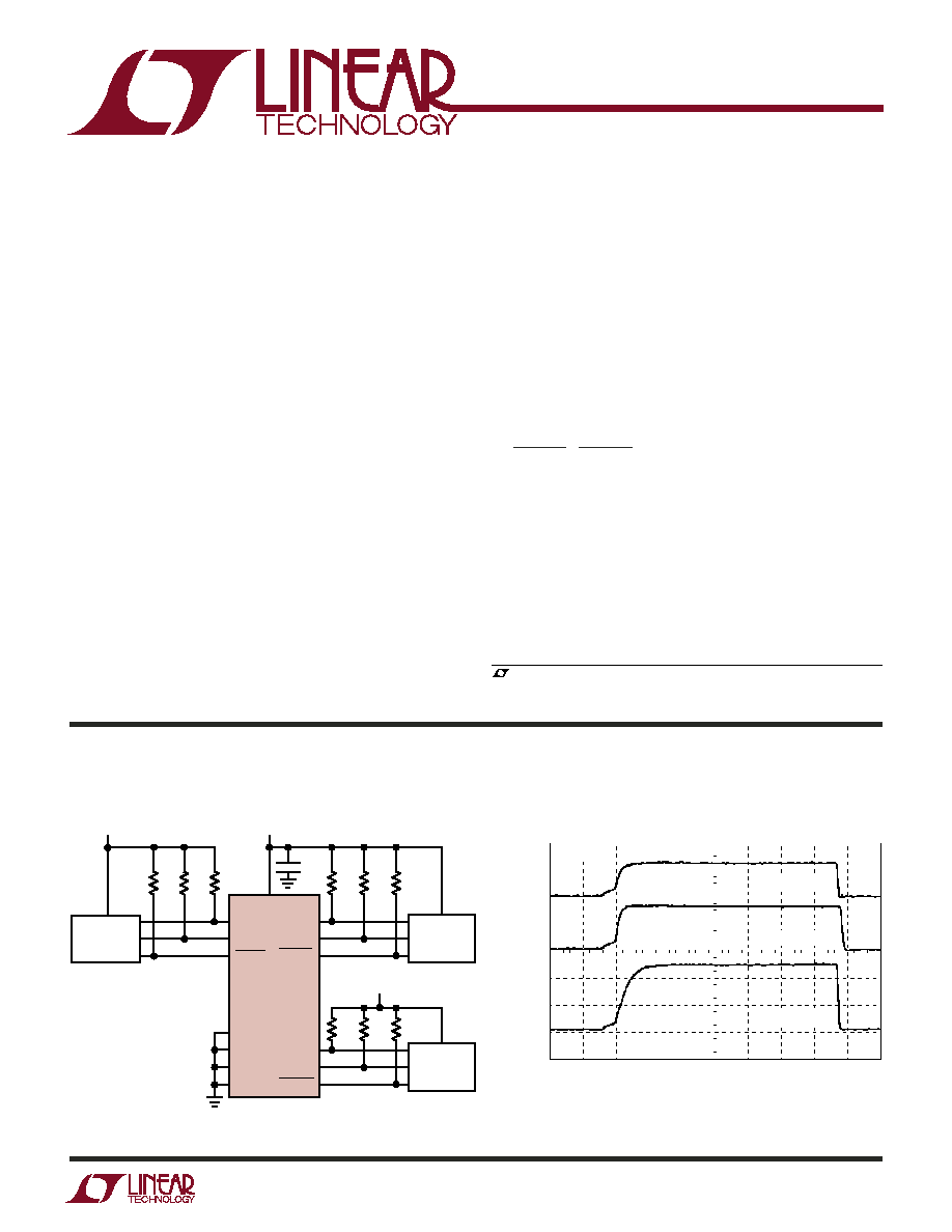
Nested Addressing
5V/3.3V Level Translator
Capacitance Buffer/Bus Extender
1:2 2-Wire Multiplexer/Switch
Connect SDA and SCL Lines with 2-Wire Bus
Commands
Supply Independent Bidirectional Buffer for SDA
and SCL Lines Increases Fan-Out
Programmable Disconnect from Stuck Bus
Compatible with I
2
C and SMBus Standards
Rise Time Accelerator Circuitry
SMBus Compatible ALERT Response Protocol
Prevents SDA and SCL Corruption During Live Board
Insertion and Removal from Backplane
±10kV Human Body Model ESD Ruggedness
16-Lead (4mm
× 5mm) DFN and SSOP Packages
2-Channel,
2-Wire Bus Multiplexer with
Capacitance Buffering
, LTC and LT are registered trademarks of Linear Technology Corporation. All other
trademarks are the property of their respective owners. Patent Pending.
A Level-Shifting and Nested Addressing Application
10k
0.01
µF
10k
10k
10k
10k
10k
ADDRESS = 1000 100
SFP
MODULE #1
10k
10k
10k
ADDRESS = 1111 000
MICRO-
CONTROLLER
SFP
MODULE #2
ADDRESS = 1111 000
2.5V
5V
3.3V
4305 TA01
SCLIN
SDAIN
ALERT
ADR2
ADR1
ADR0
GND
SCL1
SDA1
ALERT1
SCL2
SDA2
ALERT2
V
CC
LTC4305
4305 TA01b
V
CC
= 3.3V
VCARD1 = 3.3V
VCARD2 = 5V
VBACK = 2.5V
SCL2
2V/DIV
500ns/DIV
SCL1
2V/DIV
SCLIN
2V/DIV
I
2
C Bus Waveforms
LTC4305
4305f
2
ABSOLUTE AXI U
RATI GS
W
W
W
U
(Note 1)
Supply Voltage (V
CC
) ................................... 0.3V to 7V
Input Voltages (ADR0, ADR1, ADR2,
ENABLE, ALERT1, ALERT2) .................... 0.3V to 7V
Output Voltages (ALERT, READY) ............... 0.3V to 7V
Input/Output Voltages (SDAIN, SCLIN,
SCL1, SDA1, SCL2, SDA2) ...................... 0.3V to 7V
Output Sink Current (SDAIN, SCLIN, SCL1,
SDA1, SCL2, SDA2, ALERT, READY) ............... 10mA
Operating Temperature Range
LTC4305C ............................................... 0
°C to 70°C
LTC4305I ............................................. 40
°C to 85°C
Storage Temperature Range
DHD Package .................................... 65
°C to 125°C
GN Package ....................................... 65
°C to 150°C
Lead Temperature (Soldering, 10 sec)
GN Package ...................................................... 300
°C
ELECTRICAL CHARACTERISTICS
The
denotes specifications which apply over the full specified temperature
range, otherwise specifications are at T
A
= 25
°C. V
CC
= 3.3V unless otherwise noted.
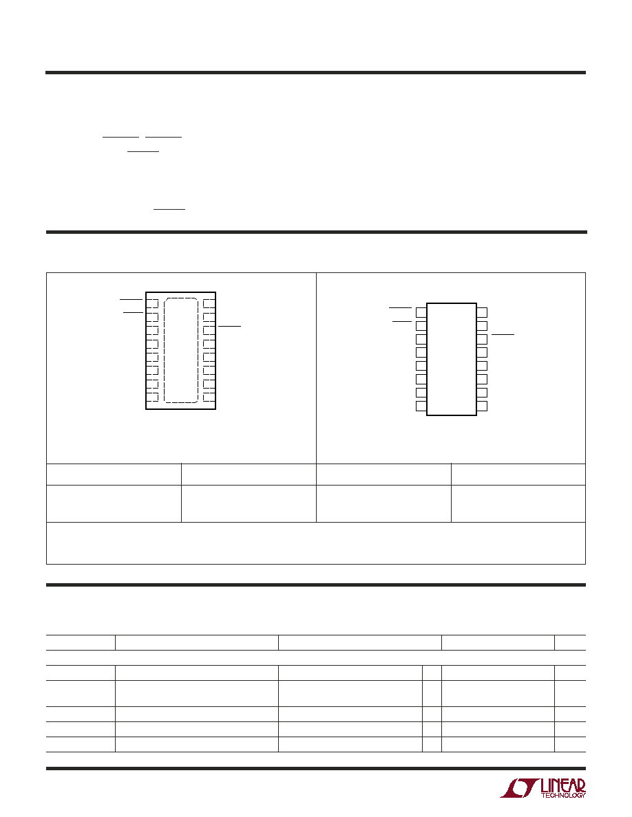
PACKAGE/ORDER I FOR ATIO
U
U
W
Consult LTC Marketing for parts specified with wider operating temperature ranges.
GN PART MARKING
4305
4305I
Order Options Tape and Reel: Add #TR
Lead Free: Add #PBF Lead Free Tape and Reel: Add #TRPBF
Lead Free Part Marketing:
http://www.linear.com/leadfree/
T
JMAX
= 125
°C,
JA
= 135
°C/W
1
2
3
4
5
6
7
8
TOP VIEW
GN PACKAGE
16-LEAD NARROW PLASTIC SSOP
16
15
14
13
12
11
10
9
ALERT2
ALERT
SDAIN
GND
SCLIN
ENABLE
V
CC
ADR0
SCL2
SDA2
ALERT1
SDA1
SCL1
READY
ADR2
ADR1
16
15
14
13
12
11
10
9
17
1
2
3
4
5
6
7
8
SCL2
SDA2
ALERT1
SDA1
SCL1
READY
ADR2
ADR1
ALERT2
ALERT
SDAIN
GND
SCLIN
ENABLE
V
CC
ADRO
TOP VIEW
DHD PACKAGE
16-LEAD (4mm
× 5mm) PLASTIC DFN
EXPOSED PAD (PIN 17) PCB CONNECTION OPTIONAL
MUST BE CONNECTED TO PCB TO OBTAIN
JA
= 43
°C/W OTHERWISE
JA
= 140
°C/W. T
JMAX
= 125
°C
LTC4305CDHD
LTC4305IDHD
ORDER PART NUMBER
DHD PART MARKING
4305
4305
LTC4305CGN
LTC4305IGN
ORDER PART NUMBER
SYMBOL
PARAMETER
CONDITIONS
MIN
TYP
MAX
UNITS
Power Supply/Start-Up
V
CC
Input Supply Range
2.7
5.5
V
I
CC
Input Supply Current
Downstream Connected, V
CC
= 5.5V
5.2
8
mA
SCL Bus Low, SDA Bus High
I
CC ENABLE
=
0V
Input Supply Current
V
ENABLE
= 0V, V
CC
= 5.5V
1.25
2.5
mA
V
UVLOU
UVLO Upper Threshold Voltage
2.3
2.5
2.7
V
V
UVLOHYST
UVLO Threshold Hysteresis Voltage
100
175
250
mV
LTC4305
3
4305f
ELECTRICAL CHARACTERISTICS
The
denotes specifications which apply over the full specified temperature
range, otherwise specifications are at T
A
= 25
°C. V
CC
= 3.3V unless otherwise noted.
SYMBOL
PARAMETER
CONDITIONS
MIN
TYP
MAX
UNITS
Power Supply/Start-Up
V
TH EN
ENABLE Falling Threshold Voltage
0.8
1.0
1.2
V
V
EN HYST
ENABLE Threshold Hysteresis Voltage
60
mV
t
PHL EN
ENABLE Delay, On-Off
60
ns
t
PLH EN
ENABLE Delay, Off-On
20
ns
I
IN
EN
ENABLE Input Leakage Current
V
ENABLE
= 0V, 5.5V, V
CC
= 5.5V
0.1
±
1
µA
V
LOW READY
READY Pin Logic Low Output Voltage
I
PULL-UP
= 3mA, V
CC
= 2.7V
0.18
0.4
V
I
OFF READY
READY Off State Input Leakage Current
V
READY
= 0V, 5.5V, V
CC
= 5.5V
0
±
1
µA
ALERT
V
ALERT(OL)
ALERT Output Low Voltage
I
ALERT
= 3mA, V
CC
= 2.7V
0.2
0.4
V
I
OFF,
ALERT
ALERT Off State Input Leakage Current
V
ALERT
= 0V, 5.5V
0
±
1
µA
I
IN,
ALERT12
ALERT1ALERT2 Input Current
V
ALERT12
= 0V, 5.5V
0
±
1
µA
V
ALERT12(IN)
ALERT1ALERT2 Pin Input Falling
0.8
1.0
1.2
V
Threshold Voltages
V
ALERT12(HY)
ALERT1ALERT2 Pin Input Threshold
80
mV
Hysteresis Voltages
Rise Time Accelerators
V
SDA,SCL slew
Initial Slew Requirement to Activate
SDAIN, SCLIN, SDA12,
0.4
0.8
V/
µs
Rise Time Accelerator Currents
SCL12 Pins
V
RISE,DC
Rise Time Accelerator DC Threshold Voltage
SDAIN, SCLIN, SDA12,
0.7
0.8
1
V
SCL12 Pins
I
BOOST
Rise Time Accelerator Pull-Up Current
SDAIN, SCLIN, SDA12,
4
5.5
mA
SCL12 Pins (Note 3)
Stuck Low Timeout Circuitry
V
TIMER(L)
Stuck Low Falling Threshold Voltage
V
CC
= 2.7V, 5.5V
0.4
0.52
0.64
V
V
TIMER(HYST)
Stuck Low Threshold Hysteresis Voltage
80
mV
T
TIMER1
Timeout Time #1
TIMSET1,0 = 01
25
30
35
ms
T
TIMER2
Timeout Time #2
TIMSET1,0 = 10
12.5
15
17.5
ms
T
TIMER3
Timeout Time #3
TIMSET1,0 = 11
6.25
7.5
8.75
ms
Upstream-Downstream Buffers
V
OS,BUF
Buffer Offset Voltage
R
BUS
= 10k, V
CC
= 2.7V, 5.5V (Note 4)
25
60
100
mV
V
OS,UP-BUF
Upstream Buffer Offset Voltage
V
CC
= 2.7V, R
BUS
= 2.7k (Note 4)
40
80
120
mV
V
IN,BUFFER
= 0V
V
CC
= 5.5V, R
BUS
= 2.7k (Note 4)
70
110
150
mV
V
OS,DOWN-BUF
Downstream Buffer Offset Voltage
V
CC
= 2.7V, R
BUS
= 2.7k (Note 4)
60
110
160
mV
V
IN,BUFFER
= 0V
V
CC
= 5.5V, R
BUS
= 2.7k (Note 4)
80
140
200
mV
V
OL
Output Low Voltage, V
IN,BUFFER
= 0V
SDA, SCL Pins; I
SINK
= 4mA,
400
mV
V
CC
= 3V, 5.5V
V
OL
Output Low Voltage, V
IN,BUFFER
= 0.2V
SDA, SCL Pins; I
SINK
= 500
µA,
320
mV
V
CC
= 2.7V, 5.5V
V
IL,MAX
Buffer Input Logic Low Voltage
V
CC
= 2.7V, 5.5V
0.4
0.52
0.64
V
V
THSDA,SCL
Downstream SDA, SCL Logic Threshold Voltage
0.8
1.0
1.2
V
I
LEAK
Input Leakage Current
SDA, SCL Pins;
±5
µA
V
CC
= 0 to 5.5V;
Buffers Inactive
LTC4305
4305f
4
The
denotes specifications which apply over the full specified temperature
range, otherwise specifications are at T
A
= 25
°C. V
CC
= 3.3V unless otherwise noted.
ELECTRICAL CHARACTERISTICS
Note 1: Absolute Maximum Ratings are those values beyond which the life
of a device may be impaired.
Note 2: Guaranteed by design and not subject to test, unless stated
otherwise in the Conditions.
Note 3: The boosted pull-up currents are regulated to prevent excessively
fast edges for light loads. See the Typical Performance Characteristics for
rise time as a function of V
CC
and parasitic bus capacitance C
BUS
and for
I
BOOST
as a function of V
CC
and temperature.
Note 4: When a logic low voltage V
LOW
is forced on one side of the
upstream-downstream buffers, the voltage on the other side is regulated
to a voltage V
LOW2
= V
LOW
+ V
OS
is a positive offset voltage. V
OS,DOWN-BUF
is the offset voltage when the LTC4305 is driving the upstream pin (e.g.,
SDAIN) and V
OS,DOWN-BUF
is the offset voltage when the LTC4305 is
driving the downstream pin (e.g., SDA1). See the Typical Performance
Characteristics for V
OS,UP-BUF
and V
OS,DOWN-BUF
as a function of V
CC
and
bus pull-up current.
Note 5: When floating, the ADR0ADR2 pins can tolerate pin leakage
currents up to I
ADR,FLOAT
and still convert the address correctly.
SYMBOL
PARAMETER
CONDITIONS
MIN
TYP
MAX
UNITS
I
2
C Interface
V
ADR(H)
ADR02 Input High Voltage
0.75
· V
CC
0.9
· V
CC
V
V
ADR(L)
ADR02 Input Low Voltage
0.1
· V
CC
0.25
· V
CC
V
I
ADR(IN, L)
ADR02 Logic Low Input Current
ADR02 = 0V, V
CC
= 5.5V
30
60
80
µA
I
ADR(IN, H)
ADR02 Logic High Input Current
ADR02 = V
CC
= 5.5V
30
60
80
µA
I
ADR,FLOAT
ADR02 Allowed Input Current
V
CC
= 2.7V, 5.5V (Note 5)
±5
±13
µA
V
SDAIN,SCLIN(TH)
SDAIN, SCLIN Input Falling Threshold Voltages
V
CC
= 5.5V
1.4
1.6
1.8
V
V
SDAIN,SCLIN(HY)
SDAIN, SCLIN Hysteresis
30
mV
I
SDAIN,SCLIN(OH)
SDAIN, SCLIN Input Current
SCL, SDA = V
CC
±
5
µA
C
IN
SDA, SCL Input Capacitance
(Note 2)
6
10
pF
V
SDAIN(OL)
SDAIN Output Low Voltage
I
SDA
= 4mA, V
CC
= 2.7V
0.2
0.4
V
I
2
C Interface Timing
f
SCL
Maximum SCL Clock Frequency
(Note 2)
400
kHz
t
BUF
Bus Free Time Between Stop/Start Condition
(Note 2)
0.75
1.3
µs
t
HD, STA
Hold Time After (Repeated) Start Condition
(Note 2)
45
100
ns
t
SU, STA
Repeated Start Condition Set-Up Time
(Note 2)
30
0
ns
t
SU, STO
Stop Condition Set-Up Time
(Note 2)
30
0
ns
t
HD, DATI
Data Hold Time Input
(Note 2)
25
0
ns
t
HD, DATO
Data Hold Time Output
(Note 2)
300
600
900
ns
t
SU, DAT
Data Set-Up Time
(Note 2)
50
100
ns
t
f
SCL, SDA Fall Times
(Note 2)
20 + 0.1
·
300
ns
C
BUS
t
SP
Pulse Width of Spikes Suppressed by the
(Note 2)
50
150
250
ns
Input Filter
LTC4305
5
4305f
CAPACITANCE, C
BUS
(pF)
0
RISE TIME (ns)
150
200
250
800
4305 G02
100
50
0
200
400
600
1000
V
CC
= 3.3V
V
CC
= 5V
dV = 0.3V · V
CC
TO 0.7V · V
CC
R
BUS
= 10k
TEMPERATURE (
°C)
50
t
PHL
(ns)
80
100
120
25
75
4305 G01
60
40
25
0
50
100
125
20
0
V
CC
= 3.3V
V
CC
= 5V
TEMPERATURE (
°C)
50
CURRENT (mA)
4
5
6
25
75
4305 G03
3
2
25
0
50
100
125
1
0
V
CC
= 3.3V
V
CC
= 5V
UPSTREAM CONNECTED TO CHANNEL 1,
SCL BUS LOW, SDA BUS HIGH
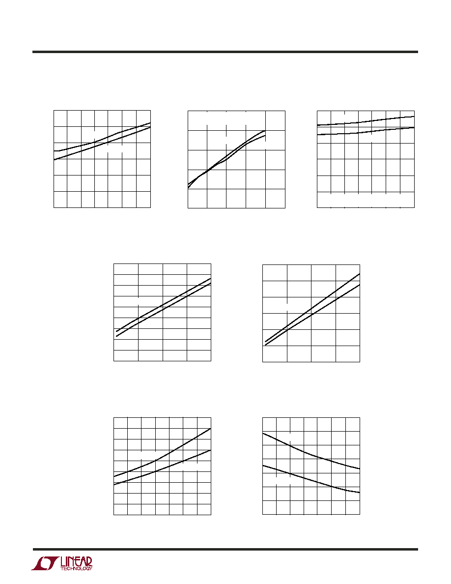
TYPICAL PERFOR A CE CHARACTERISTICS
U
W
Rise Time vs C
BUS
vs V
CC
Buffer Circuitry t
PHL
vs Temperature
I
CC
vs Temperature
V
OS,DOWN-BUF
vs Bus Pull-Up Current
V
OS,UP-BUF
vs Bus Pull-Up Current
I
BOOST
vs Temperature
BUS PULL-UP CURRENT (mA)
1
0
V
OS
(mV)
100
120
140
4305 G04
80
60
0
2
3
4
40
20
180
160
V
CC
= 3.3V
V
CC
= 5V
BUS PULL-UP CURRENT (mA)
0
0
V
OS
(mV)
50
100
150
200
250
300
1
2
3
4
4305 G05
V
CC
= 3.3V
V
CC
= 5V
(T
A
= 25
°C unless otherwise specified.)
Downstream R
FET
on Resistance
vs V
CC
and Temperature
TEMPERATURE (
°C)
50
0
R
ON
(
)
5
15
20
25
50
45
4305 G06
10
0
25
75
100
25
125
30
35
40
V
CC
= 3.3V
V
CC
= 5V
TEMPERATURE (
°C)
50
25
75
25
0
50
100
125
I
BOOST
(mA)
10
12
4305 G07
8
6
0
4
2
14
V
CC
= 3.3V
V
CC
= 5V