Äîêóìåíòàöèÿ è îïèñàíèÿ www.docs.chipfind.ru
1
LTC4350
4350fa
Hot Swappable
Load Share Controller
The LTC
®
4350 is a load share controller that allows
systems to equally load multiple power supplies con-
nected in parallel. The output voltage of each supply is
adjusted using the SENSE
+
input until all currents match
the share bus. The LTC4350 also isolates supply failures
by turning off the series pass transistors and identifying
the failed supply. The failed supply can then be removed
and replaced with a new unit without turning off the
system power. The LTC4350 is available in a 16-pin
narrow SSOP package.
Build N + 1 Redundant Supply
Hot Swap
TM
Power Supplies
Isolates Supply Failures from Output
Eliminates ORing Diodes
Identifies and Localizes Output Low, Output High
and Open-Circuit Faults
Output Voltages from 1.5V to 12V
16-Lead Narrow SSOP Package
Servers and Network Equipment
Telecom and Base Station Equipment
Distributed Power Systems
, LTC and LT are registered trademarks of Linear Technology Corporation.
Hot Swap is a trademark of Linear Technology Corporation.
GAIN COMP1
GND COMP2
GATE
0.010
SUD50N03-07
R
+
R
R
SET
FB
I
OUT
STATUS
STATUS
SHARE BUS
SB
TIMER
V
CC
V
OUT
+
V
OUT
UV
OV
0.1µF
51
100
37.4k
12.1k
100
4.7µF
1000pF
150
0.1µF
LTC4350
0.1µF
34k
470k
12.1k
121k
43.2k
274k
0.1µF
VICOR*
VI-J30-CY
SENSE
+
OUT
+
SENSE
TRIM
OUT
GAIN COMP1
GND COMP2
GATE
0.010
SUD50N03-07
R
+
R
R
SET
FB
I
OUT
STATUS
STATUS
SB
TIMER
V
CC
UV
OV
0.1µF
51
100
37.4k
12.1k
100
4350 TA01
4.7µF
1000pF
150
0.1µF
LTC4350
34k
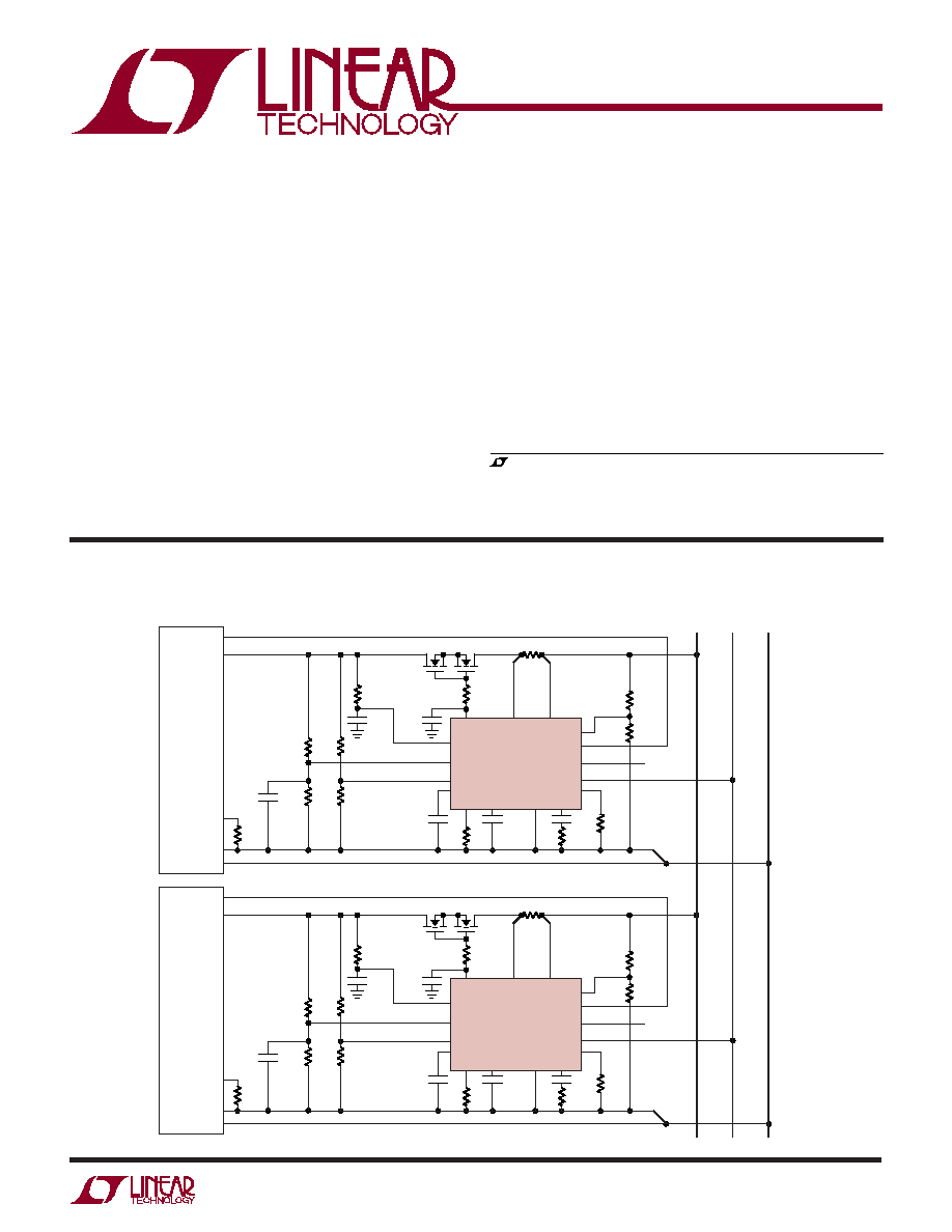
*LOAD SHARING CIRCUIT WORKS WITH MOST POWER SUPPLIES THAT HAVE A SENSE
+
OR FB PIN
470k
0.1µF
VICOR*
VI-J30-CY
SENSE
+
OUT
+
SENSE
TRIM
OUT
0.1µF
12.1k
121k
43.2k
274k
5V Load Share (5A per Module)
APPLICATIO S
U
FEATURES
TYPICAL APPLICATIO
U
DESCRIPTIO
U
2
LTC4350
4350fa
ORDER PART
NUMBER
(Note 1)
Supply Voltage (V
CC
) ............................................... 17V
Input Voltage
TIMER .................................................. 0.3V to 1.2V
R
+
, R
(Note 2) ...................................... 0.3V to 17V
FB ........................................................ 0.3V to 5.3V
OV, UV ....................................................... 0.3V to 17V
Output Voltage
COMP1 ................................................... 0.3V to 6V
COMP2 ................................................... 0.3V to 3V
GAIN, SB ............................................. 0.3V to 5.6V
GATE (Note 3) ........................................... 0.3V to 20V
I
OUT
, STATUS ........................................... 0.3V to 17V
R
SET .......................................................................
0.3V to 1V
Operating Temperature Range
LTC4350C ............................................... 0°C to 70°C
LTC4350I ........................................... 40°C to 85°C
Storage Temperature Range ................. 65°C to 150°C
Lead Temperature (Soldering, 10 sec).................. 300°C
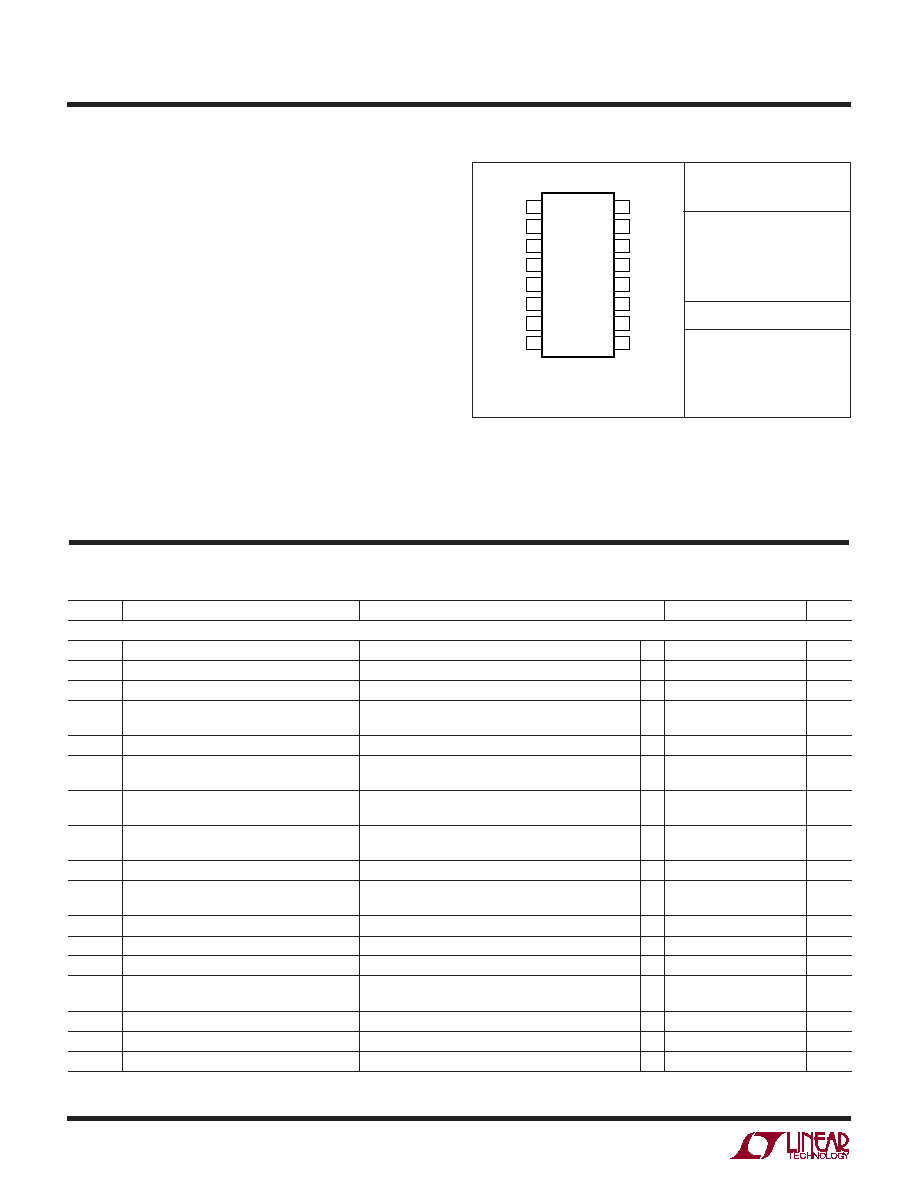
LTC4350CGN
LTC4350IGN
T
JMAX
= 150°C,
JA
= 135°C/W
ABSOLUTE
M
AXI
M
U
M
RATINGS
W
W
W
U
PACKAGE/ORDER I
N
FOR
M
ATIO
N
W
U
U
The
denotes the specifications which apply over the full operating
temperature range, otherwise specifications are at T
A
= 25°C. V
CC
= 5V unless otherwise noted.
ELECTRICAL CHARACTERISTICS
GN PACKAGE
16-LEAD PLASTIC SSOP
1
2
3
4
5
6
7
8
TOP VIEW
16
15
14
13
12
11
10
9
UV
OV
TIMER
GAIN
COMP2
COMP1
SB
GND
V
CC
STATUS
GATE
R
+
R
I
OUT
R
SET
FB
GN PART MARKING
4350
4350I
Consult LTC marketing for parts specified with wider operating temperature ranges.
Note 1: A
SYMBOL
PARAMETER
CONDITIONS
MIN
TYP
MAX
UNITS
DC Characteristics
I
CC
V
CC
Supply Current
UV = V
CC
1.0
1.6
2.0
mA
V
LKOH
V
CC
Undervoltage Lockout High
2.36
2.45
2.52
V
V
LKOL
V
CC
Undervoltage Lockout Low
2.24
2.34
2.44
V
V
FB
FB Pin Voltage
0°C to 85°C (LTC4350I) or 0°C to 70°C (LTC4350C)
1.208
1.220
1.236
V
40°C to 85°C (LTC4350I)
1.196
1.220
1.244
V
V
FBLIR
FB Line Regulation
V
CC
= 3.3V to 12V, COMP1 = 1.240V
0.02
0.05
%/V
V
FBLOR
FB Load Regulation
COMP1 = 2V
0.0008 0.1
%
COMP1 = 0.64V
0.003
0.1
%
V
UVTH
UV Pin Threshold
High Going Threshold
1.215
1.244
1.258
V
Low Going Threshold
1.205
1.220
1.237
V
V
OVTH
OV Pin Threshold
High Going Threshold
1.203
1.220
1.250
V
Low Going Threshold
1.180
1.205
1.229
V
V
TM
TIMER Pin Threshold
1.18
1.22
1.26
V
I
TM
TIMER Pin Current
TIMER On, V
TIMER
= 0V
1.75
2
2.3
µA
TIMER On, V
TIMER
= 0V, V
OV
> V
OVTH
5.30
6
6.7
µA
V
G
GAIN Pin Voltage
R
GAIN
= 25k, (V
R
+
V
R
) = 100mV
2.3
2.5
2.7
V
V
GO
GAIN Pin Offset
R
GAIN
= 25k, (V
R
+
V
R
) = 0mV
0
0.02
0.20
V
V
SB(MIN)
SB Pin Minimum Voltage
2
8
mV
V
SB(MAX)
SB Pin Maximum Voltage
V
CC
= 3.3V
2.4
2.7
2.9
V
V
CC
= 12V
5.6
7.8
10.5
V
I
SB(MAX)
SB Pin Maximum Current
V
SB
= 0V
8
33
41
mA
R
SB
SB Pin Resistor Value
14
20
33
k
V
E/A2OFF
E/A2 Offset
V
SB
V
GAIN
8
25
50
mV
3
LTC4350
4350fa
The
denotes the specifications which apply over the full operating
temperature range, otherwise specifications are at T
A
= 25°C. V
CC
= 5V unless otherwise noted.
ELECTRICAL CHARACTERISTICS
TYPICAL PERFOR A CE CHARACTERISTICS
U
W
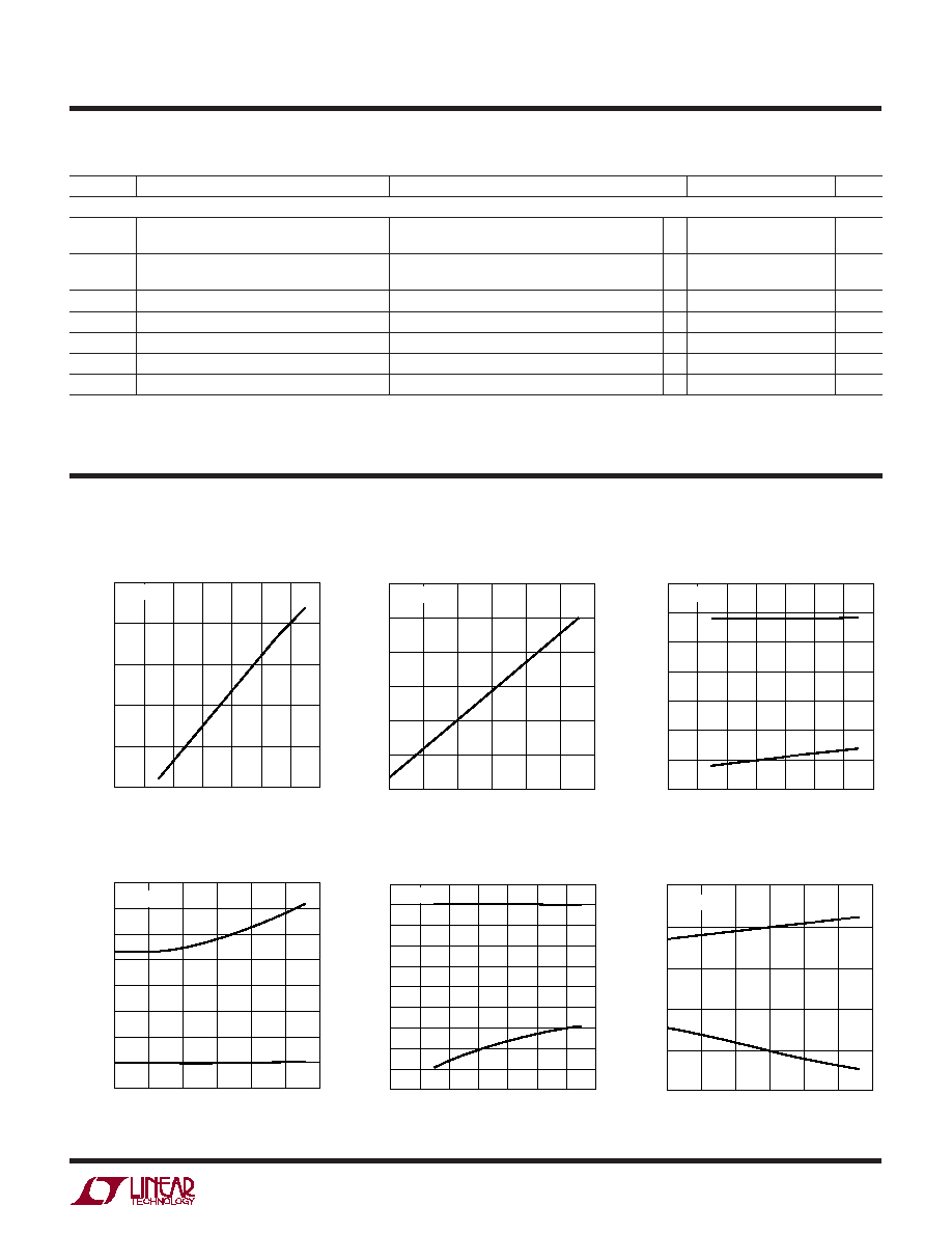
I
CC
vs V
CC
V
CC
(V)
0
2
1.0
I
CC
(mA)
2.0
3.5
4
8
10
4350 G01
1.5
3.0
2.5
6
12
14
T
A
= 25°C
TEMPERATURE (°C)
50
1.66
1.64
1.62
1.60
1.58
1.56
1.54
25
75
4350 G02
25
0
50
100
I
CC
(mA)
V
CC
= 5V
V
CC
(V)
0
2
UV THRESHOLD (V)
1.250
1.245
1.240
1.235
1.230
1.225
1.220
1.215
4
8
10
4350 G03
6
12
14
T
A
= 25°C
I
CC
vs Temperature
UV Threshold vs V
CC
UV Threshold vs Temperature
OV Threshold vs V
CC
OV Threshold vs Temperature
TEMPERATURE (°C)
50
UV THRESHOLD (V)
1.255
1.250
1.245
1.240
1.235
1.230
1.225
1.220
1.215
25
0
25
50
4350 G04
75
100
V
CC
= 5V
V
CC
(V)
0
2
OV THRESHOLD (V)
1.222
1.220
1.218
1.216
1.214
1.212
1.210
1.208
1.206
1.204
1.202
4
8
10
4350 G05
6
12
14
T
A
= 25°C
TEMPERATURE (°C)
50
OV THRESHOLD (V)
1.225
1.220
1.215
1.210
1.205
1.200
25
0
25
50
4350 G06
75
100
V
CC
= 5V
Note 1: Absolute Maximum Ratings are those values beyond which the life
of a device may be impaired.
Note 2: R
+
and R
could be at 17V while V
CC
= 0V.
SYMBOL
PARAMETER
CONDITIONS
MIN
TYP
MAX
UNITS
DC Characteristics
V
RSET(MAX)
R
SET
Pin Maximum Voltage
V
CC
= 3.3V, R
SET
= 100
0.94
1
1.03
V
V
CC
= 12V, R
SET
= 100
0.94
1
1.03
V
V
RSET(MIN)
R
SET
Pin Minimum Voltage
V
CC
= 5V, R
SET
= 1000
0.001
0.5
V
V
CC
= 5V, R
SET
= 100
0.001
0.5
V
I
RSET(MAX)
R
SET
Pin Maximum Current
R
SET
= 50, V
IOUT
= 1.1V
18
20
21
mA
V
RCTH
Reverse Current Threshold
V
R
+
V
R
+
10
30
40
mV
V
GATE
External N-Channel Gate Drive
V
GATE
V
CC
10.8
12
12.7
V
I
GATE
GATE Pin Current
Gate On, V
GATE
= 0V
8
10
12
µA
V
SOL
STATUS Pin Output Low
I
OUT
= 3mA
0.1
0.3
1.2
V
Note 3: An internal clamp limits the GATE pin to a minimum of 10.8V
above V
CC
. Driving this pin to voltages beyond the clamp may damage the
part.
4
LTC4350
4350fa
U
U
U
PI FU CTIO S
TYPICAL PERFOR A CE CHARACTERISTICS
U
W
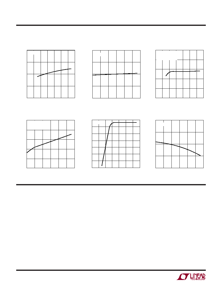
FB vs V
CC
FB vs Temperature
Gain PIn Voltage vs V
CC
Gain Pin Voltage vs Temperature
V
GATE
vs V
CC
V
GATE
vs Temperature
V
CC
(V)
0
2
1.210
FB (V)
1.230
4
8
10
4350 G07
1.215
1.225
1.220
6
12
14
T
A
= 25°C
TEMPERATURE (°C)
50
1.210
FB (V)
1.215
1.220
1.225
1.230
25
0
25
50
4350 G08
75
100
V
CC
= 5V
V
CC
(V)
0
2
2.2
GAIN (V) 2.4
2.7
4
8
10
4350 G09
2.3
2.6
2.5
6
12
14
R
GAIN
= 25k
(V
R
+
V
R
) = 100mV
T
A
= 25°C
TEMPERATURE (°C)
50
2.2
GAIN (V)
2.3
2.4
2.5
2.6
2.7
25
0
25
50
4350 G10
75
100
R
GAIN
= 25k
(V
R
+
V
R
) = 100mV
V
CC
= 5V
V
CC
(V)
0
10
11
13
6
10
4350 G11
9
8
2
4
8
12
14
7
6
12
V
GATE
(V)
T
A
= 25°C
TEMPERATURE (°C)
50
11.0
V
GATE
(V)
11.5
12.0
12.5
13.0
25
0
25
50
4350 G12
75
100
V
CC
= 5V
UV (Pin 1): Undervoltage Pin. The threshold is set at
1.244V with a 24mV hysteresis. When the UV pin is pulled
high, the charge pump ramps the GATE pin. When the UV
pin is pulled low, the GATE pin will be pulled low.
OV (Pin 2): Overvoltage Pin. The threshold is set at 1.220V
with a 15mV hysteresis. When the OV pin is pulled high,
the GATE pin is pulled low. After a timer cycle, the STATUS
pin is pulled low until the OV pin is pulled low.
TIMER (Pin 3): Analog System Timing Generator Pin. This
pin is used to set the delay before the load sharing turns
on after the UV pin goes high. The other use for the TIMER
pin is to delay the indication of a fault on the STATUS pin.
When the timer is off, an internal N-channel shorts the
TIMER pin to ground. When the timer is turned on, a 2µA
or 6µA timer current (I
TIMER
) from V
CC
is connected to the
TIMER pin and the voltage starts to ramp up with a slope
given by: dV/dt = I
TIMER
/C
T
. When the voltage reaches the
trip point (1.220V), the timer will be reset by pulling the
TIMER pin back to ground. The timer period is given by:
(1.220V · C
T
)/I
TIMER
.
GAIN (Pin 4): Analog Output Pin. The voltage across the
R
+
and R
pins is divided by a 1k resistor and sourced as
a current from the GAIN pin. An external resistor on the
GAIN pin determines the voltage gain from the current
sense resistor to the GAIN pin.
5
LTC4350
4350fa
U
U
U
PI FU CTIO S
COMP2 (Pin 5): Analog Output Pin. This pin is the output
of the share bus error amplifier E/A2. (A compensation
capacitor between this pin and ground sets the crossover
frequency for the power supply adjustment loop.) In most
cases, this pin operates between 0.5V to 1.5V and repre-
sents a diode voltage up from the voltage at the R
SET
pin.
It is clamped at 3V. During start-up, this pin is clamped to
ground. After a timer cycle (and if the GATE pin is high), the
COMP2 pin is released.
COMP1 (Pin 6): Analog Output Pin. This pin is the output
of the voltage regulating error amplifier E/A1. A compen-
sation capacitor between this pin and ground sets the
crossover frequency of the share bus loop. This pin
operates a diode voltage up from the voltage at the SB pin
and is clamped at 8.4V.
SB (Pin 7): Analog Output Pin. This pin drives the share
bus used to communicate the value of shared load current
between several power supplies. There is an amplifier that
drives this pin a diode below the COMP1 pin using an
internal NPN as a pull-up and a 20k resistor as a pull-down.
GND (Pin 8): Chip Ground.
FB (Pin 9): Analog Error Amplifier Input (E/A1). This pin is
used to monitor the output supply voltage with an external
resistive divider. The FB pin voltage is compared to 1.220V
reference. The difference between the FB pin voltage and
the reference is amplified and output on the COMP1 pin.
R
SET
(Pin 10): Analog Output Pin. The I
OUT
amplifier
converts the voltage at the COMP2 pin (down a diode
voltage) to the R
SET
pin. Therefore, the current through the
external resistor (R
SET
) placed between the R
SET
pin and
ground is (COMP2 V
DIODE
)/R
SET
. This current is used to
adjust the output voltage.
I
OUT
(Pin 11): Analog Output Pin. The current flowing into
the I
OUT
pin is equal to the current flowing out of the R
SET
pin that was set by the external resistor R
SET
. This current
is used to adjust the output supply voltage by modifying
the voltage sensed by the power supply's internal voltage
feedback circuitry.
R
(Pin 12): Analog Input Pin. With a sense resistor placed
in the supply path between the R
+
and R
pins, the power
supply current is measured as a voltage drop between R
+
and R
. This voltage is measured by the I
SENSE
block and
multiplied at the GAIN pin.
R
+
(Pin 13): Analog Input Pin. With a sense resistor placed
in the supply path between the R
+
and R
pins, the power
supply current is measured as a voltage drop between R
+
and R
. This voltage is measured by the I
SENSE
block and
multiplied at the GAIN pin.
GATE (Pin14): The high side gate drive for the external
N-Channel power FET. An internal charge pump provides
the gate drive necessary to drive the FETs. The slope of the
voltage rise or fall at the GATE is set by an external
capacitor connected between GATE and GND, and the
10µA charge pump output current. When the undervoltage
lockout circuit monitoring V
CC
trips, the OV pin is pulled
high or the UV pin is pulled low, the GATE pin is immedi-
ately pulled to GND.
STATUS (Pin 15): Open-Drain Digital Output. The STA-
TUS pin has an open-drain output to GND. This pin is
pulled low to indicate a fault has occurred in the system.
There are three types of faults. The first is a undervoltage
lockout on V
CC
or the UV pin is low while the output
voltage is active. The second is when the COMP2 pin is
above 1.5V or below 0.5V and the voltage on the GAIN pin
is greater than 100mV. The final failure is when the OV pin
is high. The three faults will activate the pull-down on the
STATUS pin after a timing cycle.
V
CC
(Pin 16): The Positive Supply Input, Ranging from
3.3V to 12V for Normal Operation. I
CC
is typically 1.6mA.
An undervoltage lockout circuit disables the chip until the
voltage at V
CC
is greater than 2.47V. A 0.1µF bypass
capacitor is required on the V
CC
pin. If the V
CC
pin is tied
to the same power supply output that is being adjusted,
then a 51 decoupling resistor is needed to hold up the
supply during a short to ground on the supply output. V
CC
must be greater than or equal to the supply that is
connected to the R
+
and R
pins.