 | –≠–ª–µ–∫—Ç—Ä–æ–Ω–Ω—ã–π –∫–æ–º–ø–æ–Ω–µ–Ω—Ç: LTC4351 | –°–∫–∞—á–∞—Ç—å:  PDF PDF  ZIP ZIP |
1
LTC4413
4413f
Dual 2.6A, 2.5V to 5.5V,
Ideal Diodes in 3mm ◊ 3mm DFN
2-Channel Ideal Diode ORing or Load Sharing
Low Loss Replacement for ORing Diodes
Low Forward ON Resistance (100m Max at 3.6V)
Low Reverse Leakage Current (1µA Max)
Small Regulated Forward Voltage (28mV Typ)
2.5V to 5.5V Operating Range
2.6A Maximum Forward Current
Internal Current Limit and Thermal Protection
Slow Turn-Off to Protect Against Inductive Source
Impedance-Induced Voltage Spiking
Low Quiescent Current
Status Output to Indicate if Selected Channel is
Conducting
Programmable Channel ON/OFF
Low Profile (0.75mm) 10-Lead 3mm ◊ 3mm DFN
Package
DESCRIPTIO
U
FEATURES
The LTC
Æ
4413 contains two monolithic ideal diodes, each
capable of supplying up to 2.6A from input voltages be-
tween 2.5V and 5.5V. Each ideal diode uses a 100m
P-channel MOSFET that independently connects INA to
OUTA and INB to OUTB. During normal forward operation
the voltage drop across each of these diodes is regulated
to as low as 28mV. Quiescent current is less than 40µA for
diode currents up to 1A. If either of the output voltages
exceeds its respective input voltages, that MOSFET is turned
off and less than 1µA of reverse current will flow from OUT
to IN. Maximum forward current in each MOSFET is lim-
ited to a constant 2.6A and internal thermal limiting cir-
cuits protect the part during fault conditions.
Two active-high control pins independently turn off the
two ideal diodes contained within the LTC4413, control-
ling the operation mode as described by Table 3. When the
selected channel is reverse biased, or the LTC4413 is put
into low power standby, a status signal indicates this con-
dition with a low voltage.
A 9µA open-drain STAT pin is used to indicate conduction
status. When terminated to a positive supply through a 470k
resistor, the STAT pin can be used to indicate that the se-
lected diode is conducting with a HIGH voltage. This signal
can also be used to drive an auxiliary P-channel MOSFET
power switch to control a third alternate power source when
the LTC4413 is not conducting forward current.
The LTC4413 is housed in a 10-lead DFN package.
Battery and Wall Adapter Diode ORing in Handheld
Products
Backup Battery Diode ORing
Power Switching
USB Peripherals
Uninterruptable Supplies
APPLICATIO S
U
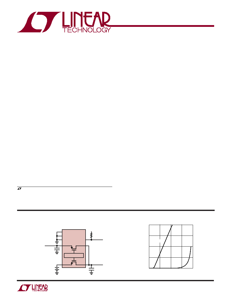
TYPICAL APPLICATIO
U
ENBA
GND
ENBB
470k
V
CC
INA
BAT
10µF
4.7µF
4413 TA01
TO LOAD
STAT IS HIGH WHEN
BAT IS SUPPLYING
LOAD CURRENT
WALL
ADAPTER
(0V TO 5.5V)
OUTA
INB
OUTB
STAT
CONTROL CIRCUIT
LTC4413
V
FWD
(mV)
0
I
OUT
(mA) 1000
1500
400
4413 TA01b
500
0
100
200
300
2000
LTC4413
1N5817
LTC4413 vs 1N5817 Schottky
, LTC and LT are registered trademarks of Linear Technology Corporation.
All other trademarks are the property of their respective owners.

2
LTC4413
4413f
ORDER PART
NUMBER
(Note 1)
INA, INB, OUTA, OUTB, STAT,
ENBA, ENBB Voltage ................................... ≠0.3V to 6V
Operating Temperature Range ................ ≠ 40∞C to 85∞C
Storage Temperature Range ................. ≠ 65∞C to 125∞C
Continuous Power Dissipation
(Derate 25mW/∞C Above 70∞C) ....................... 1500mW
LTC4413EDD
T
JMAX
= 125∞C,
JA
= 40∞C/W (4-LAYER PCB)
EXPOSED PAD (PIN 11) IS GND
MUST BE SOLDERED TO PCB
ABSOLUTE
M
AXI
M
U
M
RATINGS
W
W
W
U
PACKAGE/ORDER I
N
FOR
M
ATIO
N
W
U
U
Consult LTC Marketing for parts specified with wider operating temperature ranges.
DD PART
MARKING
LBGN
The
indicates specifications which apply over the full operating
temperature range, otherwise specifications are at T
A
= 25∞C. (Notes 2, 6)
ELECTRICAL CHARACTERISTICS
SYMBOL
PARAMETER
CONDITIONS
MIN
TYP
MAX
UNITS
V
IN
, V
OUT
Operating Supply Range for Channel A or B
V
IN
and/or V
OUT
Must be in This Range
2.5
5.5
V
for Proper Operation
UVLO
UVLO Turn-On Rising Threshold
Max (V
INA
, V
INB
, V
OUTA
, V
OUTB
)
2.4
V
UVLO Turn-Off Falling Threshold
Max (V
INA
, V
INB
, V
OUTA
, V
OUTB
)
1.7
V
I
QF
Quiescent Current in Forward Regulation (Note 3) V
INA
= 3.6V, I
OUTA
= ≠100mA, V
INB
= 0V,
25
30
µA
I
OUTB
= 0mA
I
LEAK
Current Drawn from or Sourced into IN when
V
IN
= 3.6V, V
OUT
= 5.5V (Note 6)
≠1
0.5
2
µA
V
OUT
is Greater than V
IN
I
QRGND
Quiescent Current While in Reverse Turn-Off,
V
INA
, V
INB
, V
OUTB
< V
OUTA
= 5.5V,
22
30
µA
Measured via GND
V
STAT
= 0V
I
QROUTA
Quiescent Current While in Reverse Turn-Off,
V
INA
, V
INB
, V
OUTB
< V
OUTA
= 5.5V
17
23
µA
Current Drawn from V
OUTA
when OUTA
Supplies Chip Power
I
QROUTB
Quiescent Current While in Reverse Turn-Off,
V
INA
, V
INB
, V
OUTA
< V
OUTB
= 5.5V
2
3
µA
Current Drawn from V
OUTA
when OUTB
Supplies Chip Power
I
QOFF
Quiescent Current with Both ENBA
V
INA
= V
INB
= 3.6V, V
ENBA
and
20
27
µA
and ENBB High
V
ENBB
High, V
STAT
= 0V
V
RTO
Reverse Turn-Off Voltage (V
OUT
≠ V
IN
)
V
IN
= 3.6V
≠5
10
mV
V
FWD
Forward Voltage Drop (V
IN
≠ V
OUT
)
V
IN
= 3.6V
28
38
mV
at I
OUT
= ≠1mA
R
FWD
On Resistance, R
FWD
Regulation
V
IN
= 3.6V, I
OUT
= ≠100mA
140
m
(Measured as V/I)
V
IN
= 3.6V, I
OUT
= ≠500mA (Note 5)
100
m
R
ON
On Resistance, R
ON
Regulation
V
IN
= 3.6V, I
OUT
= ≠1.5A (Note 5)
140
200
m
(Measured as V/I at I
IN
= 1A)
t
OFF
PowerPath
TM
Turn-Off Time
V
IN
= 3.6V, I
OUT
= ≠100mA
4
µs
PowerPath is a trademark of Linear Technology Corporation.
TOP VIEW
11
DD PACKAGE
10-LEAD (3mm ◊ 3mm) PLASTIC DFN
10
9
6
7
8
4
5
3
2
1
OUTA
STAT
NC
NC
OUTB
INA
ENBA
GND
ENBB
INB
3
LTC4413
4413f
The
indicates specifications which apply over the full operating
temperature range, otherwise specifications are at T
A
= 25∞C. (Notes 2, 6)
ELECTRICAL CHARACTERISTICS
Note 1: Absolute Maximum Ratings are those values beyond which the life
of a device may be impaired.
Note 2: The LTC4413 is guaranteed to meet performance specifications
from 0∞C to 70∞C. Specifications over the ≠40∞C to 85∞C ambient
operating temperature range are assured by design, characterization and
correlation with statistical process controls.
Note 3: Quiescent current increases with diode current, refer to plot of I
QF
vs I
OUT
.
Note 4: This IC includes overtemperature protection that is intended to
protect the device during momentary overload conditions.
Overtemperature protection will become active at a junction temperature
greater than the maximum operating temperature. Continuous operation
above the specified maximum operating junction temperature may impair
device reliability.
Note 5: This specification is guaranteed by correlation to wafer-level
measurements.
Note 6: Unless otherwise specified, current into a pin is positive and
current out of a pin is negative. All voltages referenced to GND.
SYMBOL
PARAMETER
CONDITIONS
MIN
TYP
MAX
UNITS
Short-Circuit Response
I
OC
Current Limit
V
INX
= 3.6V (Notes 4, 5)
1.8
A
I
QOC
Quiescent Current While in
V
INX
= 3.6V, I
OUT
= 1.9A (Notes 4, 5)
150
300
µA
Overcurrent Operation
STAT Output
I
SOFF
STAT Off Current
Shutdown
≠1
0
1
µA
I
SON
STAT Sink Current
V
IN
> V
OUT
, V
CTL
< V
IL
, I
OUT
< I
MAX
7
9
13
µA
t
S(ON)
STAT Pin Turn-On Time
1
µs
t
S(OFF)
STAT Pin Turn-Off Time
1
µs
ENB Inputs
V
ENBIH
ENB Inputs Rising Threshold Voltage
V
ENB
Rising
540
600
mV
V
ENBIL
ENB Inputs Falling Threshold Voltage
V
ENB
Falling
400
460
mV
V
ENBHYST
ENB Inputs Hysteresis
V
ENBHYST
= (V
ENBIH
≠ V
ENBIL
)
90
mV
I
ENB
ENB Inputs Pull-Down Current
V
OUT
< V
IN
= 3.6V, V
ENB
> V
ENBIL
1.5
3
4.5
µA

4
LTC4413
4413f
TYPICAL PERFOR A CE CHARACTERISTICS
U
W
I
QF
vs I
LOAD
I
QF
vs I
LOAD
I
QF
vs Temperature
I
OC
vs Temperature (V
IN
= 3.5V)
UVLO Thresholds vs Temperature
R
FWD
vs V
IN
at I
LOAD
= 500mA
R
FWD
vs Temperature (V
IN
= 3.5V)
V
FWD
and R
FWD
vs I
LOAD
V
FWD
and R
FWD
vs I
LOAD
I
LOAD
(A)
40
I
QF
(
µ
A)
80
120
160
200
100E-6
10E-3
100E-3
10E+0
4413 G01
0
1E-3
1E+0
120∞C
80∞C
40∞C
0∞C
≠40∞C
I
LOAD
(A)
0
0
I
QF
(
µ
A)
40
80
120
160
200
0.50
1
1.50
2
4413 G02
2.50
3
120∞C
80∞C
40∞C
0∞C
≠40∞C
TEMPERATURE (∞C)
≠40
I
QF
(
µ
A)
40
60
120
4413 G03
20
0
0
40
80
80
I
QF
AT 1A
I
QF
AT 100mA
TEMPERATURE (∞C)
≠40
1
I
OC
(A)
2
3
4
0
40
80
120
4413 G04
TEMPERATURE (∞C)
≠40
2.05
2.10
2.20
80
4413 G05
2.00
1.95
0
40
120
1.90
1.85
2.15
UVLO (V)
UVLO TURN-ON
UVLO TURN-OFF
V
INA
(V)
2.5
0
R
FWD
(m
)
20
40
60
80
120
3.5
4.5
4413 G06
5.5
100
120∞C
80∞C
≠40∞C
0∞C
40∞C
TEMPERATURE (∞C)
≠60
R
FWD
(m
)
60
80
100
60
140
4413 G07
40
20
0
≠20
20
100
120
140
160
RFWD I
OUT
= 100mA
RFWD I
OUT
= 500mA
RFWD I
OUT
= 1A
I
OUT
(mA)
0
500
1500
2500
1000
2000
3000
0
V
FWD
(mV) AND R
FWD
(m
)
50
100
150
200
300
250
V
FWD
R
FWD
4413 G08
120∞C
80∞C
40∞C
0∞C
≠40∞C
I
LOAD
(mA)
1
10
100
1000
10000
0
V
FWD
(mV) AND R
FWD
(m
)
50
100
150
200
300
250
4413 G09
120∞C
80∞C
40∞C
0∞C
≠40∞C
V
FWD
R
FWD

5
LTC4413
4413f
TYPICAL PERFOR A CE CHARACTERISTICS
U
W
V
FWD
vs I
LOAD
(V
IN
= 3.5V)
ENB Turn-On
ENB Turn-Off
ENB Threshold vs Temperature
ENB Hysteresis vs Temperature
≠ I
LEAK
vs Temperature at
V
REVERSE
= 5.5V
I
LOAD
(mA)
50
V
FWD
(mV)
100
150
200
300
250
1
100
1000
10000
4413 G10
0
10
120∞C
80∞C
40∞C
0∞C
≠40∞C
20µs/DIV
4413 G12
CH4 = I
OUT
(200mA/DIV)
CH3 = V
OUT
(2V/DIV)
CH2 = V
STAT
(2V/DIV)
CH1 = V
ENBA
(500mV/DIV)
CH1
CH2
CH3
CH4
TEMPERATURE (∞C)
≠40
ENB THRESHOLD (mV)
450
500
550
V
IH
V
IL
120
4413 G13
400
350
300
0
40
80
TEMPERATURE (∞C)
≠40
0
ENB HYSTERESIS (mV)
20
40
60
80
100
120
0
40
80
120
4413 G14
TEMPERATURE (∞C)
10E-9
≠I
LEAK
(A)
100E-9
1E-6
10E-6
≠40
40
80
120
1E-9
0
4413 G15
≠ I
LEAK
vs V
REVERSE
V
REVERSE
(V)
10E-9
≠I
LEAK
(A)
100E-9
1E-6
10E-6
0
2
4
3
5
1E-9
1
4413 G16
80∞C
40∞C
0∞C
≠40∞C
400µs/DIV
4413 G11
CH4 = I
OUT
(500mA/DIV)
CH3 = V
OUT
(2V/DIV)
CH2 = V
STAT
(2V/DIV)
CH1 = V
ENBA
(500mV/DIV)
CH1
CH2
CH3
CH4
CH4
CH3
CH2
CH1