4403i.pm6
1
LTC4403-1/LTC4403-2
4403i
Multiband RF Power
Controllers for EDGE/TDMA
January 2003
The LTC
®
4403-2 is a multiband RF power controller for
RF power amplifiers operating in the 800MHz to 2.4GHz
range. The LTC4403-2 has two outputs to control dual T
X
PA modules with two control inputs. An internal sample
and hold circuit enables the LTC4403-2 to be used with
AM modulation via the carrier or PA supply. The input
voltage range is optimized for operation from a single
lithium-ion cell or 3
×
NiMH.
RF power is controlled by driving the RF amplifier power
control pins and sensing the resultant RF output power.
The RF sense voltage is peak detected using an on-chip
Schottky diode. This detected voltage is compared to the
DAC voltage at the PCTL pin to control the output power.
The LTC4403-1 is a single output RF power controller
with identical performance to the LTC4403-2. The
LTC4403-1 has one output to control a single T
X
PA or
dual T
X
PA module with a single control input and is
available in an 8-pin MSOP package.
Internal and external offsets are cancelled over tempera-
ture by an autozero control loop. The shutdown feature
disables the part and reduces the supply current to
< 10
µ
A.
s
Supports AM Modulation in EDGE/TDMA (ANSI-136)
Applications
s
Single Output RF Power Amplifier Control
(LTC4403-1)
s
Dual Output RF Power Amplifier Control (LTC4403-2)
s
Internal Schottky Diode Detector with >40dB Range
s
Wide Input Frequency Range: 800MHz to 2.4GHz
s
Autozero Loop Cancels Offset Errors and
Temperature Dependent Offsets
s
Wide V
IN
Range: 2.7V to 6V
s
Allows Direct Connection to Battery
s
RF Output Power Set by External DAC
s
Internal Frequency Compensation
s
Rail-to-Rail Power Control Outputs
s
Low Operating Current: 1mA
s
Low Shutdown Current: < 10
µ
A
s
PCTL Input Filter
s
Available in a 8-Pin MSOP Package (LTC4403-1)
and 10-Pin MSOP (LTC4403-2)
, LTC and LT are registered trademarks of Linear Technology Corporation.
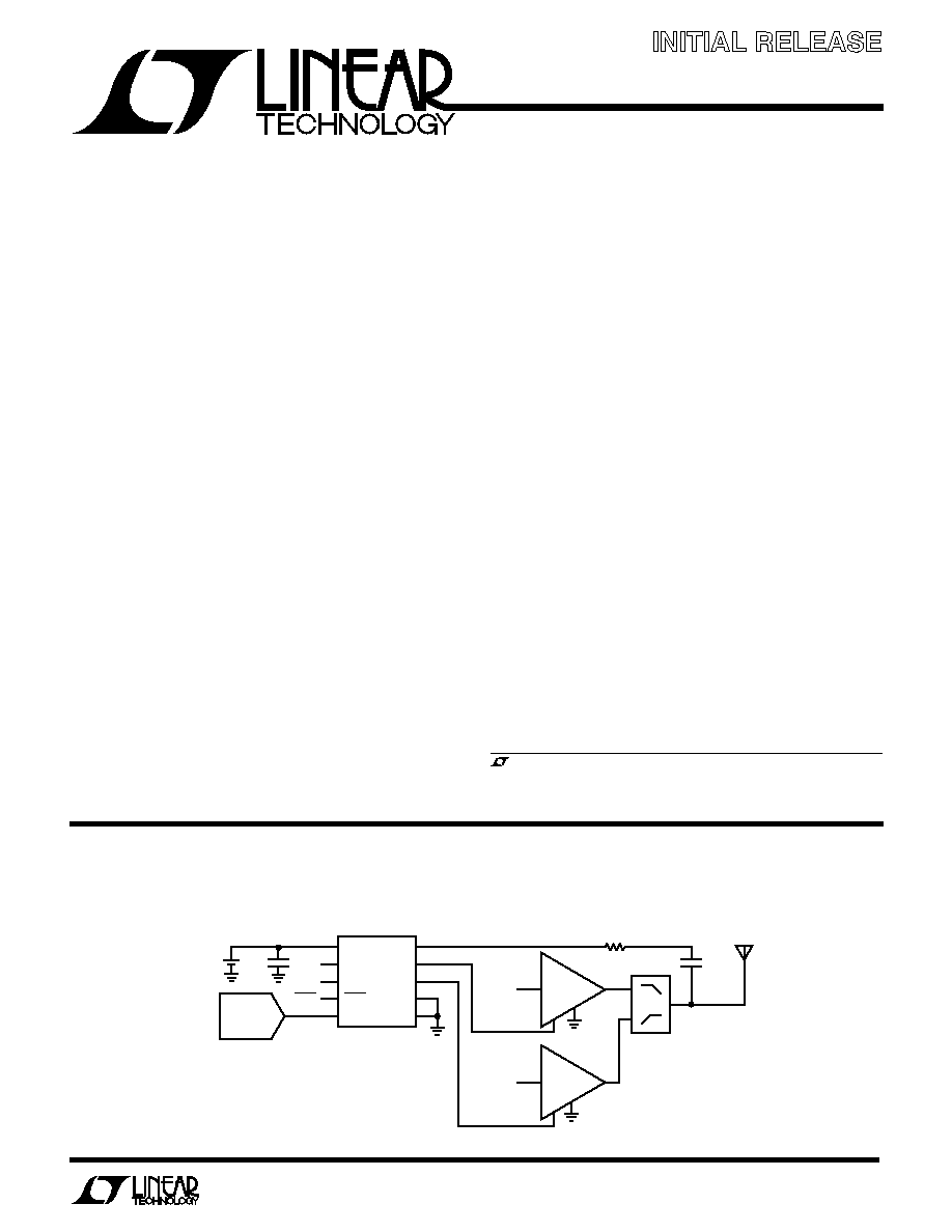
LTC4403-2 Multiband EDGE Cellular Telephone Transmitter
s
Multiband GSM/GPRS/EDGE Cellular
Telephones
s
PCS Devices
s
Wireless Data Modems
s
U.S. TDMA Cellular Phones
Information furnished by Linear Technology Corporation is believed to be accurate and reliable.
However, no responsibility is assumed for its use. Linear Technology Corporation makes no represen-
tation that the interconnection of its circuits as described herein will not infringe on existing patent rights.
FEATURES
DESCRIPTIO
U
APPLICATIO S
U
TYPICAL APPLICATIO
U
Final Electrical Specifications
V
IN
BSEL
V
HOLD
SHDN
PCTL
1
9
8
7
6
10
2
3
4
5
RF
V
PCA
V
PCB
GND
GND
LTC4403-2
0.4pF
±
0.05pF
Li-Ion
SHDN
BSEL
850MHz/
900MHz
DAC
RF PA
DIPLEXER
1.8GHz /
1.9GHz
RF PA
50
4403 TA01
V
HOLD
0.1
µ
F
2
LTC4403-1/LTC4403-2
4403i
PARAMETER
CONDITIONS
MIN
TYP
MAX
UNITS
V
IN
Operating Voltage
q
2.7
6
V
I
VIN
Shutdown Current
SHDN = 0V
q
10
20
µ
A
I
VIN
Operating Current
I
VPCA
= I
VPCB
= 0mA
q
1.5
2
mA
V
PCA/B
V
OL
R
LOAD
= 400
, Enabled
q
0
0.1
V
V
PCA/B
Dropout Voltage
I
LOAD
= 6mA, V
IN
= 2.7V
q
V
IN
0.25
V
V
PCA/B
Output Current
V
PCA/B
= 2.4V, V
IN
= 2.7V,
V
OUT
= 10mV
q
6
mA
V
PCA/B
Enable Time
SHDN = High (Note 5)
q
9
11
µ
s
V
PCA/B
Bandwidth
C
LOAD
= 33pF, R
LOAD
= 400 (Note 7)
PCTL < 80mV
250
kHz
PCTL > 160mV
130
kHz
V
PCA/B
Load Capacitance
(Note 6)
q
100
pF
V
PCA/B
Slew Rate
V
PCTL
= 2V Step, C
LOAD
= 100pF, R
LOAD
= 400 (Note 3)
1.4
V/
µ
s
V
PCA/B
V
HOLD
Droop
Unity Gain, V
PCTL
= 2V, V
HOLD
= High
1
µ
V/ms
V
HOLD
Time
Time from V
HOLD
High to Hold Switch Opening
100
ns
V
PCA/B
Start Voltage
Open Loop
q
250
450
550
mV
V
PCA/B
Voltage Clamp
PCTL = 1V, V
IN
= 5V
q
3.6
4
4.4
V
SHDN, V
HOLD
, BSEL Input Threshold Low
V
IN
= 2.7V to 6V
q
0.35
V
SHDN, V
HOLD
, BSEL Input Threshold High
V
IN
= 2.7V to 6V
q
1.4
V
SHDN, BSEL, V
HOLD
Input Current
SHDN, BSEL, V
HOLD
= V
IN
= 3.6V
q
16
24
36
µ
A
PCTL Input Voltage Range
(Note 4)
q
0
2.4
V
PCTL Input Resistance
q
60
90
120
k
V
IN
to GND ............................................... 0.3V to 6.5V
V
PCA
, V
PCB
Voltage .................................. 0.3V to 4.6V
PCTL Voltage ............................... 0.3V to (V
IN
+ 0.3V)
RF Voltage ........................................ (V
IN
±
2.6V) to 7V
SHDN, V
HOLD
, BSEL Voltage
to GND ......................................... 0.3V to (V
IN
+ 0.3V)
ORDER PART
NUMBER
MS PART MARKING
LTC4403-2EMS
LTXJ
T
JMAX
= 125
°
C,
JA
= 160
°
C/W
I
VPCA/B ..................................................................................
10mA
Operating Temperature Range (Note 2) .. 40
°
C to 85
°
C
Storage Temperature Range ................ 65
°
C to 150
°
C
Maximum Junction Temperature ........................ 125
°
C
Lead Temperature (Soldering, 10 sec)................ 300
°
C
(Note 1)
ORDER PART
NUMBER
MS8 PART MARKING
LTC4403-1EMS8
LTXG
The
q
denotes specifications which apply over the full operating
temperature range, otherwise specifications are at T
A
= 25
°
C. V
IN
= 3.6V, SHDN = V
IN
unless otherwise noted.
T
JMAX
= 125
°
C,
JA
= 160
°
C/W
ABSOLUTE AXI U RATI GS
W
W
W
U
PACKAGE/ORDER I FOR ATIO
U
U
W
ELECTRICAL CHARACTERISTICS
Consult LTC Marketing for parts specified with wider operating temperature ranges.
1
2
3
4
V
IN
V
PCA
GND
GND
8
7
6
5
RF
V
HOLD
SHDN
PCTL
TOP VIEW
MS8 PACKAGE
8-LEAD PLASTIC MSOP
1
2
3
4
5
V
IN
V
PCA
V
PCB
GND
GND
10
9
8
7
6
RF
BSEL
V
HOLD
SHDN
PCTL
TOP VIEW
MS PACKAGE
10-LEAD PLASTIC MSOP
3
LTC4403-1/LTC4403-2
4403i
PARAMETER
CONDITIONS
MIN
TYP
MAX
UNITS
PCTL Input Filter
270
kHz
Autozero Range
Maximum DAC Zero-Scale Offset Voltage
q
400
mV
that can be applied to PCTL
RF Input Frequency Range
(Note 6)
q
800
2400
MHz
RF Input Power Range
F = 900MHz (Note 6)
27 to 18
dBm
F = 1800MHz (Note 6)
25 to 18
dBm
F = 2400MHz (Note 6)
23 to 16
dBm
RF Input Resistance
Referenced to V
IN
q
150
250
350
ELECTRICAL C
C
HARA TERISTICS
The
q
denotes specifications which apply over the full operating
temperature range, otherwise specifications are at T
A
= 25
°
C. V
IN
= 3.6V, SHDN = V
IN
, unless otherwise noted.
Note 1: Absolute Maximum Ratings are those values beyond which the life
of a device may be impaired.
Note 2: Specifications are assured over the 40
°
C to 85
°
C temperature
range by design characterization and correlation with statistical process
controls.
Note 3: Slew rate is measured open loop. The rise time at V
PCA
or V
PCB
is
measured between 1V and 2V.
Note 4: Includes maximum DAC offset voltage and maximum control
voltage.
Note 5: This is the time from SHDN rising edge 50% switch point to
V
PCA/B
= 250mV.
Note 6: Guaranteed by design. This parameter is not production tested.
Note 7: Bandwidth is calculated using the 10% to 90% rise time:
BW = 0.35/rise time
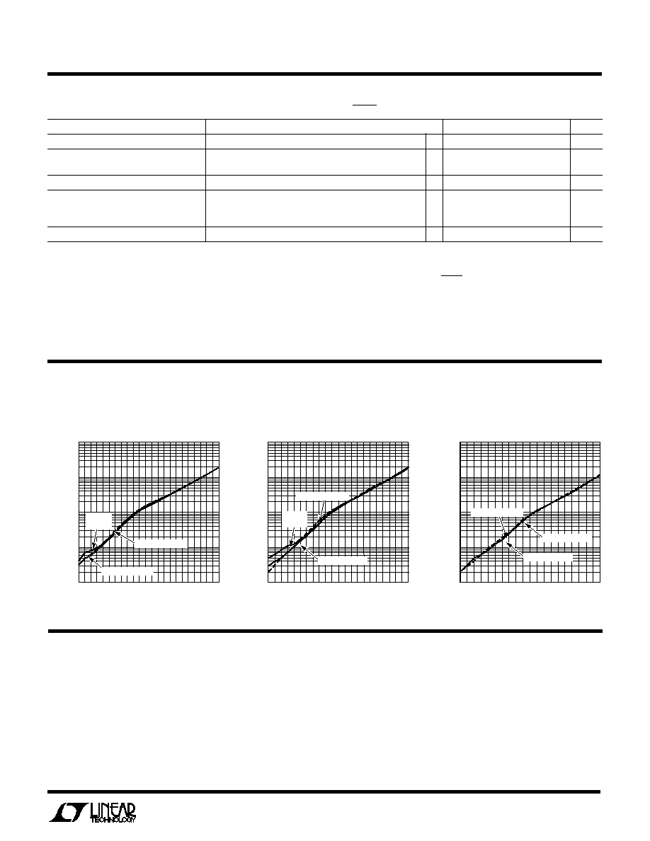
TYPICAL PERFOR A CE CHARACTERISTICS
U
W
Detector Characteristics at 900MHz
Detector Characteristics at 1800MHz
V
IN
(Pin 1): Input Supply Voltage, 2.7V to 6V. V
IN
should
be bypassed with 0.1
µ
F and 100pF ceramic capacitors.
V
PCA
(Pin 2): Power Control Voltage Output. This pin
drives an external RF power amplifier power control pin.
The maximum load capacitance is 100pF. The output is
capable of rail-to-rail swings at low load currents. Selected
when BSEL is low.
(LTC4403-1/LTC4403-2)
U
U
U
PI FU CTIO S
V
PCB
(Pin 3): (LTC4403-2 Only) Power Control Voltage
Output. This pin drives an external RF power amplifier
power control pin. The maximum load capacitance is
100pF. The output is capable of rail-to-rail swings at low
load currents. Selected when BSEL is high.
GND (Pin 3/4): System Ground.
RF INPUT POWER (dBm)
10
PCTL REFERENCED DETECTOR OUTPUT VOLTAGE (mV)
100
1000
10000
26
14
8
2
4
10
1
20
16
4403 G01
0.9GHz AT 30
°
C
0.9GHz AT 75
°
C
0.9GHz
AT 25
°
C
RF INPUT POWER (dBm)
10
PCTL REFERENCED DETECTOR OUTPUT VOLTAGE (mV)
100
1000
10000
26
14
8
2
4
10
1
20
16
4403 G02
1.8GHz AT 30
°
C
1.8GHz AT 75
°
C
1.8GHz
AT 25
°
C
RF INPUT POWER (dBm)
10
PCTL REFERENCED DETECTOR OUTPUT VOLTAGE (mV)
100
1000
10000
14
8
2
4
10
1
20
16
4403 G03
2.4GHz AT 30
°
C
2.4GHz AT 75
°
C
2.4GHz AT 25
°
C
Detector Characteristics at 2400MHz
4
LTC4403-1/LTC4403-2
4403i
GND (Pin 4/5): System Ground.
PCTL (Pin 5/6): Analog Input. The external power control
DAC drives this input. The amplifier servos the RF power
until the RF detected signal equals the DAC signal applied
at this pin.
SHDN (Pin 6/7): Shutdown Input. A logic low on the SHDN
pin places the part in shutdown mode. A logic high enables
the part after 10
µ
s. SHDN has an internal 150k pull-down
resistor to ensure that the part is in shutdown when no input
is applied.
(LTC4403-1/LTC4403-2)
U
U
U
PI FU CTIO S
V
HOLD
(Pin 7/8): Asserted high prior to AM modulation,
opens control loop and holds voltage at V
PCA
or V
PCB
during
EDGE modulation.
BSEL (Pin 9): (LTC4403-2 Only) Selects V
PCA
when low
and V
PCB
when high. This input has an internal 150k
resistor to ground.
RF (Pin 8/10): Coupled RF Feedback Voltage . This input
is referenced to V
IN
. The frequency range is 800MHz to
2400MHz. This pin has an internal 250
termination, an
internal Schottky diode detector and peak detector capaci-
tor.
BLOCK DIAGRA
W
(LTC4403-2)
+
RFDET
+
GM
70mV
270kHz
FILTER
+
30k
22k
51k
30k
250
28pF
0.4pF
±
0.05pF
12
100
100
4403 BD
12
150k
150k
150k
BSEL
PB
PA
60
µ
A
60
µ
A
RF
10
V
IN
Li-Ion
1
V
PCA
V
PCB
GND
9
PCTL
6
RF PA
850MHz/900MHz
AZ
AUTOZERO
TXENB
TXENB
V
HOLD
+
+
MUX
CONTROL
V
HOLD
8
7
SHDN
RF PA
DIPLEXER
1.8GHz/1.9GHz
5
50
9
µ
s
DELAY
GAIN
COMPRESSION
2
3
C
HOLD
V
IN
V
REF
C
REF
BUFFER
V
HOLD
V
HOLD
38k
+
4

5
LTC4403-1/LTC4403-2
4403i
APPLICATIO
N
S I
N
FOR
M
ATIO
N
W
U
U
U
Operation
The LTC4403-1/-2 single/dual band RF power controller
integrates several functions to provide RF power control
over frequencies ranging from 800MHz to 2.4GHz. These
functions include an internally compensated amplifier to
control the RF output power, an autozero section to cancel
internal and external voltage offsets, an RF Schottky diode
peak detector and amplifier to convert the RF feedback
signal to DC, a multiplexer to switch the controller output
to either V
PCA
or V
PCB
, a V
PCA/B
overvoltage clamp, com-
pression and a bandgap reference.
Band Selection
The LTC4403-2 is designed for multiband operation. The
BSEL pin will select output V
PCA
when low and output
V
PCB
when high. For example, V
PCA
could be used to drive
an 850MHz/900MHz channel and V
PCB
a 1.8GHz/1.9GHz
channel. BSEL must be established before the part is
enabled. The LTC4403-1 can be used to drive a single RF
channel or dual channel with integral multiplexer.
Control Amplifier
The control amplifier supplies the power control voltage to
the RF power amplifier. A portion (typically 19dB for low
frequencies and 14dB for high frequencies) of the RF
output voltage is coupled into the RF pin, to close the gain
control loop. When a DAC voltage is applied to PCTL, the
amplifier quickly servos V
PCA
or V
PCB
positive until the
detected feedback voltage applied to the RF pin matches
the voltage at PCTL. This feedback loop provides accurate
RF power control. V
PCA
or V
PCB
are capable of driving a
6mA load current and 100pF load capacitor.
RF Detector
The internal RF Schottky diode peak detector and ampli-
fier convert the coupled RF feedback voltage to a low
frequency voltage. This voltage is compared to the DAC
voltage at the PCTL pin by the control amplifier to close
the RF power control loop. The RF pin input resistance is
typically 250
and the frequency range of this pin is
800MHz to 2400MHz. The detector demonstrates excel-
lent efficiency and linearity over a wide range of input
power. The Schottky detector is biased at about 60
µ
A and
drives an on-chip peak detector capacitor of 28pF.
Autozero
An autozero system is included to improve power pro-
gramming accuracy over temperature. This section can-
cels internal offsets associated with the Schottky diode
detector and control amplifier. External offsets associated
with the DAC driving the PCTL pin are also cancelled.
Offset drift due to temperature is cancelled between each
burst. The maximum offset allowed at the DAC output is
limited to 400mV. Autozeroing is performed after SHDN
is asserted high. An internal delay of typically 9
µ
s enables
the V
PCA/B
output after the autozero has settled. When the
part is enabled, the autozero capacitors are held and the
V
PCA
or V
PCB
pin is connected to the buffer amplifier
output. The hold droop voltage of typically < 1
µ
V/ms
provides for accurate offset cancellation.
Filter
There is a 270kHz filter included in the PCTL path. This
filter is trimmed at test.
Modes of Operation
Shutdown: The part is in shutdown mode when SHDN is
low. V
PCA
and V
PCB
are held at ground and the power
supply current is typically 10
µ
A.
Enable: When SHDN is asserted high the part will auto-
matically calibrate out all offsets. This takes about 9
µ
s and
is controlled by an internal delay circuit. After 9
µ
s V
PCA
or
V
PCB
will step up to the starting voltage of 450mV. The
user can then apply the ramp signal. The user should wait
at least 11
µ
s after SHDN has been asserted high before
applying the ramp. The DAC should be settled 2
µ
s after
asserting SHDN high.
Hold: When the V
HOLD
pin is low, the RF power control
feedback loop is closed and the LTC4403-X servos the
V
PCA
/V
PCB
pins according to the voltages at the PCTL and
RF inputs. When the V
HOLD
pin is asserted high, the RF
power control feedback loop is opened and the power
control voltage at V
PCA
or V
CPB
is held at its present level.
Generally, the V
HOLD
pin is asserted high after the power
up ramp has been completed and the desired RF output
power has been achieved. The power control voltage is
then held at a constant voltage during the EDGE modula-
tion time. After the EDGE modulation is completed and
prior to power ramping down, the V
HOLD
pin is set low.