Äîêóìåíòàöèÿ è îïèñàíèÿ www.docs.chipfind.ru
1
LTC4440
4440i
High Speed, High Voltage
High Side Gate Driver
October 2003
s
Wide Operating V
IN
Range: Up to 80V
s
Rugged Architecture Tolerant of 100V V
IN
Transients
s
Powerful 1.5
Driver Pull-Down
s
Powerful 2.4A Peak Current Driver Pull-Up
s
7ns Fall Time Driving 1000pF Load
s
10ns Rise Time Driving 1000pF Load
s
Drives Standard Threshold MOSFETs
s
TTL/CMOS Compatible Inputs with Hysteresis
s
Input Thresholds are Independent of Supply
s
Undervoltage Lockout
s
Low Profile (1mm) SOT-23 (ThinSOT)
TM
or Thermally
Enhanced 8-Pin MSOP Packages
s
Telecommunications Power Systems
s
Distributed Power Architectures
s
Server Power Supplies
s
High Density Power Modules
, LTC and LT are registered trademarks of Linear Technology Corporation.
FEATURES
DESCRIPTIO
N
U
APPLICATIO S
U
Final Electrical Specifications
Information furnished by Linear Technology Corporation is believed to be accurate and reliable.
However, no responsibility is assumed for its use. Linear Technology Corporation makes no represen-
tation that the interconnection of its circuits as described herein will not infringe on existing patent rights.
The LTC
®
4440 is a high frequency high side N-channel
MOSFET gate driver that is designed to operate in applica-
tions with V
IN
voltages up to 80V. The LTC4440 can also
withstand and continue to function during 100V V
IN
tran-
sients. The powerful driver capability reduces switching
losses in MOSFETs with high gate capacitances. The
LTC4440's pull-up has a peak output current of 2.4A and
its pull-down has an output impedance of 1.5
.
The LTC4440 features supply independent TTL/CMOS
compatible input thresholds with 350mV of hysteresis.
The input logic signal is internally level-shifted to the
bootstrapped supply, which may function at up to 115V
above ground.
The LTC4440 contains both high side and low side under-
voltage lockout circuits that disable the external MOSFET
when activated.
The LTC4440 is available in the low profile (1mm) SOT-23
or a thermally enhanced 8-lead MSOP package.
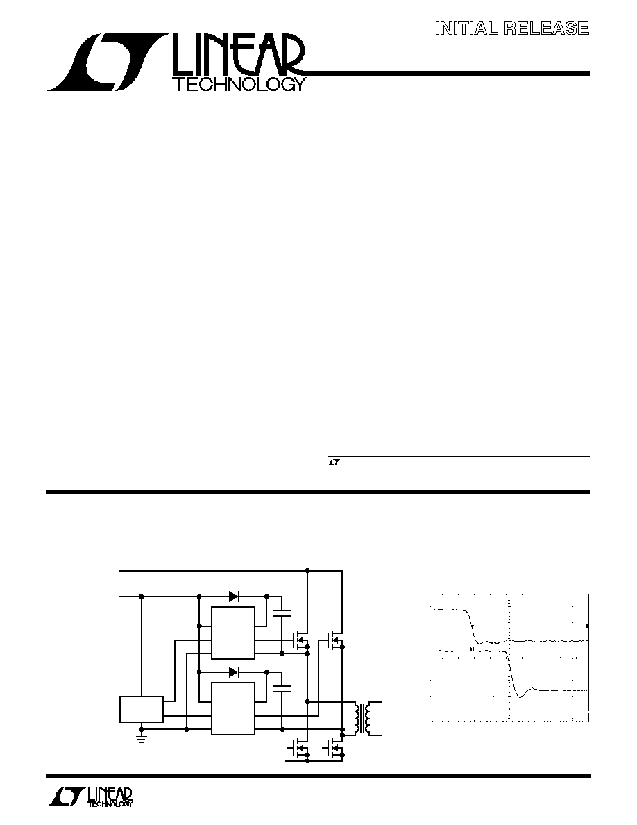
TYPICAL APPLICATIO
U
V
CC
INP
GND
BOOST
TG
TS
LTC4440
V
IN
36V TO 72V
100V PEAK TRANSIENT
(ABS MAX)
V
CC
8V TO 15V
V
CC
INP
GND
BOOST
TG
TS
LTC4440
V
CC
LTC3722-1
·
·
4440 TA01
Synchronous Phase-Modulated Full-Bridge Converter
ThinSOT is a trademark of Linear Technology Corporation.
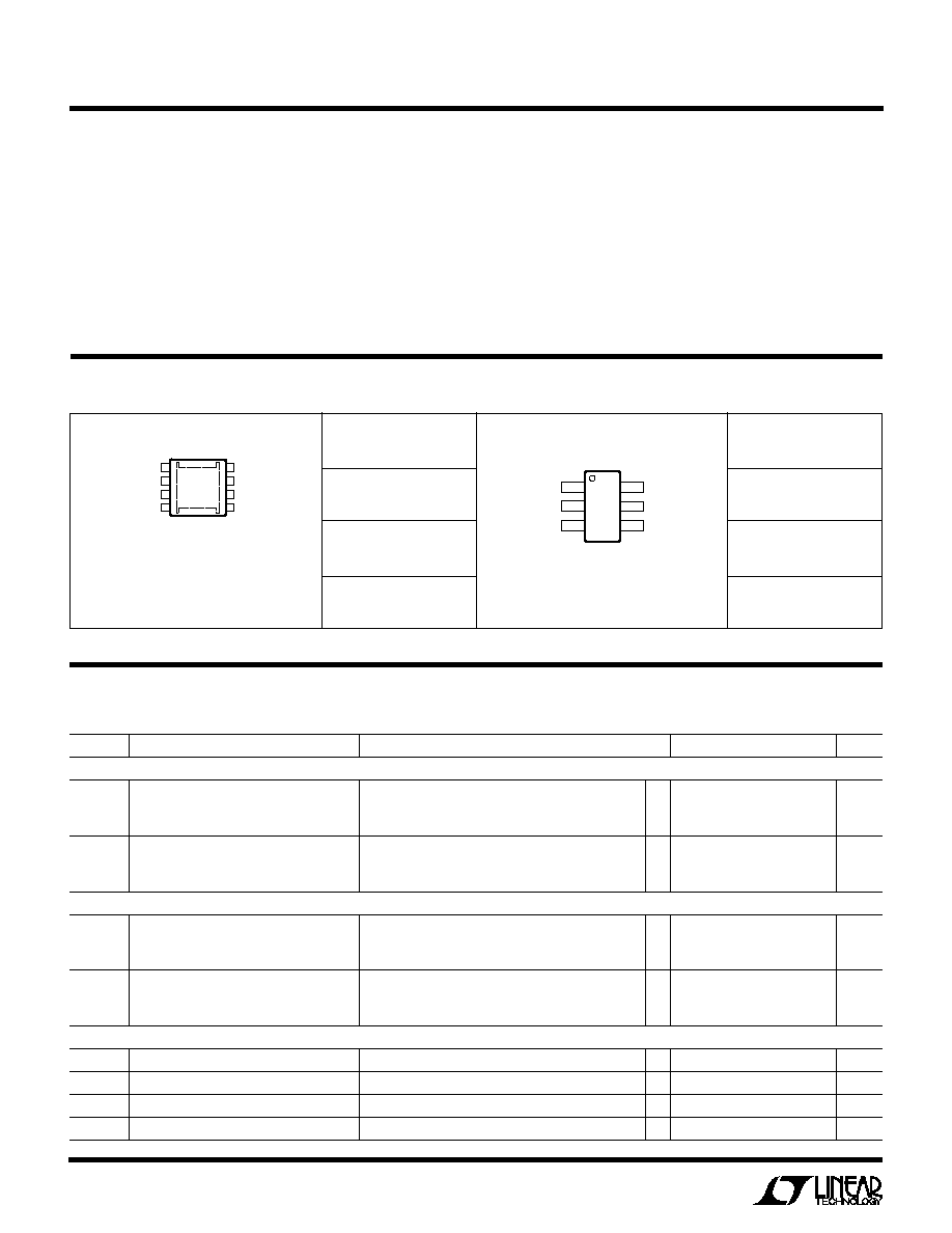
INPUT
(INP)
2V/DIV
OUTPUT
(TG TS)
5V/DIV
10ns/DIV
4440 F02
LTC4440 Driving a 1000pF
Capacitive Load
2
LTC4440
4440i
Supply Voltage
V
CC
....................................................... 0.3V to 15V
BOOST TS ......................................... 0.3V to 15V
INP Voltage ............................................... 0.3V to 15V
BOOST Voltage (Continuous) ................... 0.3V to 95V
BOOST Voltage (100ms) ........................ 0.3V to 115V
TS Voltage (Continuous) ............................. 5V to 80V
TS Voltage (100ms) ................................... 5V to 100V
ORDER PART
NUMBER
LTC4440EMS8E
T
JMAX
= 150
°
C,
JA
= 40
°
C/W (NOTE 4)
EXPOSED PAD IS GND (PIN 9)
MUST BE SOLDERED TO PCB
ABSOLUTE
M
AXI
M
U
M
RATINGS
W
W
W
U
PACKAGE/ORDER I
N
FOR
M
ATIO
N
W
U
U
(Note 1)
Peak Output Current < 1
µ
s (TG) ............................... 4A
Driver Output TG (with Respect to TS) ..... 0.3V to 15V
Operating Ambient Temperature Range
(Note 2) .............................................. 40
°
C to 85
°
C
Junction Temperature (Note 3) ............................ 150
°
C
Storage Ambient Temperature Range ... 65
°
C to 150
°
C
Lead Temperature (Soldering, 10 sec).................. 300
°
C
MS8E
PART MARKING
LTF9
1
2
3
4
INP
GND
V
CC
GND
8
7
6
5
TS
TG
BOOST
NC
TOP VIEW
9
MS8E PACKAGE
8-LEAD PLASTIC MSOP
ORDER PART
NUMBER
LTC4440ES6
S6
PART MARKING
LTZY
V
CC
1
GND 2
INP 3
6 BOOST
5 TG
4 TS
TOP VIEW
S6 PACKAGE
6-LEAD PLASTIC SOT-23
T
JMAX
= 150
°
C,
JA
= 230
°
C/W
The
q
denotes specifications which apply over the full operating
temperature range, otherwise specifications are at T
A
= 25
°
C. V
CC
= V
BOOST
= 12V, V
TS
= GND = 0V, unless otherwise noted.
Consult LTC Marketing for parts specified with wider operating temperature ranges.
ELECTRICAL CHARACTERISTICS
SYMBOL
PARAMETER
CONDITIONS
MIN
TYP
MAX
UNITS
Main Supply (V
CC
)
I
VCC
DC Supply Current
Normal Operation
INP = 0V
250
400
µ
A
UVLO
V
IN
< UVLO Threshold 0.1V
25
80
µ
A
UVLO
Undervoltage Lockout Threshold
V
CC
Rising
q
5.7
6.5
7.3
V
V
CC
Falling
q
5.4
6.2
7.0
V
Hysteresis
300
mV
Bootstrapped Supply (BOOST TS)
I
BOOST
DC Supply Current
Normal Operation
INP = 0V
110
180
µ
A
UVLO
V
BOOST
V
TS
< UVLO
HS
0.1V, INP = 0V
86
170
µ
A
UVLO
HS
Undervoltage Lockout Threshold
V
BOOST
V
TS
Rising
q
6.75
7.4
7.95
V
V
BOOST
V
TS
Falling
q
6.25
6.9
7.60
V
Hysteresis
500
mV
Input Signal (INP)
V
IH
High Input Threshold
INP Ramping High
q
1.3
1.6
2
V
V
IL
Low Input Threshold
INP Ramping Low
q
0.85
1.25
1.6
V
V
IH
V
IL
Input Voltage Hysteresis
0.350
V
I
INP
Input Pin Bias Current
±
0.01
±
2
µ
A
3
LTC4440
4440i
The
q
denotes specifications which apply over the full operating
temperature range, otherwise specifications are at T
A
= 25
°
C. V
CC
= V
BOOST
= 12V, V
TS
= GND = 0V, unless otherwise noted.
ELECTRICAL CHARACTERISTICS
Note 1: Absolute Maximum Ratings are those values beyond which the life
of a device may be impaired.
Note 2: The LTC4440 is guaranteed to meet performance specifications
from 0
°
C to 70
°
C. Specifications over the 40
°
C to 85
°
C operating
temperature range are assured by design, characterization and correlation
with statistical process controls.
Note 3: T
J
is calculated from the ambient temperature T
A
and power
dissipation PD according to the following formula:
T
J
= T
A
+ (PD ·
JA
°
C/W)
Note 4: Failure to solder the exposed back side of the MS8E package to
the PC board will result in a thermal resistance much higher than 40
°
C/W.
SYMBOL
PARAMETER
CONDITIONS
MIN
TYP
MAX
UNITS
Output Gate Driver (TG)
V
OH
High Output Voltage
I
TG
= 10mA, V
OH
= V
BOOST
V
TG
0.7
V
V
OL
Low Output Voltage
I
TG
= 100mA
q
150
220
mV
I
PU
Peak Pull-Up Current
q
1.7
2.4
A
R
DS
Output Pull-Down Resistance
q
1.5
2.2
Switching Timing
t
r
Output Rise Time
10% 90%, C
L
= 1nF
10
ns
10% 90%, C
L
= 10nF
100
ns
t
f
Output Fall Time
10% 90%, C
L
= 1nF
7
ns
10% 90%, C
L
= 10nF
70
ns
t
PLH
Output Low-High Propagation Delay
q
30
65
ns
t
PHL
Output High-Low Propagation Delay
q
28
65
ns
TYPICAL PERFOR A CE CHARACTERISTICS
U
W
V
CC
Supply Quiescent Current
vs Voltage
V
CC
SUPPLY VOLTAGE (V)
0
0
QUIESCENT CURRENT (
µ
A)
50
100
150
200
300
5
10
4440 G01
15
250
INP = V
CC
INP = 0V
T
A
= 25
°
C
BOOST TS SUPPLY VOLTAGE (V)
0
0
QUIESCENT CURRENT (
µ
A)
100
150
200
250
300
350
5
10
4440 G02
400
450
INP = 0V
500
50
15
INP = V
CC
T
A
= 25
°
C
BOOST TS SUPPLY VOLTAGE (V)
8
OUTPUT (TG TS) VOLTAGE (mV)
150
155
160
11
13
4440 G03
145
140
9
10
12
14
15
135
130
I
TG
= 100mA
T
A
= 25
°
C
BOOST TS
Supply Quiescent
Current vs Voltage
Output Low Voltage (V
OL
)
vs Supply Voltage
4
LTC4440
4440i
Output High Voltage (V
OH
)
vs Supply Voltage
BOOST TS SUPPLY VOLTAGE (V)
8
OUTPUT VOLTAGE (TG TS) (V)
14
11
4440 G04
11
9
9
10
12
8
7
15
13
12
10
13
14
15
I
TG
= 100mA
I
TG
= 1mA
I
TG
= 10mA
T
A
= 25
°
C
Input Thresholds (INP)
vs Supply Voltage
V
CC
SUPPLY VOLTAGE (V)
7
0.8
INPUT THRESHOLD (V)
1.0
1.2
1.4
1.6
1.8
2.0
9
11
13
15
4440 G05
V
IL
(INPUT LOW THRESHOLD)
V
IH
(INPUT HIGH THRESHOLD)
T
A
= 25
°
C
V
CC
Supply Current
at TTL Input Levels
2MHz Operation
V
CC
SUPPLY VOLTAGE (V)
8
V
CC
SUPPLY QUIESCENT CURRENT (
µ
A)
300
320
340
4440 G06
280
260
200
10
12
14
240
220
380
INP = 2V
INP = 0.8V
360
T
A
= 25
°
C
INPUT
(INP)
5V/DIV
OUTPUT
(TG)
5V/DIV
V
CC
= 12V
250ns/DIV
4440 G07
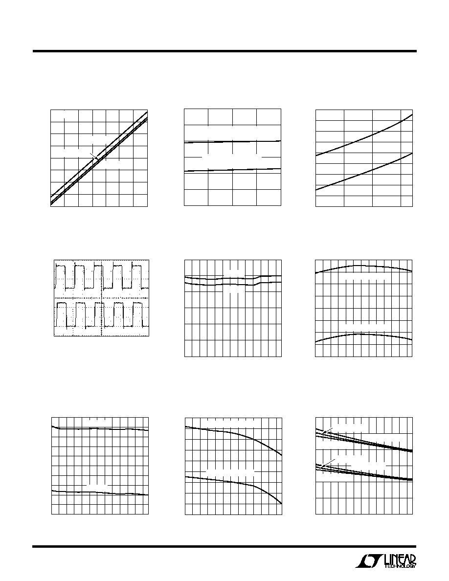
TYPICAL PERFOR A CE CHARACTERISTICS
U
W
V
CC
Supply Current (V
CC
= 12V)
vs Temperature
TEMPERATURE (
°
C)
60
CURRENT (
µ
A)
200
250
300
120
90
4440 G08
150
100
0
30
30
0
60
50
INP = 0V
INP = 12V
V
CC
Undervoltage Lockout
Thresholds vs Temperature
TEMPERATURE (
°
C)
60
V
CC
SUPPLY VOLTAGE (V)
6.45
6.40
6.35
6.30
6.25
6.20
6.15
6.10
120
90
4440 G09
6.05
30
30
0
60
FALLING THRESHOLD
RISING THRESHOLD
Boost Supply Current
vs Temperature
Boost Supply (BOOST TS)
Undervoltage Lockout Thresholds
vs Temperature
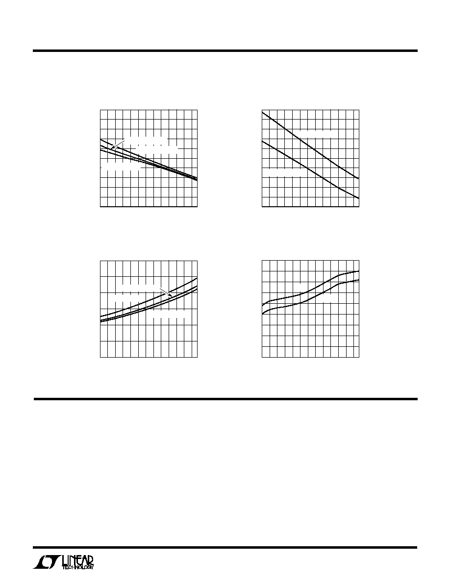
Input Threshold vs Temperature
TEMPERATURE (
°
C)
60
CURRENT (
µ
A)
500
400
450
350
300
250
200
150
100
50
120
90
4440 G10
0
30
30
0
60
INP = 0V
INP = 12V
TEMPERATURE (
°
C)
60
BOOST TS SUPPLY VOLTAGE (V)
7.6
7.5
7.4
7.3
7.2
7.1
7.0
6.9
6.8
120
90
4440 G11
6.7
30
30
0
60
FALLING THRESHOLD
RISING THRESHOLD
TEMPERATURE (
°
C)
60
INPUT THRESHOLD (V)
1.6
1.8
2.0
120
90
4440 G12
1.4
1.2
0.8
30
30
0
60
1.0
V
IH
(V
CC
= 15V)
V
IL
(V
CC
= 15V)
V
IH
(V
CC
= 8V)
V
IL
(V
CC
= 8V)
V
IH
(V
CC
= 12V)
V
IL
(V
CC
= 12V)
5
LTC4440
4440i
U
U
U
PI FU CTIO S
SOT-23 Package
V
CC
(Pin 1): Chip Supply. This pin powers the internal low
side circuitry. A low ESR ceramic bypass capacitor should
be tied between this pin and the GND pin (Pin 2).
GND (Pin 2): Chip Ground.
INP (Pin 3): Input Signal. TTL/CMOS compatible input
referenced to GND (Pin 2).
TS (Pin 4): Top (High Side) Source Connection.
Input Threshold Hysteresis
vs Temperature
Peak Driver (TG) Pull-Up Current
vs Temperature
TYPICAL PERFOR A CE CHARACTERISTICS
U
W
Output Driver Pull-Down
Resistance vs Temperature
Propagation Delay vs Temperature
(V
CC
= BOOST = 12V)
TEMPERATURE (
°
C)
60
HYSTERESIS (mV)
500
460
480
440
420
400
380
360
340
320
120
90
4440 G13
300
30
30
0
60
V
IH
-V
IL
(V
CC
= 12V)
V
IH
-V
IL
(V
CC
= 15V)
V
IH
-V
IL
(V
CC
= 8V)
TEMPERATURE (
°
C)
60
PEAK CURRENT (A)
3.0
2.8
2.9
2.7
2.6
2.5
2.4
2.3
2.2
2.1
120
90
4440 G14
2.0
30
30
0
60
BOOST TS = 12V
BOOST TS = 15V
TG (Pin 5): High Current Gate Driver Output (Top Gate).
This pin swings between TS and BOOST 0.7V.
BOOST (Pin 6): High Side Bootstrapped Supply. An exter-
nal capacitor should be tied between this pin and TS
(Pin 4). Normally, a bootstrap diode is connected between
V
CC
(Pin 1) and this pin. Voltage swing at this pin is from
V
CC
V
D
to V
IN
+ V
CC
V
D
, where V
D
is the forward voltage
drop of the bootstrap diode.
TEMPERATURE (
°
C)
60
R
DS
(
)
2.0
2.5
3.0
120
90
4440 G15
1.5
1.0
0
30
30
0
60
0.5
BOOST TS = 15V
BOOST TS = 8V
BOOST TS = 12V
TEMPERATURE (
°
C)
60
PROPAGATION DELAY (ns)
45
40
35
30
25
20
15
10
5
120
90
4440 G16
0
30
30
0
60
t
PLH
t
PHL