 | –≠–ª–µ–∫—Ç—Ä–æ–Ω–Ω—ã–π –∫–æ–º–ø–æ–Ω–µ–Ω—Ç: LTC6800 | –°–∫–∞—á–∞—Ç—å:  PDF PDF  ZIP ZIP |
LTC6800
1
6800fa
The LTC
Æ
6800 is a precision instrumentation amplifier.
The CMRR is typically 116dB with a single 5V supply and
is independent of gain. The input offset voltage is guaran-
teed below 100
µ
V with a temperature drift of less than
250nV/
∞
C. The LTC6800 is easy to use; the gain is adjust-
able with two external resistors, like a traditional op amp.
The LTC6800 uses charge balanced sampled data tech-
niques to convert a differential input voltage into a single
ended signal that is in turn amplified by a zero-drift
operational amplifier.
The differential inputs operate from rail-to-rail and the
single ended output swings from rail-to-rail. The LTC6800
is available in an MS8 surface mount package. For space
limited applications, the LTC6800 is available in a
3mm
◊
3mm
◊
0.8mm dual fine pitch leadless package
(DFN).
s
Thermocouple Amplifiers
s
Electronic Scales
s
Medical Instrumentation
s
Strain Gauge Amplifiers
s
High Resolution Data Acquisition
s
116dB CMRR Independent of Gain
s
Maximum Offset Voltage: 100
µ
V
s
Maximum Offset Voltage Drift: 250nV/
∞
C
s
≠ 40
∞
C to 125
∞
C Operation
s
Rail-to-Rail Input Range
s
Rail-to-Rail Output Swing
s
Supply Operation: 2.7V to 5.5V
s
Available in an MS8 and 3mm
◊
3mm
◊
0.8mm
DFN Packages
Rail-to-Rail
Input and Output,
Instrumentation Amplifier
, LTC and LT are registered trademarks of Linear Technology Corporation.
≠
+
LTC6800
4
5
6
7
OUT
100mV/A
OF LOAD
CURRENT
10k
1.5m
0.1
µ
F
150
6800 TA01
I
LOAD
8
2
V
REGULATOR
3
LOAD
INPUT COMMON MODE VOLTAGE (V)
0
≠15
V
OS
(
µ
V)
≠10
≠5
0
5
15
0.5
1
1.5
2
6800 TA02
2.5
3
10
V
S
= 3V
V
REF
= 0V
T
A
= 25
∞
C
G = 1000
G = 100
G = 10
G = 1
High Side Power Supply Current Sense
Typical Input Referred Offset vs
Input Common Mode Voltage (V
S
= 3V)
DESCRIPTIO
U
FEATURES
APPLICATIO S
U
TYPICAL APPLICATIO
U
LTC6800
2
6800fa
TOP VIEW
DD PACKAGE
8-LEAD (3mm
◊
3mm) PLASTIC DFN
5
6
7
8
4
3
2
1
NC
≠IN
+IN
V
≠
V
+
OUT
RG
REF
Total Supply Voltage (V
+
to V
≠
) .............................. 5.5V
Input Current ......................................................
±
10mA
V
IN
+
≠ V
REF
........................................................
5.5V
V
IN
≠
≠ V
REF
........................................................
5.5V
Output Short Circuit Duration .......................... Indefinite
ABSOLUTE AXI U
RATI GS
W
W
W
U
(Note 1)
1
2
3
4
NC
≠IN
+IN
V
≠
8
7
6
5
V
+
OUT
RG
REF
TOP VIEW
MS8 PACKAGE
8-LEAD PLASTIC MSOP
PACKAGE/ORDER I FOR ATIO
U
U
W
ORDER PART NUMBER
DD PART MARKING
T
JMAX
= 125
∞
C,
JA
= 160
∞
C/W
UNDERSIDE METAL INTERNALLY
CONNECTED TO V
≠
(PCB CONNECTION OPTIONAL)
LAEP
LTC6800HDD
Consult LTC Marketing for parts specified with wider operating temperature ranges.
ORDER PART NUMBER
MS8 PART MARKING
T
JMAX
= 150
∞
C,
JA
= 200
∞
C/W
LTADE
LTC6800HMS8
Operating Temperature Range
(Note 7) ................................................ ≠ 40
∞
C to 125
∞
C
Storage Temperature Range
MS8 Package ................................... ≠ 65
∞
C to 150
∞
C
DD Package ...................................... ≠ 65
∞
C to 125
∞
C
Lead Temperature (Soldering, 10 sec).................. 300
∞
C
ELECTRICAL CHARACTERISTICS
The
q
denotes the specifications which apply over the full operating
temperature range, otherwise specifications are at T
A
= 25
∞
C. V
+
= 3V, V
≠
= 0V, REF = 200mV. Output voltage swing is referenced
to V
≠
. All other specifications reference the OUT pin to the REF pin.
PARAMETER
CONDITIONS
MIN
TYP
MAX
UNITS
Input Offset Voltage (Note 2)
V
CM
= 200mV
±
100
µ
V
Average Input Offset Drift (Note 2)
T
A
= ≠40
∞
C to 85
∞
C
q
±
250
nV/
∞
C
T
A
= 85
∞
C to 125
∞
C
q
≠1
≠2.5
µ
V/
∞
C
Common Mode Rejection Ratio
A
V
= 1, V
CM
= 0V to 3V
q
90
113
dB
(Notes 4, 5)
Integrated Input Bias Current (Note 3)
V
CM
= 1.2V
4
10
nA
Integrated Input Offset Current (Note 3)
V
CM
= 1.2V
1
3
nA
Input Noise Voltage
DC to 10Hz
2.5
µ
V
P-P
Power Supply Rejection Ratio (Note 6)
V
S
= 2.7V to 5.5V
q
110
116
dB
Output Voltage Swing High
R
L
= 2k to V
≠
q
2.85
2.94
V
R
L
= 10k to V
≠
q
2.95
2.98
V
Output Voltage Swing Low
q
20
mV
Gain Error
A
V
= 1
0.1
%
Gain Nonlinearity
A
V
= 1
100
ppm
LTC6800
3
6800fa
Supply Current
No Load
q
1.2
mA
Internal Op Amp Gain Bandwidth
200
kHz
Slew Rate
0.2
V/
µ
s
Internal Sampling Frequency
3
kHz
The
q
denotes the specifications which apply over the full operating
temperature range, otherwise specifications are at T
A
= 25
∞
C. V
+
= 3V, V
≠
= 0V, REF = 200mV. Output voltage swing is referenced
to V
≠
. All other specifications reference the OUT pin to the REF pin.
PARAMETER
CONDITIONS
MIN
TYP
MAX
UNITS
Note 1: Absolute Maximum Ratings are those values beyond which the life
of a device may be impaired.
Note 2: These parameters are guaranteed by design. Thermocouple effects
preclude measurement of these voltage levels in high speed automatic test
systems. V
OS
is measured to a limit determined by test equipment
capability.
Note 3: If the total source resistance is less than 10k, no DC errors result
from the input bias currents or the mismatch of the input bias currents or
the mismatch of the resistances connected to ≠IN and +IN.
Note 4: The CMRR with a voltage gain, A
V
, larger than 10 is 120dB (typ).
Note 5: At temperatures above 70
∞
C, the common mode rejection ratio
lowers when the common mode input voltage is within 100mV of the
supply rails.
Note 6: The power supply rejection ratio (PSRR) measurement accuracy
depends on the proximity of the power supply bypass capacitor to the
device under test. Because of this, the PSRR is 100% tested to relaxed
limits at final test. However, their values are guaranteed by design to meet
the data sheet limits.
Note 7: The LTC6800H is guaranteed functional over the operating
temperature range of ≠40
∞
C to 125
∞
C. Specifications over the ≠40
∞
C to
125
∞
C range (denoted by
q
) are assured by design and characterization
but are not tested or QA sampled at these temperatures.
ELECTRICAL CHARACTERISTICS
The
q
denotes the specifications which apply over the full operating temperature range, otherwise specifications are at T
A
= 25
∞
C. V
+
= 5V,
V
≠
= 0V, REF = 200mV. Output voltage swing is referenced to V
≠
. All other specifications reference the OUT pin to the REF pin.
PARAMETER
CONDITIONS
MIN
TYP
MAX
UNITS
Input Offset Voltage (Note 2)
V
CM
= 200mV
±
100
µ
V
Average Input Offset Drift (Note 2)
T
A
= ≠40
∞
C to 85
∞
C
q
±
250
nV/
∞
C
T
A
= 85
∞
C to 125
∞
C
q
≠1
≠2.5
µ
V/
∞
C
Common Mode Rejection Ratio
A
V
= 1, V
CM
= 0V to 5V
q
90
116
dB
(Notes 4, 5)
Integrated Input Bias Current (Note 3)
V
CM
= 1.2V
4
10
nA
Integrated Input Offset Current (Note 3)
V
CM
= 1.2V
1
3
nA
Power Supply Rejection Ratio (Note 6)
V
S
= 2.7V to 5.5V
q
110
116
dB
Output Voltage Swing High
R
L
= 2k to V
≠
q
4.85
4.94
V
R
L
= 10k to V
≠
q
4.95
4.98
V
Output Voltage Swing Low
q
20
mV
Gain Error
A
V
= 1
0.1
%
Gain Nonlinearity
A
V
= 1
100
ppm
Supply Current
No Load
q
1.3
mA
Internal Op Amp Gain Bandwidth
200
kHz
Slew Rate
0.2
V/
µ
s
Internal Sampling Frequency
3
kHz
LTC6800
4
6800fa
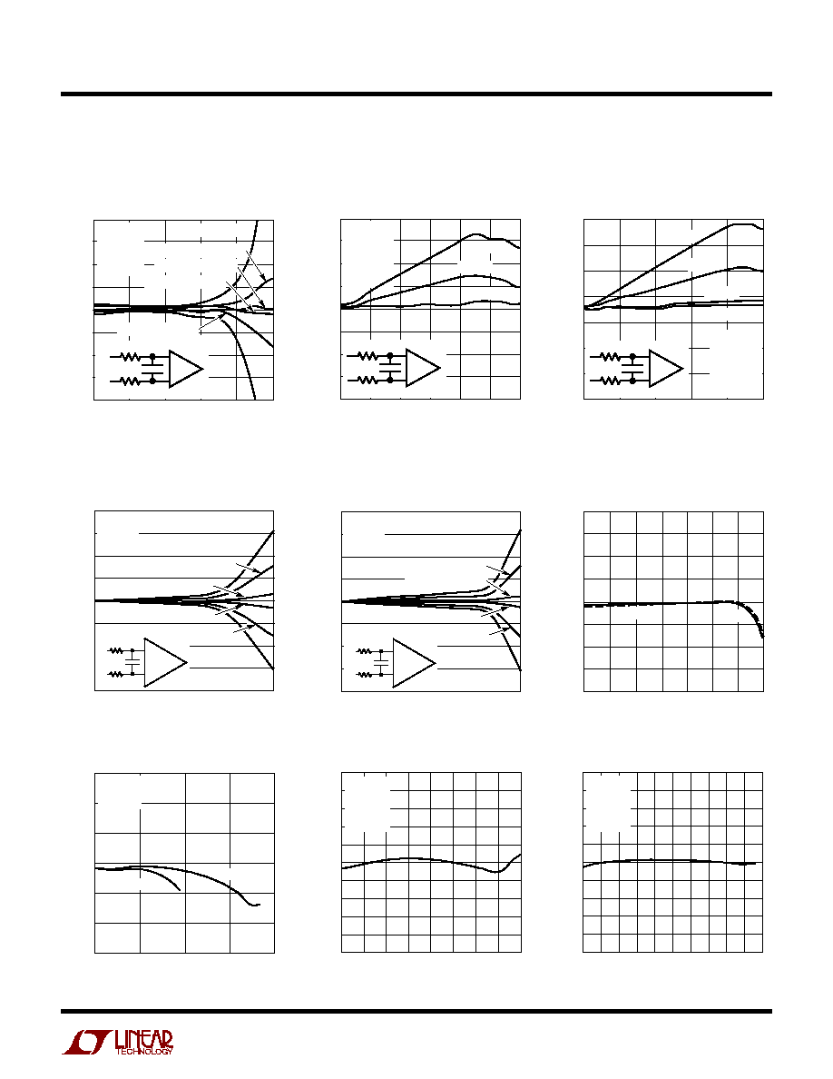
TYPICAL PERFOR A CE CHARACTERISTICS
U
W
Input Offset Voltage
vs Input Common Mode Voltage
INPUT COMMON MODE VOLTAGE (V)
0
INPUT OFFSET VOLTAGE (
µ
V)
15
10
5
0
≠5
≠10
≠15
0.5
1.0
1.5
2.0
6800 G01
2.5
3.0
V
S
= 3V
V
REF
= 0V
T
A
= 25
∞
C
G = 1000
G = 100
G = 10
G = 1
Input Offset Voltage
vs Input Common Mode Voltage
Input Offset Voltage
vs Input Common Mode Voltage
INPUT COMMON MODE VOLTAGE (V)
0
INPUT OFFSET VOLTAGE (
µ
V)
15
10
5
0
≠5
≠10
≠15
1
2
3
4
2053 G02
5
V
S
= 5V
V
REF
= 0V
T
A
= 25
∞
C
G = 1000
G = 100
G = 1
G = 10
INPUT COMMON MODE VOLTAGE (V)
INPUT OFFSET VOLTAGE (
µ
V)
20
15
10
5
0
≠5
≠10
≠15
≠20
6800 G03
0
0.5
1.0
1.5
2.0
2.5
3.0
V
S
= 3V
V
REF
= 0V
G = 10
T
A
= 25
∞
C
T
A
= 70
∞
C
T
A
= ≠55
∞
C
Input Offset Voltage
vs Input Common Mode Voltage
INPUT COMMON MODE VOLTAGE (V)
0
INPUT OFFSET VOLTAGE (
µ
V)
20
15
10
5
0
≠5
≠10
≠15
≠20
1
2
3
4
6800 G04
5
V
S
= 5V
V
REF
= 0V
G = 10
T
A
= 25
∞
C
T
A
= ≠55
∞
C
T
A
= 70
∞
C
Input Offset Voltage vs Input
Common Mode Voltage,
85
∞
C
T
A
125
∞
C
Input Offset Voltage vs Input
Common Mode Voltage,
85
∞
C
T
A
125
∞
C
INPUT COMMON MODE VOLTAGE (V)
INPUT OFFSET VOLTAGE (
µ
V)
60
40
20
0
≠20
≠40
≠60
6800 G05
0
0.5
1.0
1.5
2.0
2.5
3.0
V
S
= 3V
V
REF
= 0V
G = 10
T
A
= 85
∞
C
T
A
= 125
∞
C
INPUT COMMON MODE VOLTAGE (V)
0
INPUT OFFSET VOLTAGE (
µ
V)
60
40
20
0
≠20
≠40
≠60
6800 G06
0
1
2
3
4
5
V
S
= 5V
V
REF
= 0V
G = 10
T
A
= 85
∞
C
T
A
= 125
∞
C
Additional Input Offset Due to
Input R
S
vs Input Common Mode
(C
IN
< 100pF)
INPUT COMMON MODE VOLTAGE (V)
0
ADDITIONAL OFFSET ERROR (
µ
V)
60
40
20
0
≠20
≠40
≠60
0.5
1.0
1.5
2.0
6800 G07
2.5
3.0
V
S
= 3V
V
REF
= 0V
R
+
= R
≠
= R
S
C
IN
< 100pF
G = 10
T
A
= 25
∞
C
R
S
= 0k
R
S
= 20k
R
S
= 10k
R
S
= 5k
+
≠
R
S
R
S
SMALL C
IN
R
S
= 15k
Additional Input Offset Due to
Input R
S
vs Input Common Mode
(C
IN
< 100pF)
Additional Input Offset Due to Input
R
S
Mismatch vs Input Common
Mode (C
IN
< 100pF)
INPUT COMMON MODE VOLTAGE (V)
0
ADDITIONAL OFFSET ERROR (
µ
V)
30
20
10
0
≠10
≠20
≠30
1
2
3
4
6800 G08
5
V
S
= 5V
V
REF
= 0V
R
IN
+
= R
IN
≠
= R
S
C
IN
< 100pF
G = 10
T
A
= 25
∞
C
R
S
= 20k
R
S
= 15k
R
S
= 10k
R
S
= 5k
+
≠
R
S
R
S
SMALL C
IN
INPUT COMMON MODE VOLTAGE (V)
0
ADDITIONAL OFFSET ERROR (
µ
V)
0.5
1.0
1.5
2.0
6800 G09
2.5
3.0
50
40
30
20
10
0
≠10
≠20
≠30
≠40
≠50
V
S
= 3V
V
REF
= 0V
C
IN
< 100pF
G = 10
T
A
= 25
∞
C
R
+
= 0k, R
≠
= 10k
R
+
= 0k, R
≠
= 15k
R
+
= 0k, R
≠
= 5k
+
≠
R
+
R
≠
SMALL C
IN
R
+
=15k, R
≠
= 0k
R
+
= 5k, R
≠
= 0k
R
+
= 10k, R
≠
= 0k
LTC6800
5
6800fa
TYPICAL PERFOR A CE CHARACTERISTICS
U
W
Additional Input Offset Due to Input
R
S
Mismatch vs Input Common
Mode (C
IN
< 100pF)
Additional Input Offset Due to
Input R
S
vs Input Common Mode
(C
IN
> 1
µ
F)
Additional Input Offset Due to
Input R
S
vs Input Common Mode
(C
IN
> 1
µ
F)
INPUT COMMON MODE VOLTAGE (V)
0
ADDITIONAL OFFSET ERROR (
µ
V)
1
2
3
4
6800 G10
5
40
30
20
10
0
≠10
≠20
≠30
≠40
V
S
= 5V
V
REF
= 0V
C
IN
< 100pF
G = 10
T
A
= 25
∞
C
R
IN
+
= 0k, R
IN
≠
= 20k
R
IN
+
= 0k, R
IN
≠
= 15k
R
IN
+
= 0k, R
IN
≠
= 10k
R
IN
+
= 10k, R
IN
≠
= 0k
+
≠
R
+
R
≠
SMALL C
IN
R
IN
+
= 15k, R
IN
≠
= 0k
R
IN
+
= 20k, R
IN
≠
= 0k
INPUT COMMON MODE VOLTAGE (V)
0
ADDITIONAL OFFSET ERROR (
µ
V)
0.5
1.0
1.5
2.0
6800 G11
2.5
3.0
40
30
20
10
0
≠10
≠20
≠30
≠40
V
S
= 3V
V
REF
= 0V
R
+
= R
≠
= R
S
C
IN
> 1
µ
F
G = 10
T
A
= 25
∞
C
R
S
= 15k
R
S
= 10k
R
S
= 5k
+
≠
R
S
R
S
BIG C
IN
INPUT COMMON MODE VOLTAGE (V)
0
ADDITIONAL OFFSET ERROR (
µ
V)
70
50
30
10
≠10
≠30
≠50
≠70
1
2
3
4
6800 G12
5
V
S
= 5V
V
REF
= 0V
R
+
= R
≠
= R
S
C
IN
> 1
µ
F
G = 10
T
A
= 25
∞
C
R
S
= 500
R
S
= 10k
R
S
= 1k
R
S
= 5k
+
≠
R
S
R
S
BIG C
IN
Additional Input Offset Due to
Input R
S
Mismatch vs Input
Common Mode (C
IN
> 1
µ
F)
Offset Voltage vs Temperature
INPUT COMMON MODE VOLTAGE (V)
ADDITIONAL OFFSET ERROR (
µ
V)
6800 G13
200
150
100
50
0
≠50
≠100
≠150
≠200
0
0.5
R
+
= 0
, R
≠
= 1k
R
+
= 1k, R
≠
= 0
R
+
= 100
, R
≠
= 0
R
+
= 0
, R
≠
= 500
1.0
1.5
2.0
2.5
3.0
V
S
= 3V
V
REF
= 0V
T
A
= 25
∞
C
G = 10
R
+
= 0
, R
≠
= 100
≠
+
C
IN
BIG
R
+
R
≠
R
+
= 500
, R
≠
= 0
INPUT COMMON MODE VOLTAGE (V)
0
ADDITIONAL OFFSET ERROR (
µ
V)
≠50
0
50
3
5
6800 G14
≠100
≠150
≠200
1
2
4
100
150
200
R
+
= 0
, R
≠
= 100
R
+
= 0
, R
≠
= 500
R
+
= 0
, R
≠
= 1k
R
+
= 100
, R
≠
= 0
R
+
= 1k, R
≠
= 0
V
S
= 5V
V
REF
= 0V
T
A
= 25
∞
C
G = 10
≠
+
C
IN
BIG
R
+
R
≠
R
+
= 500
, R
≠
= 0
≠50
INPUT OFFSET VOLTAGE (
µ
V)
80
60
40
20
0
≠20
≠40
≠60
≠80
TEMPERATURE (
∞
C)
100
6800 G15
0
50
≠25
25
75
125
V
S
= 3V
V
S
= 5V
V
OS
vs V
REF
V
REF
(V)
0
V
OS
(
µ
V)
30
20
10
0
≠10
≠20
≠30
6800 G16
1
2
3
4
V
S
= 3V
V
S
= 5V
V
IN
+
= V
IN
≠
= REF
G = 10
T
A
= 25
∞
C
OUTPUT VOLTAGE (V)
≠2.4
NONLINEARITY (ppm)
10
8
6
4
2
0
≠2
≠4
≠6
≠8
≠10
≠1.4
≠0.4
0.1
6800 G17
≠1.9
≠0.9
0.6
1.1
1.6
V
S
=
±
2.5V
V
REF
= 0V
G = 1
R
L
= 10k
T
A
= 25
∞
C
OUTPUT VOLTAGE (V)
≠2.4
NONLINEARITY (ppm)
10
8
6
4
2
0
≠2
≠4
≠6
≠8
≠10
≠1.4
≠0.4
6800 G18
0.6
1.6
2.6
V
S
=
±
2.5V
V
REF
= 0V
G = 10
R
L
= 10k
T
A
= 25
∞
C
Gain Nonlinearity, G = 1
Gain Nonlinearity, G = 10
Additional Input Offset Due to
Input R
S
Mismatch vs Input
Common Mode (C
IN
> 1
µ
F)
LTC6800
6
6800fa
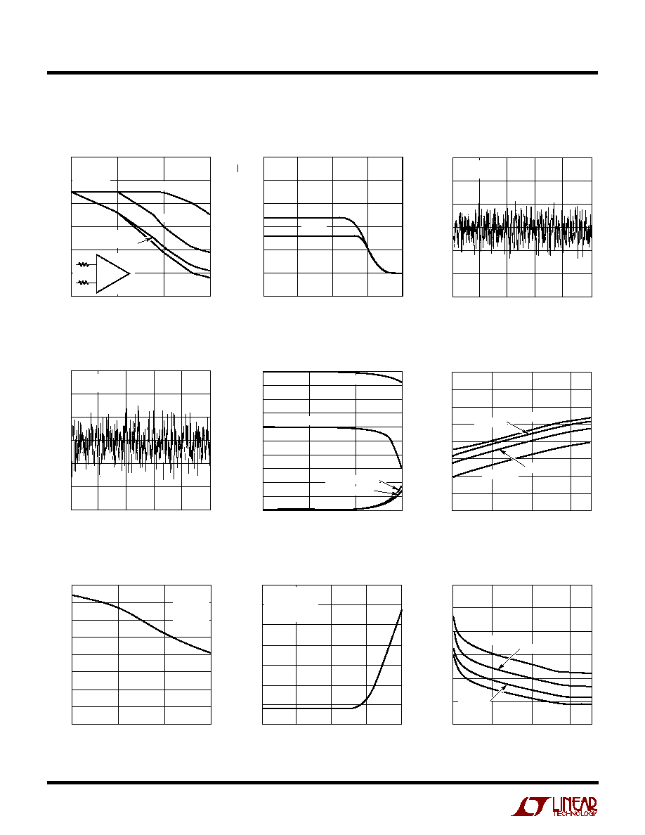
TYPICAL PERFOR A CE CHARACTERISTICS
U
W
CMRR vs Frequency
Input Voltage Noise Density
vs Frequency
FREQUENCY (Hz)
1
CMRR (db)
120
120
110
100
90
80
70
10
100
1000
6800 G19
V
S
= 3V, 5V
V
IN
= 1V
P-P
T
A
= 25
∞
C
≠
+
R
+
R
≠
R
+
= R
≠
= 1k
R
+
= R
≠
= 10k
R
+
= 10k, R
≠
= 0
R
+
= 0
, R
≠
= 10k
FREQUENCY (Hz)
1
INPUT REFERRED NOISE DENSITY (nV/
Hz)
300
250
200
150
100
50
0
10
100
1000
10000
6800 G20
G = 10
T
A
= 25
∞
C
V
S
= 5V
V
S
= 3V
Input Referred Noise in 10Hz
Bandwidth
TIME (s)
≠5
INPUT REFFERED NOISE VOLTAGE (
µ
V)
3
2
1
0
≠1
≠2
≠3
≠3
≠1
1
3
6800 G21
5
V
S
= 3V
T
A
= 25
∞
C
Output Voltage Swing
vs Output Current
Supply Current vs Supply Voltage
Input Referred Noise in 10Hz
Bandwidth
TIME (s)
≠5
INPUT REFFERED NOISE VOLTAGE (
µ
V)
3
2
1
0
≠1
≠2
≠3
≠3
≠1
1
3
6800 G22
5
V
S
= 5V
T
A
= 25
∞
C
OUTPUT CURRENT (mA)
0.01
OUTPUT VOLTAGE SWING (V)
0.1
1
10
6800 G23
5.0
4.5
4.0
3.5
3.0
2.5
2.0
1.5
1.0
0.5
0
T
A
= 25
∞
C
V
S
= 5V, SOURCING
V
S
= 3V, SOURCING
V
S
= 5V, SINKING
V
S
= 3V, SINKING
SUPPLY VOLTAGE (V)
2.5
SUPPLY CURRENT (mA)
6800 G24
4.5
3.5
5.5
6
1.00
0.95
0.90
0.85
0.80
0.75
0.70
0.65
0.60
T
A
= ≠55
∞
C
T
A
= 85
∞
C
T
A
= 125
∞
C
T
A
= 0
∞
C
Settling Time vs Gain
Internal Clock Frequency
vs Supply Voltage
Low Gain Settling Time
vs Settling Accuracy
SETTLING ACCURACY (%)
0.0001
SETTLING TIME (ms)
6800 G25
0.001
0.01
0.1
8
7
6
5
4
3
2
1
0
V
S
= 5V
dV
OUT
= 1V
G < 100
T
A
= 25
∞
C
GAIN (V/V)
1
SETTLING TIME (ms)
35
30
25
20
15
10
5
0
10
100
1000
10000
6800 G26
V
S
= 5V
dV
OUT
= 1V
0.1% ACCURACY
T
A
= 25
∞
C
SUPPLY VOLTAGE (V)
2.5
CLOCK FREQUENCY (kHz)
6800 G27
4.5
5.5
6
3.5
3.40
3.35
3.30
3.25
3.20
3.15
3.10
T
A
= ≠55
∞
C
T
A
= 85
∞
C
T
A
= 125
∞
C
T
A
= 25
∞
C
LTC6800
7
6800fa
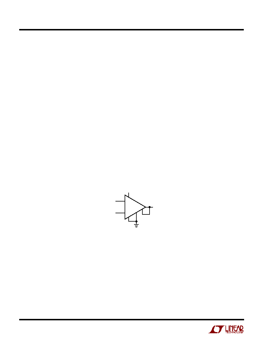
NC (Pin 1): Not Connected.
≠IN (Pin 2): Inverting Input.
+IN (Pin 3): Noninverting Input.
V
≠
(Pin 4): Negative Supply.
REF (Pin 5): Voltage Reference (V
REF
) for Amplifier Output.
PI FU CTIO S
U
U
U
RG (Pin 6): Inverting Input of Internal Op Amp. With a
resistor, R2, connected between the OUT pin and the RG
pin and a resistor, R1, between the RG pin and the REF pin,
the DC gain is given by 1 + R2 / R1.
OUT (Pin 7): Amplifier Output.
V
OUT
= GAIN (V
+IN
≠ V
≠IN
) + V
REF
V
+
(Pin 8): Positive Supply.
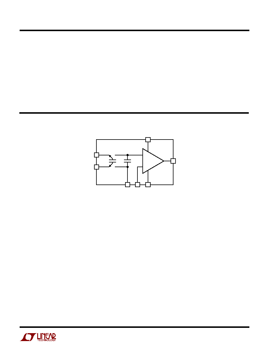
BLOCK DIAGRA
W
≠
+
C
H
OUT
6800 BD
4
V
≠
5
REF
6
RG
8
V
+
3
+IN
2
≠IN
C
S
7
LTC6800
8
6800fa
where V
+IN
and V
≠IN
are the voltages of the +IN and ≠IN
pins respectively, V
REF
is the voltage at the REF pin and V
+
is the positive supply voltage.
For example, with a 3V single supply and a 0V to 100mV
differential input voltage, V
REF
must be between 0V and
1.6V.
Settling Time
The sampling rate is 3kHz and the input sampling period
during which C
S
is charged to the input differential voltage
V
IN
is approximately 150
µ
s. First assume that on each
input sampling period, C
S
is charged fully to V
IN
. Since
C
S
= C
H
(= 1000pF), a change in the input will settle to N
bits of accuracy at the op amp noninverting input after N
clock cycles or 333
µ
s(N). The settling time at the OUT pin
is also affected by the settling of the internal op amp.
Since the gain bandwidth of the internal op amp is
typically 200kHz, the settling time is dominated by the
switched capacitor front end for gains below 100 (see
Typical Performance Characteristics).
APPLICATIO S I FOR ATIO
W
U
U
U
Theory of Operation
The LTC6800 uses an internal capacitor (C
S
) to sample a
differential input signal riding on a DC common mode
voltage (see Block Diagram). This capacitor's charge is
transferred to a second internal hold capacitor (C
H
) trans-
lating the common mode of the input differential signal to
that of the REF pin. The resulting signal is amplified by a
zero-drift op amp in the noninverting configuration. The
RG pin is the negative input of this op amp and allows
external programmability of the DC gain. Simple filtering
can be realized by using an external capacitor across the
feedback resistor.
Input Voltage Range
The input common mode voltage range of the LTC6800 is
rail-to-rail. However, the following equation limits the size
of the differential input voltage:
V
≠
(V
+IN
≠ V
≠IN
) + V
REF
V
+
≠ 1.3
≠
+
≠
+
V
D
V
+IN
V
≠IN
3
8
5V
4
5
6
7
2
6800 F01
0V < V
+IN
< 5V
0V < V
≠IN
< 5V
0V < V
D
< 3.7V
V
OUT
= V
D
SINGLE SUPPLY, UNITY GAIN
Figure 1

LTC6800
9
6800fa
APPLICATIO S I FOR ATIO
W
U
U
U
Input Current
Whenever the differential input V
IN
changes, C
H
must be
charged up to the new input voltage via C
S
. This results in
an input charging current during each input sampling
period. Eventually, C
H
and C
S
will reach V
IN
and, ideally,
the input current would go to zero for DC inputs.
In reality, there are additional parasitic capacitors which
disturb the charge on C
S
every cycle even if V
IN
is a DC
voltage. For example, the parasitic bottom plate capacitor
on C
S
must be charged from the voltage on the REF pin to
the voltage on the ≠IN pin every cycle. The resulting input
charging current decays exponentially during each input
sampling period with a time constant equal to R
S
C
S
. If the
voltage disturbance due to these currents settles before
the end of the sampling period, there will be no errors
due to source resistance or the source resistance mis-
match between ≠IN and +IN. With R
S
less than 10k, no
DC errors occur due to this input current.
In the Typical Performance Characteristics section of this
data sheet, there are curves showing the additional error
from nonzero source resistance in the inputs. If there are
no large capacitors across the inputs, the amplifier is less
sensitive to source resistance and source resistance mis-
match. When large capacitors are placed across the in-
puts, the input charging currents described above result in
larger DC errors, especially with source resistor mis-
matches.
Power Supply Bypassing
The LTC6800 uses a sampled data technique and therefore
contains some clocked digital circuitry. It is therefore sen-
sitive to supply bypassing. A 0.1
µ
F ceramic capacitor must
be connected between Pin 8 (V
+
) and Pin 4 (V
≠
) with leads
as short as possible.
LTC6800
10
6800fa
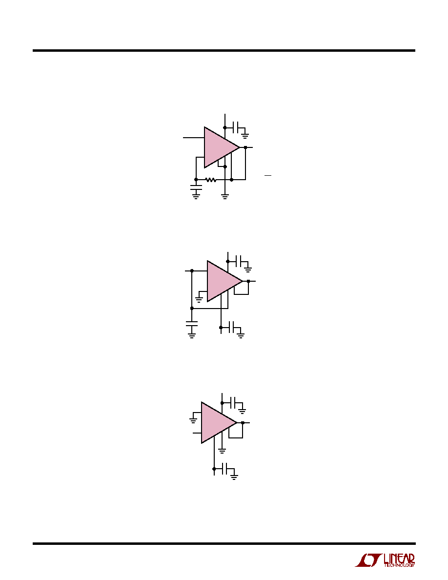
TYPICAL APPLICATIO S
U
Precision
˜
2
6800 TA03
≠
+
4
5
6
7
V
OUT
5V
LTC6800
8
3
2
0.1
µ
F
V
IN
0.1
µ
F
1k
V
OUT
=
V
IN
2
6800 TA04
≠
+
4
5
6
7
2.5V
LTC6800
8
3
2
0.1
µ
F
0.1
µ
F
0.1
µ
F
≠2.5V
V
IN
V
OUT
V
OUT
= 2V
IN
V
IN
6800 TA05
≠
+
4
5
6
7
2.5V
LTC6800
8
3
2
0.1
µ
F
0.1
µ
F
≠2.5V
V
OUT
V
OUT
= ≠V
IN
Precision Doubler (General Purpose)
Precision Inversion (General Purpose)
LTC6800
11
6800fa
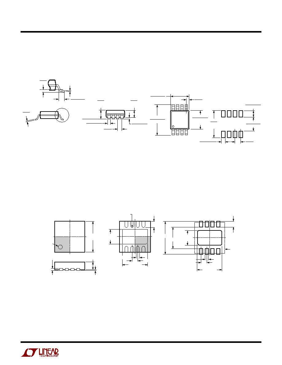
PACKAGE DESCRIPTIO
U
MS8 Package
8-Lead Plastic MSOP
(Reference LTC DWG # 05-08-1660)
MSOP (MS8) 0603
0.53
±
0.152
(.021
±
.006)
SEATING
PLANE
NOTE:
1. DIMENSIONS IN MILLIMETER/(INCH)
2. DRAWING NOT TO SCALE
3. DIMENSION DOES NOT INCLUDE MOLD FLASH, PROTRUSIONS OR GATE BURRS.
MOLD FLASH, PROTRUSIONS OR GATE BURRS SHALL NOT EXCEED 0.152mm (.006") PER SIDE
4. DIMENSION DOES NOT INCLUDE INTERLEAD FLASH OR PROTRUSIONS.
INTERLEAD FLASH OR PROTRUSIONS SHALL NOT EXCEED 0.152mm (.006") PER SIDE
5. LEAD COPLANARITY (BOTTOM OF LEADS AFTER FORMING) SHALL BE 0.102mm (.004") MAX
0.18
(.007)
0.254
(.010)
1.10
(.043)
MAX
0.22 ≠ 0.38
(.009 ≠ .015)
TYP
0.127
±
0.076
(.005
±
.003)
0.86
(.034)
REF
0.65
(.0256)
BSC
0
∞
≠ 6
∞
TYP
DETAIL "A"
DETAIL "A"
GAUGE PLANE
1
2
3
4
4.90
±
0.152
(.193
±
.006)
8
7 6 5
3.00
±
0.102
(.118
±
.004)
(NOTE 3)
3.00
±
0.102
(.118
±
.004)
(NOTE 4)
0.52
(.0205)
REF
5.23
(.206)
MIN
3.20 ≠ 3.45
(.126 ≠ .136)
0.889
±
0.127
(.035
±
.005)
RECOMMENDED SOLDER PAD LAYOUT
0.42
±
0.038
(.0165
±
.0015)
TYP
0.65
(.0256)
BSC
Information furnished by Linear Technology Corporation is believed to be accurate and reliable.
However, no responsibility is assumed for its use. Linear Technology Corporation makes no represen-
tation that the interconnection of its circuits as described herein will not infringe on existing patent rights.
3.00
±
0.10
(4 SIDES)
NOTE:
1. DRAWING TO BE MADE A JEDEC PACKAGE OUTLINE M0-229 VARIATION OF (WEED-1)
2. ALL DIMENSIONS ARE IN MILLIMETERS
3. DIMENSIONS OF EXPOSED PAD ON BOTTOM OF PACKAGE DO NOT INCLUDE
MOLD FLASH. MOLD FLASH, IF PRESENT, SHALL NOT EXCEED 0.15mm ON ANY SIDE
4. EXPOSED PAD SHALL BE SOLDER PLATED
0.38
±
0.10
BOTTOM VIEW--EXPOSED PAD
1.65
±
0.10
(2 SIDES)
0.75
±
0.05
R = 0.115
TYP
2.38
±
0.10
(2 SIDES)
1
4
8
5
PIN 1
TOP MARK
0.200 REF
0.00 ≠ 0.05
(DD8) DFN 0203
0.28
±
0.05
2.38
±
0.05
(2 SIDES)
RECOMMENDED SOLDER PAD PITCH AND DIMENSIONS
1.65
±
0.05
(2 SIDES)
2.15
±
0.05
0.50
BSC
0.675
±
0.05
3.5
±
0.05
PACKAGE
OUTLINE
0.28
±
0.05
0.50 BSC
DD Package
8-Lead Plastic DFN (3mm
◊
3mm)
(Reference LTC DWG # 05-08-1698)
LTC6800
12
6800fa
©
LINEAR TECHNOLOGY CORPORATION 2002
LT/TP 0903 1K ∑ PRINTED IN USA
RELATED PARTS
PART NUMBER
DESCRIPTION
COMMENTS
LTC1100
Precision Zero Drift Instrumentation Amplifier
Fixed Gains of 10 or 100, 10
µ
V Offset,
50pA Input Bias Current
LT
Æ
1101
Precision, Micropower, Single Supply Instrumentation Amplifier
Fixed Gains of 10 or 100, I
S
< 105
µ
A
LT1167
Single Resistor Gain Programmable, Precision Instrumentation Amplifier
Single Gain Set Resistor: G = 1 to 10,000,
Low Noise: 7.5nV
Hz
LT1168
Low Power Single Resistor Gain Programmable,
I
SUPPLY
= 530
µ
A
Precision Instrumentation Amplifier
LTC1043
Dual Precision Instrumentation Switched-Capacitor Building Block
Rail-to-Rail Input, 120dB CMRR
LT1789-1
Single Supply, Rail-to-Rail Output, Micropower Instrumentation Amplifier
I
SUPPLY
= 80
µ
A Maximum
LTC2050
Zero-Drift Operation Amplifier
SOT-23 Package, 3
µ
V Max V
OS
, 30nV/
∞
C Max Drift
LTC2051
Dual Zero-Drift Operational Amplifier
MS8 Package, 3
µ
V Max V
OS
, 30nV/
∞
C Max Drift
LTC2052
Quad Zero-Drift Operational Amplifier
GN-16 Package, 3
µ
V Max V
OS
, 30nV/
∞
C Max Drift
LTC2053
Single Supply, Zero Drift, Rail-to-Rail Input and Output Instrumentation Amplifier
MS8 Package, 10
µ
V Max V
OS
, 50nV/
∞
C Max Drift
Linear Technology Corporation
1630 McCarthy Blvd., Milpitas, CA 95035-7417
(408) 432-1900
q
FAX: (408) 434-0507
q
www.linear.com
U
TYPICAL APPLICATIO
Differential Bridge Amplifier
+
≠
LTC6800
2
3
7
8
0.1
µ
F
3V
R < 10k
4
5
6
R2 10k
6800 TA06
OUT
0.1
µ
F
R1
10
GAIN = 1 +
R2
R1