 | –≠–ª–µ–∫—Ç—Ä–æ–Ω–Ω—ã–π –∫–æ–º–ø–æ–Ω–µ–Ω—Ç: LTC692CS8 | –°–∫–∞—á–∞—Ç—å:  PDF PDF  ZIP ZIP |
1
LTC692/LTC693
Æ
s
UL Recognized
s
Guaranteed Reset Assertion at V
CC
= 1V
s
1.5mA Maximum Supply Current
s
Fast (35ns Max.) On-Board Gating of RAM Chip
Enable Signals
s
SO8 and SO16 Packaging
s
4.40V Precision Voltage Monitor
s
Power OK/Reset Time Delay:
200ms or Adjustable
s
Minimum External Component Count
s
1
µ
A Maximum Standby Current
s
Voltage Monitor for Power Fail or
Low Battery Warning
s
Thermal Limiting
s
Performance Specified Over Temperature
s
Superior Upgrade for MAX690 Family
The LTC692/LTC693 provide complete power supply moni-
toring and battery control functions for microprocessor
reset, battery backup, CMOS RAM write protection, power
failure warning and watchdog timing. A precise internal
voltage reference and comparator circuit monitor the
power supply line. When an out-of-tolerance condition
occurs, the reset outputs are forced to active states and the
Chip Enable output unconditionally write-protects exter-
nal memory. In addition, the RESET output is guaranteed
to remain logic low even with V
CC
as low as 1V.
The LTC692/LTC693 power the active CMOS RAMs with a
charge pumped NMOS power switch to achieve low drop-
out and low supply current. When primary power is lost,
auxiliary power, connected to the battery input pin, powers
the RAMs in standby through an efficient PMOS switch.
For an early warning of impending power failure, the
LTC692/LTC963 provide an internal comparator with a
user-defined threshold. An internal watchdog timer is
also available, which forces the reset pins to active states
when the watchdog input is not toggled prior to a preset
time-out period.
D
U
ESCRIPTIO
S
FEATURE
U
A
O
PPLICATI
TYPICAL
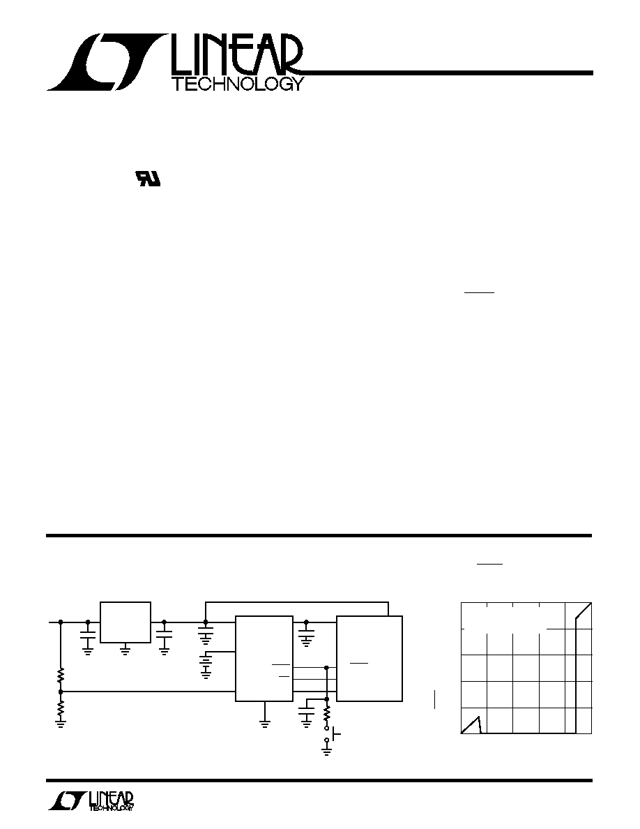
RESET Output Voltage vs
Supply Voltage
+
+
ADJ
V
IN
V
OUT
10
µ
F
V
IN
7.5V
5V
100
µ
F
0.1
µ
F
µ
P NMI
µ
P
POWER
POWER TO
CMOS RAM
I/O LINE
µ
P RESET
µ
P
SYSTEM
0.1µF
3V
51k
10k
LTC692/3 ∑ TA01
LT1086-5
MICROPROCESSOR RESET, BATTERY BACKUP, POWER FAILURE
WARNING AND WATCHDOG TIMING ARE ALL IN A SINGLE CHIP
FOR MICROPROCESSOR SYSTEMS.
LTC692
LTC693
V
BATT
PFI
WDI
RESET
PFO
V
OUT
V
CC
GND
0.1
µ
F
100
Microprocessor
Supervisory Circuits
SUPPLY VOLTAGE (V)
0
RESET OUTPUT VOLTAGE (V)
3
4
5
4
2
1
0
1
2
3
5
T
A
= 25∞C
EXTERNAL PULL-UP = 10µA
V
BATT
= 0V
LTC692/3 ∑ TA02
Æ
U
S
A
O
PPLICATI
s
Critical
µ
P Power Monitoring
s
Intelligent Instruments
s
Battery-Powered Computers and Controllers
s
Automotive Systems
2
LTC692/LTC693
RESET
CONDITIONAL
THRESHOLD
WATCHDOG
BATTERY
POWER FAIL
RAM WRITE
PUSHBUTTON
BATTERY
PINS
(V)
TIMER
BACKUP
WARNING
PROTECT
RESET
BACKUP
LTC692
8
4.40
X
X
X
LTC693
16
4.40
X
X
X
X
LTC690
8
4.65
X
X
X
LTC691
16
4.65
X
X
X
X
LTC694
8
4.65
X
X
X
LTC695
16
4.65
X
X
X
X
LTC699
8
4.65
X
LTC1232
8
4.37/4.62
X
X
LTC1235
16
4.65
X
X
X
X
X
X
LTC694-3.3
8
2.90
X
X
X
LTC695-3.3
16
2.90
X
X
X
X
A
U
G
W
A
W
U
W
A
R
BSOLUTE
XI
TI
S
(Notes 1 and 2)
Terminal Voltage
V
CC
.................................................... ≠ 0.3V to 6.0V
V
BATT
................................................. ≠ 0.3V to 6.0V
All Other Inputs .................. ≠ 0.3V to (V
OUT
+ 0.3V)
Input Current
V
CC
.............................................................. 200mA
V
BATT
............................................................. 50mA
GND............................................................... 20mA
V
OUT
Output Current .................. Short Circuit Protected
Power Dissipation ............................................. 500mW
Operating Temperature Range
LTC692C/LTC693C ............................... 0
∞
C to 70
∞
C
LTC692I/LTC693I ............................ ≠ 40
∞
C to 85
∞
C
Storage Temperature Range ................ ≠ 65
∞
C to 150
∞
C
Lead Temperature (Soldering, 10 sec)................. 300
∞
C
W
U
U
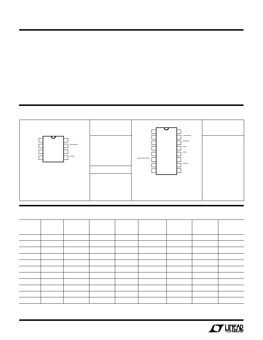
PACKAGE/ORDER I FOR ATIO
ORDER PART
NUMBER
ORDER PART
NUMBER
PRODUCT SELECTIO GUIDE
U
LTC692CN8
LTC692IN8
LTC692CS8
LTC692IS8
S8 PART MARKING
692
692I
T
JMAX
= 110
∞
C,
JA
= 130
∞
C/W (N)
T
JMAX
= 110
∞
C,
JA
= 180
∞
C/W (S)
S8 Package Conditions: PCB Mount on FR4 Material,
Still Air at 25
∞
C, Copper Trace
1
2
3
4
8
7
6
5
TOP VIEW
V
OUT
V
CC
GND
PFI
V
BATT
RESET
WDI
PFO
N8 PACKAGE
8-LEAD PLASTIC DIP
S8 PACKAGE
8-LEAD PLASTIC SOIC
LTC693CN
LTC693IN
LTC693CS
LTC693IS
1
2
3
4
5
6
7
8
TOP VIEW
N PACKAGE
16-LEAD PLASTIC DIP
16
15
14
13
12
11
10
9
V
BATT
V
OUT
V
CC
GND
BATT ON
LOW LINE
OSC IN
OSC SEL
RESET
RESET
WDO
CE IN
CE OUT
WDI
PFO
PFI
S PACKAGE
16-LEAD PLASTIC SOL
T
JMAX
= 110
∞
C,
JA
= 130
∞
C/W (N, S)
S16 Package Conditions: PCB Mount on FR4 Material,
Still Air at 25
∞
C, Copper Trace
(Note 3)
3
LTC692/LTC693
ELECTRICAL C
C
HARA TERISTICS
V
CC
= Full Operating Range, V
BATT
= 2.8V, T
A
= 25
∞
C, unless otherwise noted.
PARAMETER
CONDITONS
MIN
TYP
MAX
UNITS
Battery Backup Switching
Operating Voltage Range
V
CC
4.50
5.50
V
V
BATT
2.00
4.00
V
V
OUT
Output Voltage
I
OUT
= 1mA
V
CC
≠ 0.05
V
CC
≠ 0.005
V
q
V
CC
≠ 0.10
V
CC
≠ 0.005
V
I
OUT
= 50mA
V
CC
≠ 0.50
V
CC
≠ 0.250
V
V
OUT
in Battery Backup Mode
I
OUT
= 250
µ
A, V
CC
< V
BATT
V
BATT
≠ 0.1
V
BATT
≠ 0.02
V
Supply Current (Exclude I
OUT
)
I
OUT
50mA
0.6
1.5
mA
q
0.6
2.5
mA
Supply Current in Battery Backup Mode
V
CC
= 0V, V
BATT
= 2.8V
0.04
1
µ
A
q
0.04
5
µ
A
Battery Standby Current
5.5 > V
CC
> V
BATT
+ 0.2V
≠ 0.1
0.02
µ
A
(+ = Discharge, ≠ = Charge)
q
≠ 1.0
0.10
µ
A
Battery Switchover Threshold
Power Up
70
mV
V
CC
≠ V
BATT
Power Down
50
mV
Battery Switchover Hysteresis
20
mV
BATT ON Output Voltage (Note 4)
I
SINK
= 3.2mA
0.4
V
BATT ON Output Short-Circuit Current (Note 4)
BATT ON = V
OUT
Sink Current
35
mA
BATT ON = 0V Source Current
0.5
1
25
µ
A
Reset and Watchdog Timer
Reset Voltage Threshold
q
4.25
4.40
4.50
V
Reset Threshold Hysteresis
40
mV
Reset Active Time
OSC SEL HIGH, V
CC
= 5V
160
200
240
ms
(Note 5)
q
140
200
280
ms
Watchdog Time-Out Period,
Long Period, V
CC
= 5V
1.2
1.6
2.00
sec
Internal Oscillator
q
1.0
1.6
2.25
sec
Short Period, V
CC
= 5V
80
100
120
ms
q
70
100
140
ms
Watchdog Time-Out Period, External Clock
Long Period
4032
4097
Clock
(Note 6)
Short Period
960
1025
Cycles
Reset Active Time PSRR
1
ms/V
Watchdog Time-Out Period PSRR, Internal OSC
1
ms/V
Minimum WDI Input Pulse Width
V
IL
= 0.4V, V
IH
= 3.5V
q
200
ns
RESET Output Voltage At V
CC
= 1V
I
SINK
= 10
µ
A, V
CC
= 1V
4
200
mV
RESET and LOW LINE Output Voltage
I
SINK
= 1.6mA, V
CC
= 4.25V
0.4
V
(Note 4)
I
SOURCE
= 1
µ
A, V
CC
= 5V
3.5
V
RESET and WDO Output Voltage
I
SINK
= 1.6mA, V
CC
= 5V
0.4
V
(Note 4)
I
SOURCE
= 1
µ
A, V
CC
= 4.25V
3.5
V
4
LTC692/LTC693
The
q
denotes specifications which apply over the full operating
temperature range.
Note 1: Absolute maximum ratings are those values beyond which the life
of the device may be impaired.
Note 2: All voltage values are with respect to GND.
Note 3: For military temperature range, consult the factory.
Note 4: The output pins of BATT ON, LOW LINE, PFO, WDO, RESET and
RESET have weak internal pull-ups of typically 3
µ
A. However, external
pull-up resistors may be used when higher speed is required.
V
CC
= Full Operating Range, V
BATT
= 2.8V, T
A
= 25
∞
C, unless otherwise noted.
ELECTRICAL C
C
HARA TERISTICS
Note 5: The LTC692/LTC693 have minimum reset active times of 140ms
(200ms typically). The reset active time of the LTC693 can be adjusted
(see Table 2 in Applications Information Section).
Note 6: The external clock feeding into the circuit passes through the
oscillator before clocking the watchdog timer (See BLOCK DIAGRAM).
Variation in the time-out period is caused by phase errors which occur
when the oscillator divides the external clock by 64. The resulting variation
in the time-out period is 64 clocks plus one clock of jitter.
Note 7: The input pins of CE IN, OSC IN and OSC SEL have weak internal
pull-ups which pull to the supply when the input pins are floating.
PARAMETER
CONDITONS
MIN
TYP
MAX
UNITS
RESET, RESET, WDO, LOW LINE
Output Source Current
1
3
25
µ
A
Output Short-Circuit Current (Note 4)
Output Sink Current
25
mA
WDI Input Threshold
Logic Low
0.8
V
Logic High
3.5
V
WDI Input Current
WDI = V
OUT
q
4
50
µ
A
WDI = 0V
q
≠ 50
≠ 8
µ
A
Power Fail Detector
PFI Input Threshold
V
CC
= 5V
q
1.25
1.3
1.35
V
PFI Input Threshold PSRR
0.3
mV/V
PFI Input Current
±
0.01
±
25
nA
PFO Output Voltage (Note 4)
I
SINK
= 3.2mA
0.4
V
I
SOURCE
= 1
µ
A
3.5
V
PFO Short Circuit Source Current
PFI = HIGH, PFO = 0V
1
3
25
µ
A
(Note 4)
PFI = LOW, PFO = V
OUT
25
mA
PFI Comparator Response Time (falling)
V
IN
= ≠20mV, V
OD
= 15mV
2
µ
s
PFI Comparator Response Time (rising)
V
IN
= 20mV, V
OD
= 15mV
40
µ
s
(Note 4)
with 10k
Pull-Up
8
µ
s
Chip Enable Gating
CE IN Threshold
V
IL
0.8
V
V
IH
2.0
V
CE IN Pullup Current (Note 7)
3
µ
A
CE OUT Output Voltage
I
SINK
= 3.2mA
0.4
V
I
SOURCE
= 3.0mA
V
OUT
≠ 1.50
V
I
SOURCE
= 1
µ
A, V
CC
= 0V
V
OUT
≠ 0.05
V
CE Propagation Delay
V
CC
= 5V, C
L
= 20pF
20
35
ns
q
20
45
ns
CE OUT Output Short Circuit Current
Output Source Current
30
mA
Output Sink Current
35
mA
Oscillator
OSC IN Input Current (Note 7)
±
2
µ
A
OSC SEL Input Pull-Up Current (Note 7)
5
µ
A
OSC IN Frequency Range
OSC SEL = 0V
q
0
250
kHz
OSC IN Frequency with External Capacitor
OSC SEL = 0V, C
OSC
= 47pF
4
kHz
5
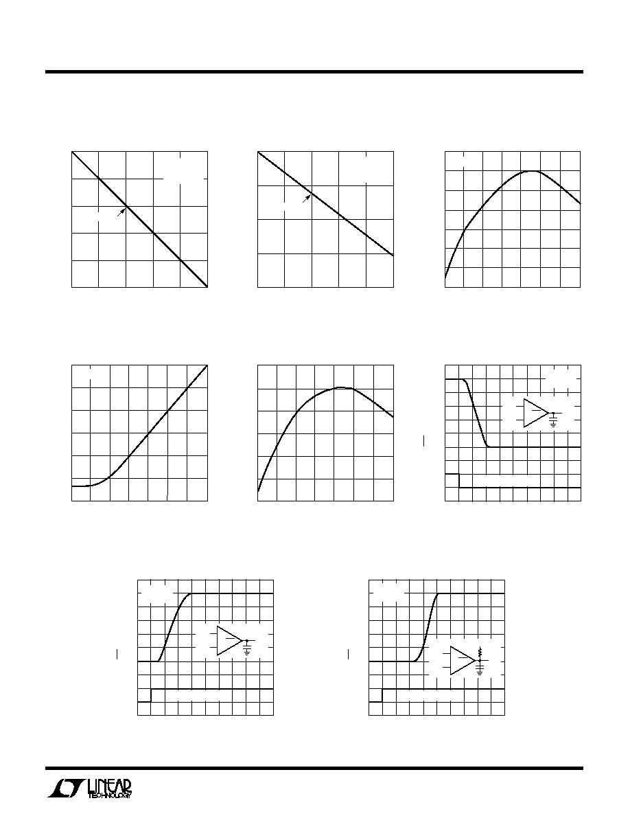
LTC692/LTC693
C
C
HARA TERISTICS
U
W
A
TYPICAL PERFOR
CE
V
OUT
vs I
OUT
V
OUT
vs I
OUT
Power Failure Input Threshold
vs Temperature
LOAD CURRENT (mA)
0
OUTPUT VOLTAGE (V)
4.90
4.95
5.00
40
LTC692/3 ∑ TPC01
4.85
4.80
4.75
10
20
30
50
SLOPE = 5
V
CC
= 5V
V
BATT
= 2.8V
T
A
= 25∞C
LOAD CURRENT (µA)
0
OUTPUT VOLTAGE (V)
2.76
2.78
400
LTC692/3 ∑ TPC02
2.74
2.72
100
200
300
500
2.80
V
CC
= 0V
V
BATT
= 2.8V
T
A
= 25∞C
SLOPE = 125
TEMPERATURE (∞C)
≠50
PFI INPUT THRESHOLD (V)
1.304
1.306
1.308
25
75
LTC692/3 ∑ TPC03
1.302
1.300
≠25
0
50
100
125
1.298
1.296
1.294
V
CC
= 5V
Reset Active Time vs
Temperature
Reset Voltage Threshold
vs Temperature
Power Fail Comparator
Response Time
TEMPERATURE (∞C)
≠50
RESET ACTIVE TIME
216
224
232
25
75
LTC692/3 ∑ TPC04
208
200
≠25
0
50
100
125
192
184
V
CC
= 5V
TEMPERATURE (∞C)
≠50
RESET VOLTAGE THRESHOLD (V)
4.39
4.40
4.41
25
75
LTC692/3 ∑ TPC05
4.38
4.37
≠25
0
50
100
125
4.36
4.35
TIME (µs)
0
4
5
6
4
LTC692/3 ∑ TPC06
3
2
0
1
2
3
5
1
1.305V
1.285V
8
7
6
V
CC
= 5V
T
A
= 25∞C
+
≠
V
PFI
1.3V
PFO
30pF
V
PFI
= 20mV STEP
PFO OUTPUT VOLTAGE (V)
TIME (µs)
0
4
5
6
40
LTC692/3 ∑ TPC07
3
2
0
20
60
1
1.315V
1.295V
120
100
80
V
PFI
= 20mV STEP
180
160
140
V
CC
= 5V
T
A
= 25∞C
+
≠
V
PFI
1.3V
PFO
30pF
PFO OUTPUT VOLTAGE (V)
TIME (µs)
0
4
5
6
4
LTC692/3 ∑ TPC08
3
2
0
2
6
1
1.315V
1.295V
12
10
8
V
PFI
= 20mV STEP
18
16
14
V
CC
= 5V
T
A
= 25∞C
+
≠
V
PFI
1.3V
PFO
30pF
10k
5V
PFO OUTPUT VOLTAGE (V)
Power Fail Comparator
Response Time
Power Fail Comparator Response
Time with Pull-Up Resistor

6
LTC692/LTC693
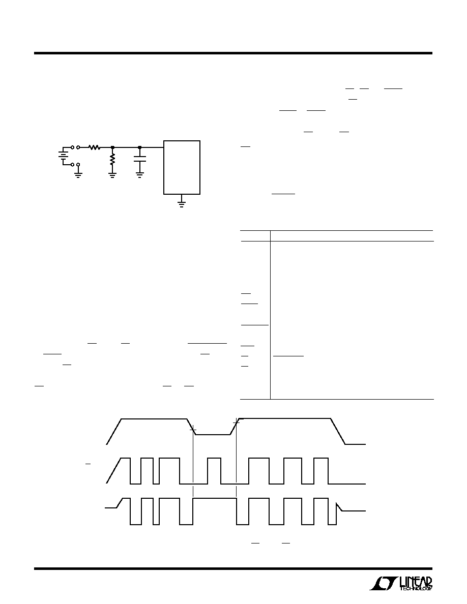
time-out period (see Figure 11). The reset active time is
adjustable on the LTC693. An external pushbutton reset
can be used in connection with the RESET output. See
Pushbutton Reset in the Applications Information section.
RESET: RESET is an Active High Logic Ouput. It is the
inverse of RESET.
LOW LINE: Logic Output from Comparator C1. LOW LINE
indicates a low line condition at the V
CC
input. When V
CC
falls below the reset voltage threshold (4.40V typically),
LOW LINE goes low. As soon as V
CC
rises above the reset
voltage threshold, LOW LINE returns high (see Figure 1).
LOW LINE goes low when V
CC
drops below V
BATT
(see
Table 1).
WDI: Watchdog Input. WDI is a three level input. Driving
WDI either high or low for longer than the watchdog time-
out period, forces both RESET and WDO low. Floating WDI
disables the Watchdog Timer. The timer resets itself with
each transition of the Watchdog Input (see Figure 11).
WDO: Watchdog Logic Output. When the watchdog input
remains either high or low for longer than the watchdog
time-out period, WDO goes low. WDO is set high whenever
there is a transition on the WDI pin, or LOW LINE goes low.
The watchdog timer can be disabled by floating WDI (see
Figure 11).
CE IN: Logic Input to the Chip Enable Gating Circuit. CE IN
can be derived from microprocessor's address line and/or
decoder output. See Applications Information Section and
Figure 5 for additional information.
CE OUT: Logic Output on the Chip Enable Gating Circuit.
When V
CC
is above the reset voltage threshold, CE OUT is a
buffered replica of CE IN. When V
CC
is below the reset
voltage threshold CE OUT is forced high (see Figure 5).
OSC SEL: Oscillator Selection Input. When OSC SEL is
high or floating, the internal oscillator sets the reset active
time and watchdog time-out period. Forcing OSC SEL low
allows OSC IN to be driven from an external clock signal or
an external capacitor to be connected between OSC IN and
GND.
V
CC
: 5V Supply Input. The V
CC
pin should be bypassed
with a 0.1
µ
F capacitor.
V
OUT
: Voltage Output for Backed Up Memory. Bypass with
a capacitor of 0.1
µ
F or greater. During normal operation,
V
OUT
obtains power from V
CC
through an NMOS power
switch, M1, which can deliver up to 50mA and has a typical
ON resistance of 5
. When V
CC
is lower than V
BATT
, V
OUT
is internally switched to V
BATT
. If V
OUT
and V
BATT
are not
used, connect V
OUT
to V
CC
.
V
BATT
: Backup Battery Input. When V
CC
falls below V
BATT
,
auxiliary power connected to V
BATT
, is delivered to V
OUT
through PMOS switch, M2. If backup battery or auxiliary
power is not used, V
BATT
should be connected to GND.
GND: Ground Pin.
BATT ON: Battery On Logic Output from Comparator C2.
BATT ON goes low when V
OUT
is internally connected to
V
CC
. The output typically sinks 35mA and can provide base
drive for an external PNP transistor to increase the output
current above the 50mA rating of V
OUT
. BATT ON goes
high when V
OUT
is internally switched to V
BATT
.
PFI: Power Failure Input. PFI is the noninverting input to
the Power Fail Comparator, C3. The inverting input is
internally connected to a 1.3V reference. The Power Failure
Output remains high when PFI is above 1.3V and goes low
when PFI is below 1.3V. Connect PFI to GND or V
OUT
when
C3 is not used.
PFO: Power Failure Output from C3. PFO remains high
when PFI is above 1.3V and goes low when PFI is below
1.3V. When V
CC
is lower than V
BATT
, C3 is shut down and
PFO is forced low.
RESET: Logic Output for
µ
P Reset Control. Whenever V
CC
falls below either the reset voltage threshold (4.40V
typically) or V
BATT
, RESET goes active low. After V
CC
returns to 5V, reset pulse generator forces RESET to
remain active low for a minimum of 140ms. When the
watchdog timer is enabled but not serviced prior to a preset
time-out period, reset pulse generator also forces RESET
to active low for a minimum of 140ms for every preset
PI FU CTIO S
U
U
U
7
LTC692/LTC693
PI FU CTIO S
U
U
U
OSC IN: Oscillator Input. OSC IN can be driven by an
external clock signal or an external capacitor can be
connected between OSC IN and GND when OSC SEL is
forced low. In this configuration the nominal reset active
time and watchdog time-out period are determined by
the number of clocks or set by the formula (see
Applications Information section). When OSC SEL is
high or floating, the internal oscillator is enabled and the
reset active time is fixed at 200ms typical. OSC IN selects
between the 1.6 seconds and 100ms typical watchdog
time-out periods. In both cases the time-out period
immediately after a reset is 1.6 seconds typical.
W
I
D AGRA
BLOCK
CHARGE
PUMP
M2
M1
VBATT
VCC
CE IN
PFI
OSC IN
OSC SEL
WDI
RESET PULSE
GENERATOR
WATCHDOG
TIMER
RESET
BATT ON
VOUT
C1
1.3V
GND
≠
+
≠
+
C2
OSC
TRANSITION
DETECTOR
≠
+
C3
WDO
RESET
PFO
LOW LINE
CE OUT
LTC692/3 ∑ BD
8
LTC692/LTC693
Microprocessor Reset
The LTC692/LTC693 use a bandgap voltage reference and
a precision voltage comparator C1 to monitor the 5V
supply input on V
CC
(see BLOCK DIAGRAM). When V
CC
falls below the reset voltage threshold, the RESET output
is forced to active low state. The reset voltage threshold
accounts for a 10% variation on V
CC
, so the RESET output
becomes active low when V
CC
falls below 4.50V (4.40V
typical). On power-up, the RESET signal is held active low
for a minimum of 140ms after reset voltage threshold is
reached to allow the power supply and microprocessor to
stabilize. The reset active time is adjustable on the LTC693.
On power-down, the RESET signal remains active low
even with V
CC
as low as 1V. This capability helps hold the
microprocessor in stable shutdown condition. Figure 1
shows the timing diagram of the RESET signal.
The precision voltage comparator, C1, typically has 40mV
of hysteresis which ensures that glitches at the V
CC
pin do
not activate the RESET output. Response time is typically
10
µ
s. To help prevent mistriggering due to transient loads,
V
CC
pin should be bypassed with a 0.1
µ
F capacitor with the
leads trimmed as short as possible.
The LTC693 has two additional outputs: RESET and LOW
LINE. RESET is an active high output and is the inverse of
RESET. LOW LINE is the output of the precision voltage
comparator C1. When V
CC
falls below the reset voltage
threshold, LOW LINE goes low. LOW LINE returns high as
soon as V
CC
rises above the reset voltage threshold.
Battery Switchover
The battery switchover circuit compares V
CC
to the
V
BATT
input, and connects V
OUT
to whichever is higher.
When V
CC
rises to 70mV above V
BATT
, the battery
switchover comparator, C2, connects V
OUT
to V
CC
through
a charge pumped NMOS power switch, M1. When V
CC
falls to 50mV above V
BATT
, C2 connects V
OUT
to V
BATT
through a PMOS switch, M2. C2 has typically 20mV of
hysteresis to prevent spurious switching when V
CC
remains nearly equal to V
BATT
. The response time of C2
is approximately 20
µ
s.
During normal operation, the LTC692/LTC693 use a charge
pumped NMOS power switch to achieve low dropout and
low supply current. This power switch can deliver up to
50mA to V
OUT
from V
CC
and has a typical "on" resistance
of 5
. The V
OUT
pin should be bypassed with a capacitor
of 0.1
µ
F or greater to ensure stability. Use of a larger
bypass capacitor is advantageous for supplying current to
heavy transient loads.
When operating currents larger than 50mA are required
from V
OUT
, or a lower dropout (V
CC
≠ V
OUT
voltage differ-
ential) is desired, the LTC693 should be used. This prod-
uct provides BATT ON output to drive the base of the
external PNP transistor (Figure 2). If higher currents are
needed with the LTC692, a high current Schottky diode
can be connected from the V
CC
pin to the V
OUT
pin to
supply the extra current.
U
S
A
O
PPLICATI
W
U
U
I FOR ATIO
V
CC
t1
t1 = RESET ACTIVE TIME
V1 = RESET VOLTAGE THRESHOLD
V2 = RESET VOLTAGE THRESHOLD +
RESET THRESHOLD HYSTERESIS
t1
V2
V2
V1
V1
LTC692/3 ∑ F01
RESET
LOW LINE
Figure 1. Reset Active Time
9
LTC692/LTC693
memory backup instead of a battery. The charging resistor
for the rechargeable batteries should be connected to
V
OUT
since this eliminates the discharge path that exists
when the resistor is connected to V
CC
(Figure 3).
Replacing the Backup Battery
When changing the backup battery with system power
on, spurious resets can occur while the battery is re-
moved due to battery standby current. Although battery
standby current is only a tiny leakage current, it can still
charge up the stray capacitance on the V
BATT
pin. The
oscillation cycle is as follows: When V
BATT
reaches within
50mV of V
CC
, the LTC692/LTC693 switch to battery
backup. V
OUT
pulls V
BATT
low and the devices go back to
normal operation. The leakage current then charges up
the V
BATT
pin again and the cycle repeats.
If spurious resets during battery replacement pose no
problems, then no action is required. Otherwise, a resistor
from V
BATT
to GND will hold the pin low while changing the
battery. For example, the battery standby current is 1
µ
A
maximum over temperature and the external resistor
required to hold V
BATT
below V
CC
is:
With V
CC
= 4.25V, a 3.9M resistor will work. With a 3V
battery, this resistor will draw only 0.77
µ
A from the
battery, which is negligible in most cases.
U
S
A
O
PPLICATI
W
U
U
I FOR ATIO
The LTC692/LTC693 are protected for safe area operation
with a short circuit limit. Output current is limited to
approximately 200mA. If the device is overloaded for long
periods of time, thermal shutdown turns the power switch
off until the device cools down. The threshhold tempera-
ture for thermal shutdown is approximately 155
∞
C with
about 10
∞
C of hysteresis which prevents the device from
oscillating in and out of shutdown.
The PNP switch used in competitive devices was not
chosen for the internal power switch because it injects
unwanted current into the substrate. This current is col-
lected by the V
BATT
pin in competitive devices and adds to
the charging current of the battery which can damage
lithium batteries. The LTC692/LTC693 use a charge pumped
NMOS power switch to eliminate unwanted charging
current while achieving low dropout and low supply cur-
rent. Since no current goes to the substrate, the current
collected by the V
BATT
pin is strictly junction leakage.
A 125
PMOS switch connects the V
BATT
input to V
OUT
in
battery backup mode. The switch is designed for very low
dropout voltage (input-to-output differential). This feature
is advantageous for low current applications such as
battery backup in CMOS RAM and other low power CMOS
circuitry. The supply current in battery backup mode is
1
µ
A maximum.
The operating voltage at the V
BATT
pin ranges from 2.0V to
4.0V. High value capacitors, such as electrolytic or farad-
size double layer capacitors, can be used for short term
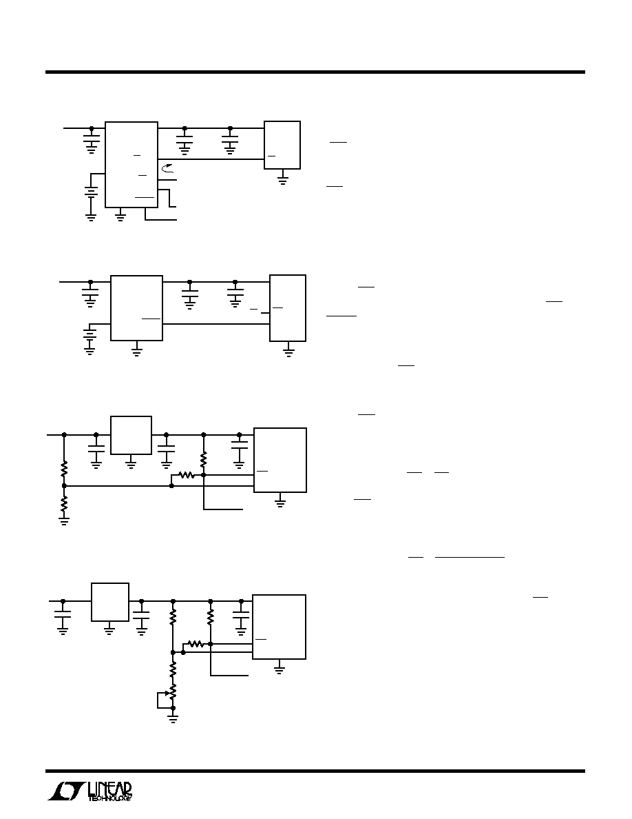
Figure 2. Using BATT ON to Drive External PNP Transistor
5V
3V
0.1µF
0.1µF
V
BATT
V
CC
LTC693
V
OUT
GND
4
3
1
2
5
ANY PNP POWER TRANSISTOR
LTC692/3 ∑ F02
BATT ON
Figure 3. Charging External Battery Through V
OUT
5V
3V
0.1µF
0.1µF
LTC692/3 ∑ F03
V
OUT
≠ V
BATT
R
I =
R
V
BATT
V
CC
LTC692
LTC693
V
OUT
GND
R
V
≠ 50mV
1 A
CC
µ
10
LTC692/LTC693
V
CC
V1
CE IN
V
OUT
= V
BATT
CE OUT
V
OUT
= V
BATT
V2
V1 = RESET VOLTAGE THRESHOLD
V2 = RESET VOLTAGE THRESHOLD +
RESET THRESHOLD HYSTERESIS
LTC692/3 ∑ F05
Memory Protection
The LTC693 includes memory protection circuitry which
ensures the integrity of the data in memory by preventing
write operations when V
CC
is at an invalid level. Two
additional pins, CE IN and CE OUT, control the Chip Enable
or Write inputs of CMOS RAM. When V
CC
is 5V, CE OUT
follows CE IN with a typical propagation delay of 20ns.
When V
CC
falls below the reset voltage threshold or V
BATT
,
CE OUT is forced high, independent of CE IN. CE OUT is an
U
S
A
O
PPLICATI
W
U
U
I FOR ATIO
If battery connections are made through long wires, a 10
to 100
series resistor and a 0.1
µ
F capacitor are recom-
mended to prevent any overshoot beyond V
CC
due to the
lead inductance (Figure 4).
alternative signal to drive the CE, CS, or Write input of
battery backed up CMOS RAM. CE OUT can also be used
to drive the Store or Write input of an EEPROM, EAROM or
NOVRAM to achieve similar protection. Figure 5 shows the
timing diagram of CE IN and CE OUT.
CE IN can be derived from the microprocessor's address
decoder output. Figure 6 shows a typical nonvolatile
CMOS RAM application.
Memory protection can also be achieved with the LTC692
by using RESET as shown in Figure 7.
SIGNAL
STATUS
V
CC
C2 monitors V
CC
for active switchover.
V
OUT
V
OUT
is connected to V
BATT
through an internal PMOS switch.
V
BATT
The supply current is 1
µ
A maximum.
BATT ON
Logic high. The open-circuit output voltage is equal to V
OUT
.
PFI
Power Failure Input is ignored.
PFO
Logic low
RESET
Logic low
RESET
Logic high. The open-circuit output voltage is equal to V
OUT
.
LOW LINE Logic low
WDI
Watchdog Input is ignored.
WDO
Logic high. The open-circuit output voltage is equal to V
OUT
.
CE IN
Chip Enable Input is ignored.
CE OUT
Logic high. The open-circuit output voltage is equal to V
OUT
.
OSC IN
OSC IN is ignored.
OSC SEL
OSC SEL is ignored.
Table 1. Input and Output Status in Battery Backup Mode
3.9M
0.1µF
V
BATT
LTC692
LTC693
GND
LTC692/3 ∑ F04
10
Figure 4. 10
/0.1
µ
F combination eliminates inductive
overshoot and prevents spurious resets during battery
replacement.
Table 1 shows the state of each pin during battery backup.
When the battery switchover section is not used, connect
V
BATT
to GND and V
OUT
to V
CC
.
Figure 5. Timing Diagram for CE IN and CE OUT
11
LTC692/LTC693
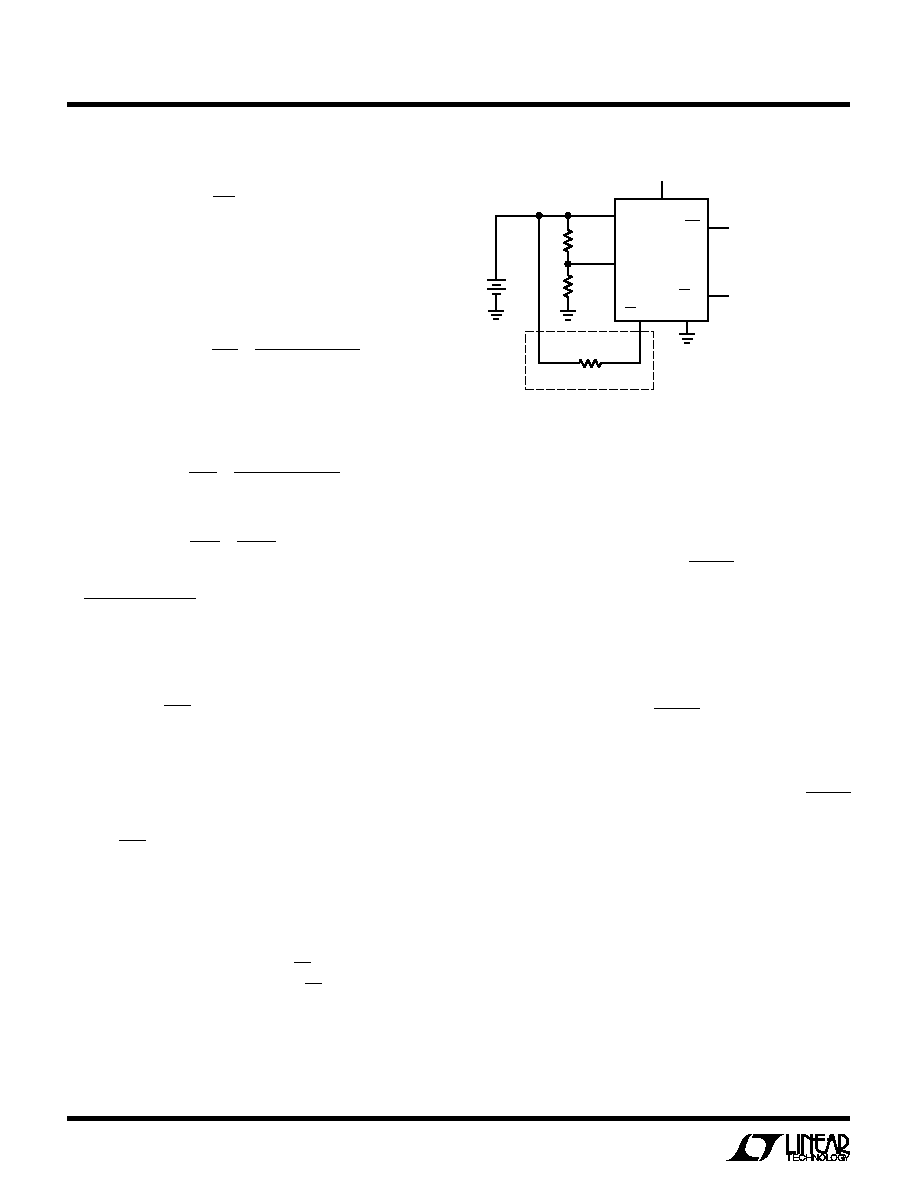
Power Fail Warning
The LTC692/LTC693 generate a Power Failure Output
(PFO) for early warning of failure in the microprocessor's
power supply. This is accomplished by comparing the
Power Failure Input (PFI) with an internal 1.3V reference.
PFO goes low when the voltage at the PFI pin is less than
1.3V. Typically PFI is driven by an external voltage divider
(R1 and R2 in Figures 8 and 9) which senses either an
unregulated DC input or a regulated 5V output. The voltage
divider ratio can be chosen such that the voltage at the PFI
pin falls below 1.3V, several milliseconds before the 5V
supply falls below the maximum reset voltage threshold of
4.50V. PFO is normally used to interrupt the microproces-
sor to execute shutdown procedure between PFO and
RESET or RESET.
The power fail comparator, C3, does not have hysteresis.
Hysteresis can be added however, by connecting a resis-
tor between the PFO output and the noninverting PFI input
pin as shown in Figures 8 and 9. The upper and lower trip
points in the comparator are established as follows:
When PFO output is low, R3 sinks current from the
summing junction at the PFI pin.
When PFO output is high, the series combination of R3 and
R4 source current into the PFI summing junction.
Example 1: The circuit in Figure 8 demonstrates the use of
the power fail comparator to monitor the unregulated
power supply input. Assuming the the rate of decay of the
supply input V
IN
is 100mV/ms and the total time to execute
a shutdown procedure is 8ms. Also, the noise of V
IN
is
200mV. With these assumptions in mind, we can reason-
ably set V
L
= 7.25V which is 1.25V greater than the sum of
maximum reset voltage threshold and the dropout voltage
of LT1086-5 (4.5V + 1.5V) and V
HYSTERESIS
= 850mV.
U
S
A
O
PPLICATI
W
U
U
I FOR ATIO
Figure 6. A Typical Nonvolatile CMOS RAM Application
5V
3V
0.1
µ
F
10
µ
F
V
BATT
V
CC
LTC693
V
OUT
GND
LTC692/3 ∑ F06
V
CC
RESET
CE IN
CE OUT
RESET
0.1
µ
F
TO
µ
P
FROM DECODER
CS
20ns PROPAGATION DELAY
62512
RAM
+
GND
Figure 7. Write Protect for RAM with the LTC692
5V
3V
0.1
µ
F
10
µ
F
V
BATT
V
CC
LTC692
V
OUT
GND
LTC692/3 ∑ F07
V
CC
RESET
0.1
µ
F
CS
62128
RAM
CS1
CS2
GND
+
V = 1.3V 1+
R1
R2
R1
R3
H
+
V
1.3V 1
R1
R2
≠
(5V ≠ 1.3V)R1
1.3V(R3 R4)
L
=
+
+
Assuming R4
R3,V
5V
R1
R3
HYSTERESIS
<<
=
10
µ
F
10
µ
F
V
IN
V
OUT
ADJ
LTC692/3 ∑ F09
0.1
µ
F
TO
µ
P
LT1086-5
V
IN
6.5V
R4
10k
+
R1
27k
R3
2.7M
R2
8.2k
+
5V
R5
3.3k
V
CC
GND
PFO
PFI
LTC692
LTC693
Figure 9. Monitoring
Regulated DC Supply
with the LTC692/LTC693 Power Fail Comparator
10
µ
F
100
µ
F
V
IN
V
OUT
ADJ
LTC692/3 ∑ F08
V
CC
0.1
µ
F
TO
µ
P
PFO
GND
LT1086-5
V
IN
7.5V
R4
10k
PFI
LTC692
LTC693
R1
51k
R2
10k
R3
300k
+
+
5V
Figure 8. Monitoring
Unregulated DC Supply with the
LTC692/LTC693 Power Fail Comparator
12
LTC692/LTC693
U
S
A
O
PPLICATI
W
U
U
I FOR ATIO
Figure 10. Backup Battery Monitor with Optional Test Load
Watchdog Timer
The LTC692/LTC693 provide a watchdog timer function to
monitor the activity of the microprocessor. If the micro-
processor does not toggle the Watchdog Input (WDI)
within a seleced time-out period, RESET is forced to active
low for a minimum of 140ms. The reset active time is
adjustable on the LTC693. Since many systems cannot
service the watchdog timer immediately after a reset, the
LTC693 has longer time-out period (1.0 second mini-
mum) right after a reset is issued. The normal time-out
period (70ms minimum) becomes effective following the
first transition of WDI after RESET is inactive. The watch-
dog time-out period is fixed at a 1.0 second minimum on
the LTC692. Figure 11 shows the timing diagram of
watchdog time-out period and reset active time. The
watchdog time-out period is restarted as soon as RESET
is inactive. When either a high-to-low or low-to-high
transition occurs at the WDI pin prior to time-out, the
watchdog timer is reset and begins to time-out again. To
ensure the watchdog timer does not time-out, either a
high-to-low or low-to-high transition on the WDI pin must
occur at or less than the minimum time-out period. If the
input to the WDI pin remains either high or low, reset
pulses will be issued every 1.6 seconds typically. The
watchdog timer can be deactivated by floating the WDI pin.
The timer is also disabled when V
CC
falls below the reset
voltage threshold or V
BATT
.
Choose R3 = 300k and R1 = 51k. Also select R4 = 10k
which is much smaller than R3.
R2 = 10.1k, Choose nearest 5% resistor 10k and recalcu-
late V
L
,
V
HYSTERESIS
= 8.151V ≠ 7.32V = 831mV
The 10.7ms allows enough time to execute shutdown
procedure for microprocessor and 831mV of hysteresis
would prevent PFO from going low due to the noise of V
IN
.
Example 2: The circuit in Figure 9 can be used to measure
the regulated 5V supply to provide early warning of power
failure. Because of variations in the PFI threshold, this
circuit requires adjustment to ensure the PFI comparator
trips before the reset threshold is reached. Adjust R5 such
that the PFO output goes low when the V
CC
supply reaches
the desired level (e.g., 4.6V).
Monitoring the Status of the Battery
C3 can also monitor the status of the memory backup
battery (Figure 10). If desired, the CE OUT can be used to
apply a test load to the battery. Since CE OUT is forced high
in battery backup mode, the test load will not be applied to
the battery while it is in use, even if the microprocessor is
not powered.
R3
5.88 R1
(7.32V ≠ 6.25V)
100mV/ms
10.7ms
=
V
1.3V 1
10k
≠
(5V ≠ 1.3V)51
1.3V(310k
L
=
+
=
51
7 32
k
k
)
.
V
V
1.3V 1
51k
10k
51k
300k
8.151V
H
=
+
+
=
3V
5V
LTC692/3 ∑ F10
R1
1M
R
L
20K
R2
1M
OPTIONAL TEST LOAD
LOW BATTERY SIGNAL
TO
µ
P I/O PIN
I/O PIN
V
CC
V
BATT
GND
PFI
LTC693
CE IN
PFO
CE OUT
7.25V = 1.3V 1+
R2
≠
(5V ≠ 1.3V)51
51
1 3 310
k
k
V
k
.
(
)
V
5V
R1
R3
850mV
HYSTERESIS
=
=
13
LTC692/LTC693
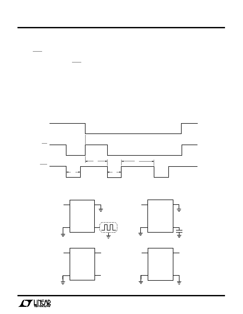
Figure 12. Oscillator Configurations
U
S
A
O
PPLICATI
W
U
U
I FOR ATIO
The LTC693 provides an additional output (Watchdog
Output, WDO) which goes low if the watchdog timer is
allowed to time out and remains low until set high by the
next transition on the WDI pin. WDO is also set high when
V
CC
falls below the reset voltage threshold or V
BATT
.
The LTC693 has two additonal pins OSC SEL and OSC IN,
which allow reset active time and watchdog time-out
period to be adjusted per Table 2. Several configurations
are shown in Figure 12.
OSC IN can be driven by an external clock signal or an
external capacitor can be connected between OSC IN and
GND when OSC SEL is forced low. In these configurations,
the nominal reset active time and watchdog time-out
period are determined by the number of clocks or set by
the formula in Table 2. When OSC SEL is high or floating,
the internal oscillator is enabled and the reset active time
is fixed at 140ms minimum. OSC IN selects between the
1 second and 70ms minimum normal watchdog time-out
periods. In both cases, the time-out period immediately
after a reset is at least 1 second.
Figure 11. Watchdog Time-out Period and Reset Active Time
t1 = RESET ACTIVE TIME
t2 = NORMAL WATCHDOG TIME-OUT PERIOD
t3 = WATCHDOG TIME-OUT PERIOD IMMEDIATELY
AFTER A RESET
V
CC
= 5V
t2
t3
t1
t1
WDO
WDI
RESET
LTC692/3 ∑ F11
EXTERNAL CLOCK
INTERNAL OSCILLATOR
1.6 SECOND WATCHDOG
INTERNAL OSCILLATOR
100ms WATCHDOG
EXTERNAL OSCILLATOR
GND
GND
GND
GND
V
CC
V
CC
V
CC
OSC SEL
OSC SEL
OSC SEL
OSC SEL
OSC IN
OSC IN
OSC IN
OSC IN
3
3
3
3
4
4
4
4
8
8
8
8
7
7
7
7
V
CC
FLOATING
OR HIGH
FLOATING
OR HIGH
LTC693
FLOATING
OR HIGH
LTC693
LTC693
LTC693
LTC692/3 ∑ F12
5V
5V
5V
5V
14
LTC692/LTC693
Low
External Clock Input
1024 clks
4096 clks
2048 clks
Low
External Capacitor*
Floating or High
Low
100ms
1.6 sec
200ms
Floating or High
Floating or High
1.6 sec
1.6 sec
200ms
U
S
A
O
PPLICATI
W
U
U
I FOR ATIO
OSC IN
OSC SEL
*The nominal internal frequency is 10.24kHz. The nominal oscillator frequency with external capacitor is F
OSC
(Hz) =
Pushbutton Reset
The LTC692/LTC693 do not provide a logic input for direct
connection to a pushbutton. However, a pushbutton in
series with a 100
resistor connected to the RESET output
pin (Figure 13) provides an alternative for manual reset.
Connecting a 0.1
µ
F capacitor to the RESET pin debounces
the pushbutton input.
The 100
resistor in series with the pushbutton is re-
quired to prevent the ringing, due to the capacitance and
lead inductance, from pulling the RESET pins of the MPU
and LTC692/LT693 below ground.
Figure 13. The External Pushbutton Reset
184,000
C(pF)
WATCHDOG TIME-OUT PERIOD
RESET ACTIVE TIME
IMMEDIATELY
AFTER RESET
(Long Period)
NORMAL
(Short Period)
LTC693
Table 2. LTC693 Reset Active Time and Watchdog Time-Out Selections
400ms
◊
C
47pF
1.6 sec
◊
C
47pF
800ms
◊
C
47pF
5V
100
V
CC
LTC692
LTC693
GND
LTC692/3 ∑ F13
RESET
0.1
µ
F
MPU
(e.g. 6805)
RESET
U
S
A
O
PPLICATI
TYPICAL
Capacitor Backup with 74HC4016 Switch
R1
10k
R2
30k
0.1
µ
F
0.1
µ
F
+
14
12
11
10
1
7
100
µ
F
13
2
5V
V
CC
V
OUT
V
BATT
74HC4016
LTC692/3 ∑ TA3
LOW LINE
GND
LTC693
15
LTC692/LTC693
U
S
A
O
PPLICATI
TYPICAL
Write Protect for Additional RAMs
N8 Package
8-Lead Plastic DIP
Dimensions in inches (millimeters) unless otherwise noted.
PACKAGE DESCRIPTIO
U
N8 0393
0.045 ± 0.015
(1.143 ± 0.381)
0.100 ± 0.010
(2.540 ± 0.254)
0.065
(1.651)
TYP
0.045 ≠ 0.065
(1.143 ≠ 1.651)
0.130 ± 0.005
(3.302 ± 0.127)
0.020
(0.508)
MIN
0.018 ± 0.003
(0.457 ± 0.076)
0.125
(3.175)
MIN
0.009 ≠ 0.015
(0.229 ≠ 0.381)
0.300 ≠ 0.320
(7.620 ≠ 8.128)
0.325
+0.025
≠0.015
+0.635
≠0.381
8.255
(
)
1
2
3
4
8
7
6
5
0.250 ± 0.010
(6.350 ± 0.254)
0.400
(10.160)
MAX
1
2
3
4
0.150 ≠ 0.157
(3.810 ≠ 3.988)
8
7
6
5
0.189 ≠ 0.197
(4.801 ≠ 5.004)
0.228 ≠ 0.244
(5.791 ≠ 6.197)
0.016 ≠ 0.050
0.406 ≠ 1.270
0.010 ≠ 0.020
(0.254 ≠ 0.508)
◊
45
∞
0∞≠ 8∞ TYP
0.008 ≠ 0.010
(0.203 ≠ 0.254)
SO8 0393
0.053 ≠ 0.069
(1.346 ≠ 1.752)
0.014 ≠ 0.019
(0.355 ≠ 0.483)
0.004 ≠ 0.010
(0.101 ≠ 0.254)
0.050
(1.270)
BSC
S8 Package
8-Lead Plastic SOIC
10
µ
F
V
BATT
V
CC
LTC693
V
OUT
GND
LTC692/3 ∑ TA04
V
CC
LOW LINE
CE IN
CE OUT
0.1
µ
F
CS
20ns PROPAGATION
DELAY
62512
RAM
A
5V
3V
0.1
µ
F
+
V
CC
62128
RAM
C
V
CC
CS
2
62128
RAM
B
CS
A
CS
B
CS
C
CS
1
CS
1
OPTIONAL CONNECTION FOR
ADDITIONAL RAMs
CS
2
0.1
µ
F
0.1
µ
F
Information furnished by Linear Technology Corporation is believed to be accurate and reliable.
However, no responsibility is assumed for its use. Linear Technology Corporation makes no represen-
tation that the interconnection of circuits as described herein will not infringe on existing patent rights.
16
LTC692/LTC693
Linear Technology Corporation
1630 McCarthy Blvd., Milpitas, CA 95035-7487
(408) 432-1900
q
FAX
: (408) 434-0507
q
TELEX
: 499-3977
PACKAGE DESCRIPTIO
U
Dimensions in inches (millimeters) unless otherwise noted.
N Package
16-Lead Plastic DIP
0.260 ± 0.010
(6.604 ± 0.254)
0.770
(19.558)
MAX
16
1
2
3
4
5
6
7
8
9
10
11
12
13
14
15
N16 0393
0.015
(0.381)
MIN
0.125
(3.175)
MIN
0.130 ± 0.005
(3.302 ± 0.127)
0.065
(1.651)
TYP
0.045 ≠ 0.065
(1.143 ≠ 1.651)
0.018 ± 0.003
(0.457 ± 0.076)
0.045 ± 0.015
(1.143 ± 0.381)
0.100 ± 0.010
(2.540 ± 0.254)
0.009 ≠ 0.015
(0.229 ≠ 0.381)
0.300 ≠ 0.325
(7.620 ≠ 8.255)
0.325
+0.025
≠0.015
+0.635
≠0.381
8.255
(
)
S Package
16-Lead SOL
NOTE:
1. PIN 1 IDENT, NOTCH ON TOP AND CAVITIES ON THE BOTTOM OF PACKAGES ARE THE MANUFACTURING OPTIONS.
THE PART MAY BE SUPPLIED WITH OR WITHOUT ANY OF THE OPTIONS.
NOTE 1
0.398 ≠ 0.413
(10.109 ≠ 10.490)
(NOTE 2)
16
15
14
13
12
11
10
9
1
2
3
4
5
6
7
8
S16 0393
0.394 ≠ 0.419
(10.007 ≠ 10.643)
0.037 ≠ 0.045
(0.940 ≠ 1.143)
0.004 ≠ 0.012
(0.102 ≠ 0.305)
0.093 ≠ 0.104
(2.362 ≠ 2.642)
0.050
(1.270)
TYP
0.014 ≠ 0.019
(0.356 ≠ 0.482)
TYP
0∞ ≠ 8∞ TYP
NOTE 1
0.005
(0.127)
RAD MIN
0.009 ≠ 0.013
(0.229 ≠ 0.330)
0.016 ≠ 0.050
(0.406 ≠ 1.270)
0.291 ≠ 0.299
(7.391 ≠ 7.595)
(NOTE 2)
◊
45
∞
0.010 ≠ 0.029
(0.254 ≠ 0.737)
2. THESE DIMENSIONS DO NOT INCLUDE MOLD FLASH OR PROTRUSIONS.
MOLD FLASH OR PROTRUSIONS SHALL NOT EXCEED 0.006 INCH (0.15mm).
©
LINEAR TECHNOLOGY CORPORATION 1993
LT/GP 0493 10K REV 0