 | –≠–ª–µ–∫—Ç—Ä–æ–Ω–Ω—ã–π –∫–æ–º–ø–æ–Ω–µ–Ω—Ç: RH1078M | –°–∫–∞—á–∞—Ç—å:  PDF PDF  ZIP ZIP |

1
RH1078M
Micropower, Dual, Single Supply
Precision Op Amp
The RH1078M is a micropower dual op amp in the
standard 8-pin configuration. This device is optimized for
single supply operation at 5V. Specifications for
±
15V are
also provided.
The wafer lots are processed to LTC's in-house Class S
flow to yield circuits usable in stringent military applica-
tions.
D
U
ESCRIPTIO
A
U
G
W
A
W
U
W
A
R
BSOLUTE
XI
TI
S
Supply Voltage .....................................................
±
22V
Differential Input Voltage ......................................
±
30V
Input Voltage ............... Equal to Positive Supply Voltage
............................... 0.5V Below Negative Supply Voltage
Output Short-Circuit Duration ......................... Indefinite
Operating Temperature Range ............. ≠ 55
∞
C to 125
∞
C
Storage Temperature Range ................ ≠ 55
∞
C to 150
∞
C
Lead Temperature (Soldering, 10 sec) ................. 300
∞
C
W
U
U
PACKAGE/ORDER I FOR ATIO
BUR -I CIRCUIT
U U
≠
+
50k
100
50k
20V
≠20V
(Each Amplifier)
TOTAL DOSE BIAS CIRCUIT
TOP VIEW
OUT B
OUT A
V
+
≠IN B
≠IN A
+IN B
+IN A
V
≠
8
7
6
5
3
2
1
4
H PACKAGE
8-LEAD TO-5 METAL CAN
≠
+
10k
10k
15V
8V
≠15V
Note: For ordering information contact LTC.

2
RH1078M
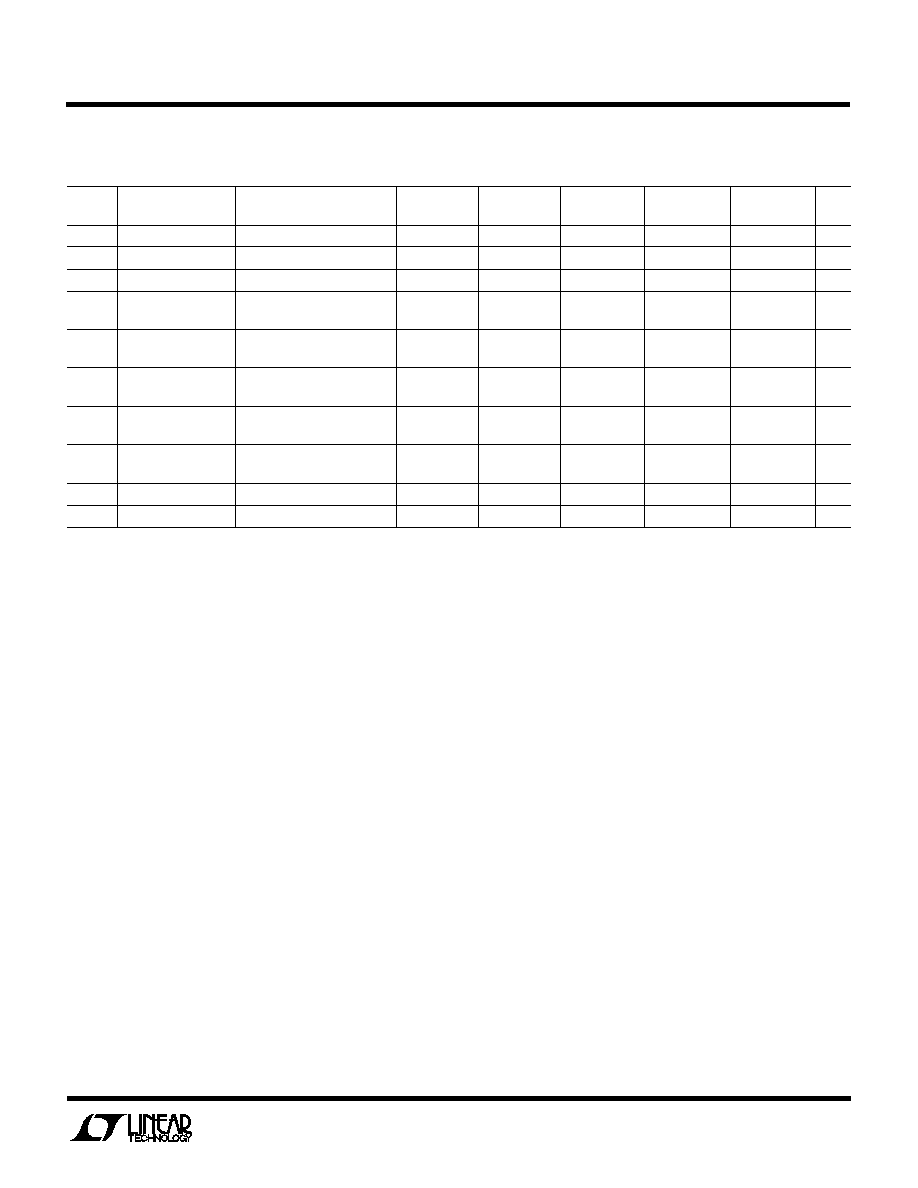
TABLE 1: ELECTRICAL CHARACTERISTICS
V
S
= 5V, V
CM
= 0.1V, V
OUT
= 1.4V unless otherwise specified.
(Preirradiation)
T
A
= 25
∞
C
SUB-
SUB-
SYMBOL
PARAMETER
CONDITIONS
NOTES MIN
TYP MAX GROUP MIN
TYP
MAX GROUP
UNITS
V
OS
Input Offset Voltage
120
4
370
2, 3
µ
V
V
OS
Average Tempco of
0.5
µ
V/
∞
C
Temp
Offset Voltage
V
OS
Long Term V
OS
Stability
0.5
µ
V/Month
Time
I
OS
Input Offset Current
0.8
1
1.5
2, 3
nA
I
B
Input Bias Current
15
1
18
2, 3
nA
e
n
Input Noise Voltage
0.1Hz to 10Hz
1
0.5
µ
VP-P
Input Noise Voltage Density
f
O
= 10Hz
1
25
nV/
Hz
f
O
= 1kHz
1
24
nV/
Hz
i
n
Input Noise Current
0.1Hz to 10Hz
1
2.6
pAP-P
Input Noise Current Density
f
O
= 10Hz
1
0.07
pA/
Hz
f
O
= 1kHz
1
0.025
pA/
Hz
R
IN
Input Resistance Differential
2
600
M
Common Mode
2
5
G
Input Voltage Range
2
3.5
1
3.20
2, 3
V
2
0
1
0.05
2, 3
V
CMRR
Common-Mode
V
CM
= 0V to 3.5V
94
1
dB
Rejection Ratio
V
CM
= 0.05V to 3.2V
88
2, 3
dB
PSRR
Power Supply
V
S
= 2.3V to 12V
100
1
dB
Rejection Ratio
V
S
= 3.1V to 12V
94
2, 3
dB
A
VOL
Large-Signal Voltage Gain
V
O
= 0.03V to 4V, No Load
150
1
V/mV
V
O
= 0.03V to 3.5V, R
L
= 50k
120
1
V/mV
V
O
= 0.05V to 4V, No Load
80
2, 3
V/mV
V
O
= 0.05V to 3.5V, R
L
= 50k
60
2, 3
V/mV
V
OUT
Output Voltage Swing
Output Low, No Load
6
4
8
5, 6
mV
Output Low, 2k to GND
2
4
mV
Output Low, I
SINK
= 100
µ
A
130
4
170
5, 6
mV
Output High, No Load
4.2
4
3.9
5, 6
V
Output High, 2k to GND
3.5
4
3.0
5, 6
V
SR
Slew Rate
A
V
= 1, V
S
=
±
2.5V
0.04
4
V/
µ
s
GBW
Gain-Bandwidth Product
f
O
20kHz
200
kHz
I
S
Supply Current
per Amplifier
75
1
95
2, 3
µ
A
Channel Separation
V
IN
= 3V, R
L
= 10k
130
dB
Minimum Supply Voltage
3
2.3
V
≠ 55
∞
C
T
A
125
∞
C

3
RH1078M
TABLE 1: ELECTRICAL CHARACTERISTICS
V
S
=
±
15V unless otherwise specified.
T
A
= 25
∞
C
SUB-
SUB-
SYMBOL
PARAMETER
CONDITIONS
NOTES
MIN
TYP MAX GROUP MIN
TYP
MAX GROUP
UNITS
V
OS
Input Offset Voltage
350
4
600
2, 3
µ
V
V
OS
Average Tempco of
0.6
µ
V/
∞
C
Temp
Offset Voltage
I
OS
Input Offset Current
0.8
1
1.5
2, 3
nA
I
B
Input Bias Current
15
18
2, 3
nA
Input Voltage Range
13.5
1
V
≠15.0
1
V
CMRR
Common-Mode
V
CM
= 13.5V, ≠ 15V
97
1
dB
Rejection Ratio
V
CM
= 13V, ≠ 14.9V
90
2, 3
dB
PSRR
Power Supply
V
S
= 5V, 0V to
±
18V
100
1
94
2, 3
dB
Rejection Ratio
A
VOL
Large-Signal Voltage Gain
V
O
=
±
10V, R
L
= 50k
1000
1
V/mV
V
O
=
±
10V, R
L
= 2k
300
1
V/mV
V
O
=
±
10V, R
L
= 5k
150
2, 3
V/mV
V
OUT
Output Voltage Swing
R
L
= 50k
±
13
4
V
R
L
= 2k
±
11
4
V
R
L
= 5k
±
11
5, 6
V
SR
Slew Rate
0.06
4
V/
µ
s
I
S
Supply Current
Per Amplifier
100
1
125
2, 3
µ
A
(Preirradiation)
≠ 55
∞
C
T
A
125
∞
C
Note 1: All noise parameters are for V
S
=
±
2.5V, V
O
= 0V.
Note 2: This parameter is guaranteed by design, characterization or
correlation to other tested parameters.
Note 3: Power supply rejection ratio is measured at the minimum supply
voltage. The op amps actually work at 1.8V supply but with a typical offset
skew of ≠ 300
µ
V.

4
RH1078M
TABLE 1A: ELECTRICAL CHARACTERISTICS
(Postirradiation)
V
S
= 5V, 0V, V
CM
= 0.1V, V
0
= 1.4V, T
A
= 25
∞
C unless otherwise noted.
SYMBOL PARAMETER
CONDITIONS
MIN
MAX MIN
MAX
MIN
MAX
MIN
MAX
MIN
MAX UNITS
V
OS
Input Offset Voltage
120
175
250
500
µ
V
I
OS
Input Offset Current
2
8
13
18
nA
I
B
Input Bias Current
20
40
80
100
nA
Input Voltage Range
3.5
3.5
3.5
3.5
V
CMRR
Common-Mode
V
CM
= 0V to 3.5V
91
89
87
85
dB
Rejection Ratio
PSRR
Power Supply
V
S
= 2.3V to 12V
100
100
98
88
dB
Rejection Ratio
A
VOL
Large-Signal
V
O
= 0.03V to 4V, No Load
150
150
100
50
V/mV
Voltage Gain
V
O
= 0.03V to 3.5V, R
L
= 50k
120
50
20
10
V/mV
V
OUT
Output Voltage
Output Low, No Load
6
9
13
20
mV
Swing
Output Low, 2k to GND
2
2
2
2
mV
Output Low, I
SINK
= 100
µ
A
130
140
150
160
mV
Output High, No Load
4.2
4.2
4.2
4.2
V
Output High, 2k to GND
3.5
3.5
3.5
3.5
V
S
R
Slew Rate
A
V
= 1, V
S
=
±
2.5V
0.04
0.03
0.02
0.01
V/
µ
s
I
S
Supply Current
per Amplifier
75
75
75
75
µ
A
100KRAD(Si)
75KRAD(Si)
50KRAD(Si)
25KRAD(Si)
10KRAD(Si)
5
RH1078M
TABLE 1A: ELECTRICAL CHARACTERISTICS
(Postirradiation)
V
S
=
±
15V unless otherwise noted.
SYMBOL PARAMETER
CONDITIONS
MIN
MAX MIN
MAX
MIN
MAX
MIN
MAX
MIN
MAX UNITS
V
OS
Input Offset Voltage
350
500
650
800
1000
µ
V
I
OS
Input Offset Current
2
8
13
18
23
nA
I
B
Input Bias Current
20
40
80
100
120
nA
Input Voltage Range
13.5
13.5
13.5
13.5
13.5
V
≠15.0
≠15.0
≠15.0
≠15.0
≠15.0
V
CMRR
Common-Mode
V
CM
= 13.5V, ≠ 15V
94
92
90
88
86
dB
Rejection Ratio
PSRR
Power Supply
V
S
= 5V, 0V to
±
18V
100
100
98
88
78
dB
Rejection Ratio
A
VOL
Large-Signal
V
O
= 10V, R
L
= 50k
1000
700
400
150
50
V/mV
Voltage Gain
V
O
= 10V, R
L
= 2k
300
200
120
45
15
V/mV
V
OUT
Output Voltage
R
L
= 50k
±
13
±
13
±
13
±
13
±
13
V
Swing
R
L
= 2k
±
11
±
11
±
11
±
11
±
10
V
SR
Slew Rate
0.05
0.04
0.03
0.02
0.01
V/
µ
s
I
S
Supply Current
per Amplifier
100
100
100
100
100
µ
A
100KRAD(Si)
75KRAD(Si)
50KRAD(Si)
25KRAD(Si)
10KRAD(Si)
6
RH1078M
TYPICAL APPLICATIO
N
S
U
TABLE 2: ELECTRICAL TEST REQUIRE E TS
UW
MIL-STD-883 TEST REQUIREMENTS
SUBGROUP
Final Electrical Test Requirements (Method 5004)
1*,2,3,4,5,6
Group A Test Requirements (Method 5005)
1,2,3,4,5,6
Group C and D End Point Electrical Parameters
1,2,3
(Method 5005)
* PDA Applies to subgroup 1. See PDA Test Notes.
PDA Test Notes
The PDA is specified as 5% based on failures from group A, subgroup 1, tests
after cooldown as the final electrical test in accordance with method 5004 of
MIL-STD-883 Class B. The verified failures of group A, subgroup 1, after burn-
in divided by the total number of devices submitted for burn-in in that lot shall
be used to determine the percent for the lot.
Linear Technology Corporation reserves the right to test to tighter limits than
those given.
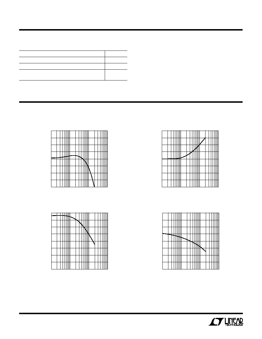
TOTAL DOSE-KRADs (Si)
1
0
INPUT OFFSET VOLTAGE (
µ
V)
500
1000
10
100
1000
1078M ∑ G1
≠500
≠250
250
750
≠750
≠1000
Input Offset Voltage
TOTAL DOSE-KRADs (Si)
1
0
INPUT OFFSET CURRENT (nA)
10
20
10
100
1000
1078M ∑ G2
≠10
≠5
5
15
≠15
≠20
Input Offset Current
Common-Mode Rejection Ratio
TOTAL DOSE-KRADs (Si)
1
110
COMMON-MODE REJECTION RATIO (dB)
120
130
10
100
1000
1078M ∑ G4
100
90
TOTAL DOSE-KRADs (Si)
1
≠80
INPUT BIAS CURRENT (nA)
≠40
0
10
100
1000
1078M ∑ G3
≠120
≠100
≠ 60
≠20
≠140
≠160
Input Bias Current
7
RH1078M
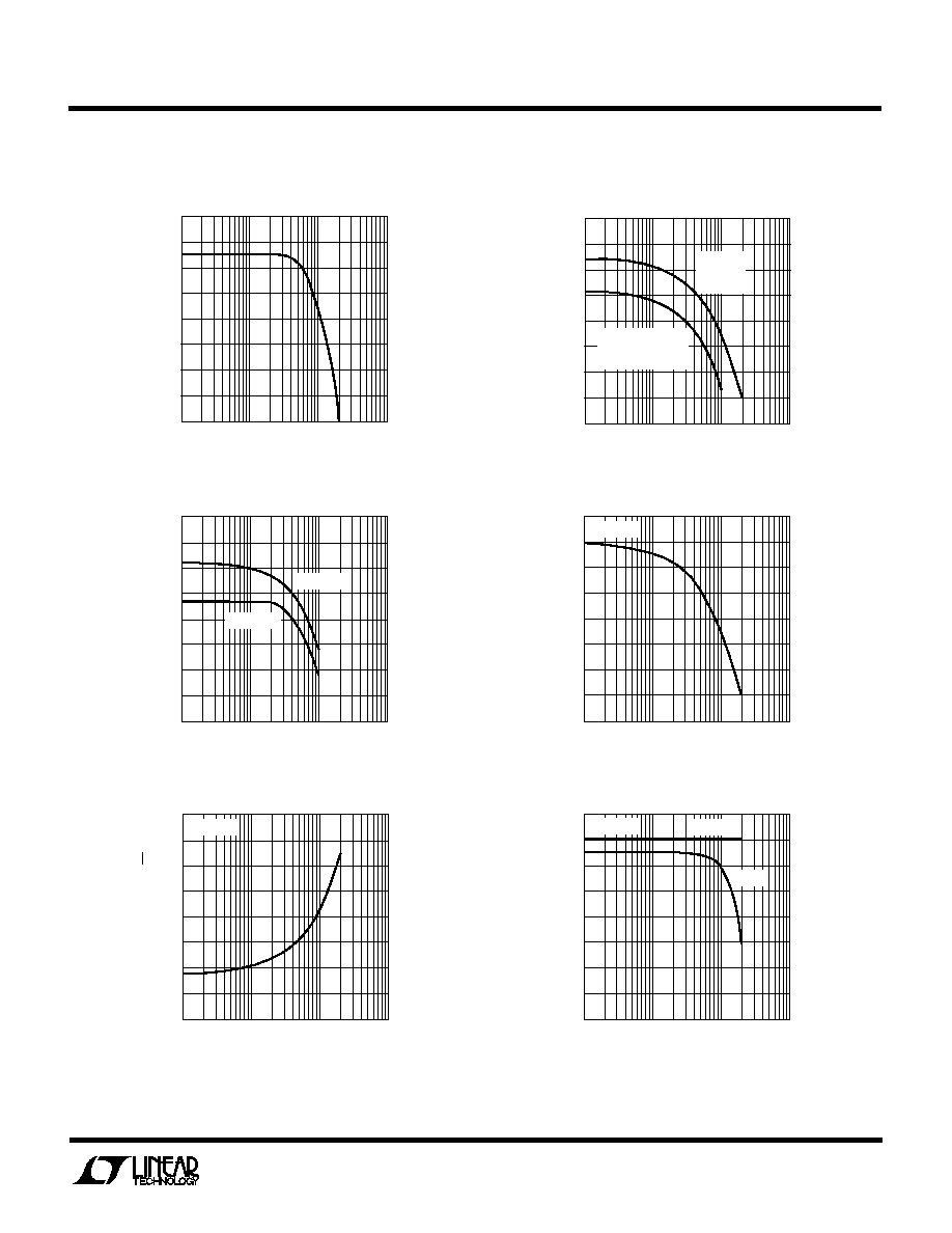
Power Supply Rejection Ratio
TOTAL DOSE-KRADs (Si)
1
100
POWER SUPPLY REJECTION RATIO (dB)
120
140
10
100
1000
1078M ∑ G5
80
90
110
130
70
60
Large-Signal Voltage Gain
TOTAL DOSE-KRADs (Si)
1
110
LARGE-SIGNAL VOLTAGE GAIN (dB)
130
150
10
100
1000
1078M ∑ G6
90
100
120
140
80
70
V
S
= ±15V
V
O
= ±10V
R
L
= 2k
V
S
= 5V, 0V
V
O
= 0.03V TO 3.5V
R
L
= 50k
Slew Rate
TOTAL DOSE-KRADs (Si)
1
0.08
SLEW RATE (V/
µ
s)
0.12
0.16
10
100
1000
1078M ∑ G7
0.04
0.06
0.10
0.14
0.02
0
V
S
= ±15V
V
S
= 5V, 0V
Gain-Bandwidth Product
TOTAL DOSE-KRADs (Si)
1
200
GAIN-BANDWIDTH PRODUCT (kHz)
300
400
10
100
1000
1078M ∑ G8
100
150
250
350
50
0
V
S
= ±15V
10Hz Noise Density
TOTAL DOSE-KRADs (Si)
1
80
10Hz NOISE DENSITY (nV/
Hz)
120
160
10
100
1000
1078M ∑ G9
40
60
100
140
20
0
V
S
= ±15V
Positive Output Voltage Swing
TOTAL DOSE-KRADs (Si)
1
8
POSITIVE OUTPUT VOLTAGE SWING (V)
12
16
10
100
1000
1078M ∑ G10
4
6
10
14
2
0
V
S
= ±15V
R
L
= 50k
R
L
= 2k
TYPICAL APPLICATIO
N
S
U
Information furnished by Linear Technology Corporation is believed to be accurate and reliable.
However, no responsibility is assumed for its use. Linear Technology Corporation makes no represen-
tation that the interconnection of its circuits as described herein will not infringe on existing patent rights.
8
RH1078M
©
LINEAR TECHNOLOGY CORPORATION 1994
rh1078me LT/TP 0798 500 REV E ∑ PRINTED IN USA
I.D. No. 66-10-0100 Rev. E 0798
Linear Technology Corporation
1630 McCarthy Blvd., Milpitas, CA 95035-7417
q
(408) 432-1900
FAX: (408) 434-0507
q
TELEX: 499-3977
q
www.linear-tech.com
TYPICAL APPLICATIO
N
S
U
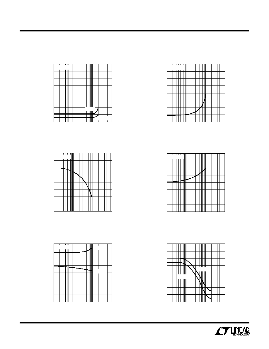
TOTAL DOSE-KRADs (Si)
1
40
SUPPLY CURRENT PER AMPLIFIER (
µ
A)
60
80
10
100
1000
1078M ∑ G16
20
30
50
70
10
0
V
S
= 5V, 0V
V
S
= 15V
Output Voltage Swing Low,
No Load
TOTAL DOSE-KRADs (Si)
1
16
OUTPUT VOLTAGE SWING (mV)
20
26
10
100
1000
1078M ∑ G12
8
12
18
24
4
0
V
S
= 5V, 0V
Negative Output Voltage Swing
TOTAL DOSE-KRADs (Si)
1
≠8
NEGATIVE OUTPUT VOLTAGE SWING (V)
≠4
0
10
100
1000
1078M ∑ G11
≠12
≠10
≠ 6
≠2
≠14
≠16
V
S
= ±15V
R
L
= 50k
R
L
= 2k
Output Voltage Swing Low,
2k to GND
TOTAL DOSE-KRADs (Si)
1
0.8
OUTPUT VOLTAGE SWING (mV)
1.2
1.6
10
100
1000
1078M ∑ G13
0.4
0.6
1.0
1.4
0.2
0
V
S
= 5V, 0V
Output Voltage Swing Low,
I
SINK
= 100mA
TOTAL DOSE-KRADs (Si)
1
80
OUTPUT VOLTAGE SWING (mV)
120
160
10
100
1000
1078M ∑ G14
40
60
100
140
20
0
V
S
= 5V, 0V
Output Voltage Swing High
TOTAL DOSE-KRADs (Si)
1
3.8
OUTPUT VOLTAGE SWING (V)
4.2
4.6
10
100
1000
1078M ∑ G15
3.4
3.6
4.0
4.4
3.2
3.0
V
S
= 5V, 0V
NO LOAD
2k TO GND
Supply Current