
1
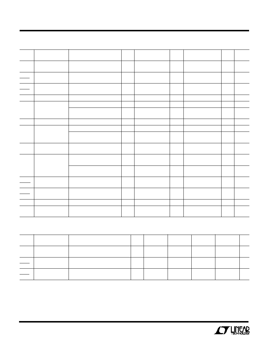
RH117
Positive
Adjustable Regulator
W
U
U
PACKAGE/ORDER I FOR ATIO
BUR -I CIRCUIT
U
U
RH117
V
IN
2k
61.9
ADJ
≠20V
RH117 BI
OUTPUT
20V
BOTTOM VIEW
INPUT
ADJ
OUTPUT
H PACKAGE
3-LEAD TO-39 METAL CAN
1
2
3
2
1
V
IN
CASE
IS OUTPUT
ADJ
K PACKAGE
2-LEAD TO-3 METAL CAN
BOTTOM VIEW
Power Dissipation ............................... Internally Limited
Input-to-Output Voltage Differential ......................... 40V
Operating Junction
Temperature Range ......................... ≠ 55∞C to 150∞C
Storage Temperature Range ................. ≠ 65
∞
C to 150
∞
C
Lead Temperature (Soldering, 10 sec) .................. 300
∞
C
D
U
ESCRIPTIO
A
U
G
W
A
W
U
W
A
R
BSOLUTE
XI
TI
S
The RH117 is a 3-terminal positive adjustable regulator
capable of supplying up to 0.5A (H package) or 1.5A
(K package). The output is adjusted using two external
resistors for a range of 1.2V to 37V. The devices have full
current limit thermal overload safe area protection, all of
which remain functional even if the adjustment terminal is
disconnected.
The wafer lots are processed to LTC's in-house Class S
flow to yield circuits usable in stringent military applica-
tions. In addition to 883 processing, the RH117 is sub-
jected to 100% burn-in in thermal limit.
, LTC and LT are registered trademarks of Linear Technology Corporation.
2
RH117
T
J
= 25∞C
SUB-
SUB-
SYMBOL PARAMETER
CONDITIONS
NOTES
MIN
TYP
MAX
GROUP
MIN
TYP
MAX
GROUP
UNITS
V
REF
Reference Voltage
3V (V
IN
≠ V
OUT
) 40V,
1.20
1.30
1
1.20
1.30
2,3
V
10mA I
OUT
I
MAX
, P P
MAX
V
OUT
Line Regulation
3V (V
IN
≠ V
OUT
) 40V,
2
0.02
1
0.05
2,3
%/V
V
IN
I
OUT
= 10mA
V
OUT
Load Regulation
10mA I
OUT
I
MAX
, V
OUT
5V
2
15
1
50
2,3
mV
I
OUT
10mA I
OUT
I
MAX
, V
OUT
5V
2
0.3
1
1
2,3
%
Thermal Regulation
20ms Pulse
0.07
1
%/W
Ripple Rejection
V
OUT
= 10V, f = 120Hz, C
ADJ
= 0
65
65
dB
V
OUT
= 10V, f = 120Hz,
3
66
66
dB
C
ADJ
= 10µF
I
ADJ
Adjust Pin Current
100
1
100
2,3
µA
I
ADJ
Adjust Pin Current
10mA I
OUT
I
MAX
5
1
5
2,3
µA
Change
2.5V (V
IN
≠ V
OUT
) 40V,
5
1
5
2,3
µA
I
OUT
= 10mA
I
MIN
Minimum Load
(V
IN
≠ V
OUT
) = 40V
5
1
5
2,3
mA
Current
Current Limit
(V
IN
≠ V
OUT
) 15V
H Package
0.5
1
0.5
2,3
A
K Package
1.5
1
1.5
2,3
A
(V
IN
≠ V
OUT
) = 40V H Package
0.15
1
A
K Package
0.30
1
A
V
OUT
Temperature Stability ≠ 55∞C T
J
150∞C
1
%
Temp
V
OUT
Long Term Stability
T
A
= 125∞C
3
1
%
Time
e
n
RMS Output Noise
10Hz f 10kHz
0.001
%
JC
Thermal Resistance
H Package
3
15
∞C/W
(Junction to Case)
K Package
3
3
∞C/W
TABLE 1: ELECTRICAL CHARACTERISTICS
(Preirradiation) (Note 1)
≠ 55∞C T
J
150∞C
SYMBOL
PARAMETER
CONDITIONS
NOTES
MIN
MAX
MIN
MAX
MIN
MAX
MIN
MAX
UNITS
V
REF
Reference Voltage
3V (V
IN
≠ V
OUT
) 40V,
1.20
1.30
1.20
1.30 1.20
1.30
1.20
1.30
V
10mA I
OUT
I
MAX
, P P
MAX
V
OUT
Line Regulation
3V (V
IN
≠ V
OUT
) 40V, I
OUT
= 10mA
2
0.02
0.02
0.02
0.03
%/V
V
IN
V
OUT
Load Regulation
10mA I
OUT
I
MAX
, V
OUT
5V
2
36
42
48
60
mV
I
OUT
10mA I
OUT
I
MAX
, V
OUT
5V
2
0.72
0.84
0.96
1.20
%
TABLE 1A: ELECTRICAL CHARACTERISTICS
(Postirradiation) (Note 4)
100KRAD(Si)
50KRAD(Si)
20KRAD(Si)
10KRAD(Si)

3
RH117
SYMBOL
PARAMETER
CONDITIONS
NOTES
MIN
MAX
MIN
MAX
MIN
MAX
MIN
MAX
UNITS
I
ADJ
Adjust Pin Current
100
100
100
100
µA
I
ADJ
Adjust Pin Current
10mA I
OUT
I
MAX
5
5
5
5
µA
Change
2.5V (V
IN
≠ V
OUT
) 40V,
5
5
5
5
µA
I
OUT
= 10mA
I
MIN
Minimum Load
(V
IN
≠ V
OUT
) = 40V
5
5
5
5
mA
Current
Current Limit
(V
IN
≠ V
OUT
) 15V
H Package
0.5
0.5
0.5
0.5
A
K Package
1.5
1.5
1.5
1.5
A
(V
IN
≠ V
OUT
) = 40V
H Package
0.15
0.15
0.15
0.15
A
K Package
0.30
0.30
0.30
0.30
A
100KRAD(Si)
50KRAD(Si)
20KRAD(Si)
10KRAD(Si)
TABLE 1A: ELECTRICAL CHARACTERISTICS
(Postirradiation) (Note 5)
Note 1: Unless otherwise specified, these specifications apply for
V
IN
≠ V
OUT
= 5V; and I
OUT
= 0.1A for the H package (TO-39) and
I
OUT
= 0.5A for the K package (TO-3) package. Although power dissipation
is internally limited, these specifications are applicable for power
dissipations of 2W for the TO-39 and 20W for the TO-3. I
MAX
is 0.5A for
the TO-39 and 1.5A for the TO-3.
Note 2: Regulation is measured at a constant junction temperature using
pulse testing with a low duty cycle. Changes in output voltage due to
heating effects are covered under the specification for thermal regulation.
Note 3: Guaranteed by design, characterization or correlation to other
tested parameters.
Note 4: T
J
= 25∞C unless otherwise noted.
Information furnished by Linear Technology Corporation is believed to be accurate and reliable.
However, no responsibility is assumed for its use. Linear Technology Corporation makes no represen-
tation that the interconnection of its circuits as described herein will not infringe on existing patent rights.
TOTAL DOSE BIAS CIRCUIT
MIL-STD-883 TEST REQUIREMENTS
SUBGROUP
Final Electrical Test Requirements (Method 5004)
1*,2,3
Group A Test Requirements (Method 5005)
1,2,3
Group C and D End Point Electrical Parameters
1
(Method 5005)
* PDA Applies to subgroup 1. See PDA Test Notes.
PDA Test Notes
The PDA is specified as 5% based on failures from group A, subgroup 1,
tests after cooldown as the final electrical test in accordance with method
5004 of MIL-STD-883 Class B. The verified failures of group A, subgroup
1, after burn-in divided by the total number of devices submitted for burn-
in in that lot shall be used to determine the percent for the lot.
Linear Technology Corporation reserves the right to test to tighter limits
than those given.
TABLE 2: ELECTRICAL TEST REQUIRE E TS
UW
RH117
V
IN
2k
61.9
0.1
µ
F
ADJ
≠15V
RH117 TA01
OUTPUT
15V
4
RH117
Linear Technology Corporation
1630 McCarthy Blvd., Milpitas, CA 95035-7417
(408) 432-1900
q
FAX
: (408) 434-0507
q
TELEX
: 499-3977
©
LINEAR TECHNOLOGY CORPORATION 1989
LT/HP 0796 500 REV B ∑ PRINTED IN USA
I.D. No. 66-11-0117 Rev. B 0796
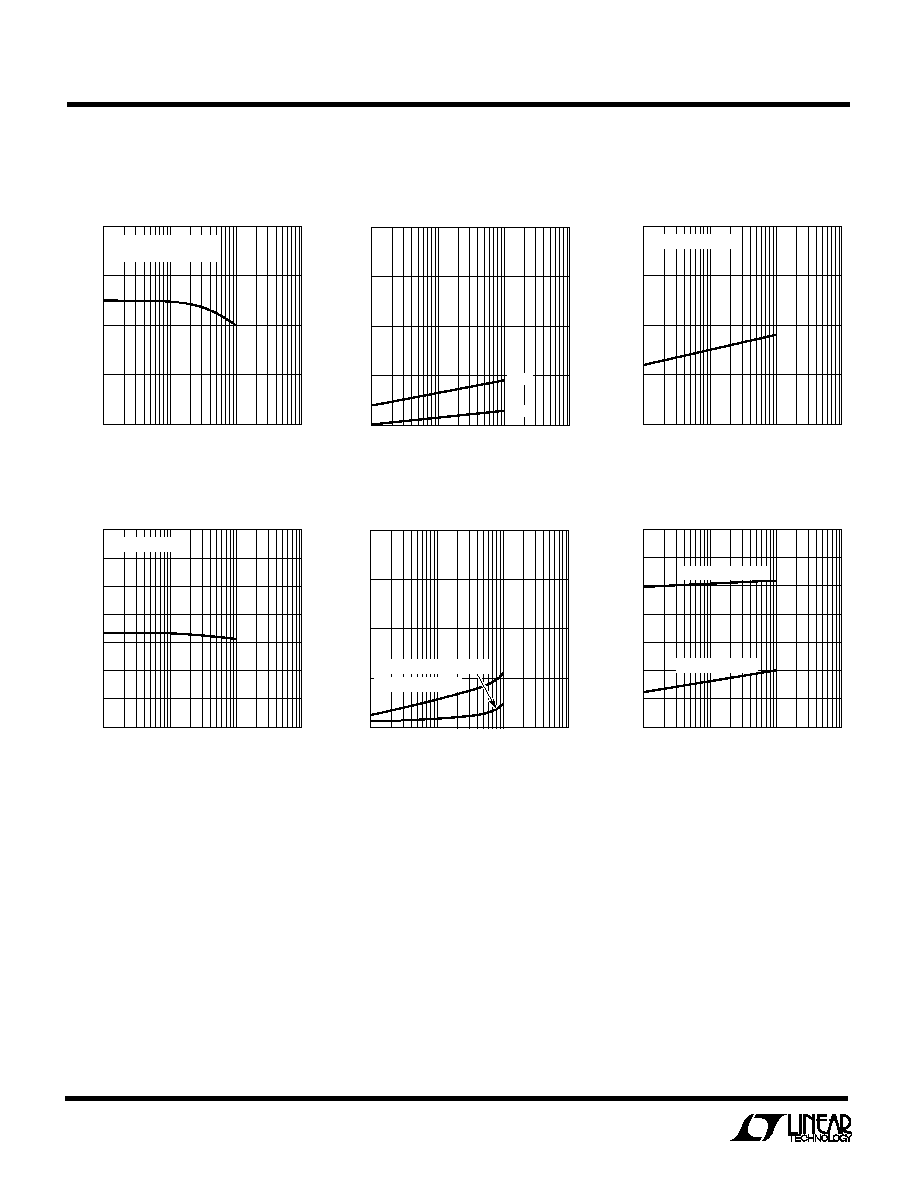
TYPICAL PERFOR
M
A
N
CE CHARACTERISTICS
U
W
Reference Voltage
Regulation
Minimum Load Current
TOTAL DOSE KRAD (Si)
1
REFERENCE VOLTAGE (V)
1.28
1.26
1.24
1.22
1.20
10
100
1000
RH117 G01
3V
(V
IN
≠ V
OUT
)
40V
10mA
I
OUT
I
MAX
TOTAL DOSE KRAD (Si)
1
DIFFERENTIAL REFERENCE VOLTAGE (mV)
20
15
10
5
0
10
100
1000
RH117 G02
LOAD
LINE
TOTAL DOSE KRAD (Si)
1
MINIMUM LOAD CURRENT (mA)
2.0
1.5
1.0
0.5
0
10
100
1000
RH117 G03
(V
IN
≠ V
OUT
) = 13V
Adjust Pin Current
TOTAL DOSE KRAD (Si)
1
ADJUST CURRENT (
µ
A)
55
50
45
40
35
30
25
20
10
100
1000
RH117 G04
(V
IN
≠ V
OUT
) = 3V
Adjust Pin Current Change
TOTAL DOSE KRAD (Si)
1
ADJUST PIN CURRENTCHANGE (
µ
A)
2.0
1.5
1.0
0.5
0
10
100
1000
RH117 G05
2.5V
(V
IN
≠ V
OUT
)
40V
10mA
I
OUT
I
MAX
TOTAL DOSE KRAD (Si)
1
CURRENT LIMIT (A)
3.5
3.0
2.5
2.0
1.5
1.0
0.5
0
10
100
1000
RH117 G06
(V
IN
≠ V
OUT
) = 4.25V
(V
IN
≠ V
OUT
) = 40V
Current Limit