 | –≠–ª–µ–∫—Ç—Ä–æ–Ω–Ω—ã–π –∫–æ–º–ø–æ–Ω–µ–Ω—Ç: 4N27STA-V | –°–∫–∞—á–∞—Ç—å:  PDF PDF  ZIP ZIP |
Document Outline
- ˛ˇ
- ˛ˇ
- ˛ˇ
- ˛ˇ
- ˛ˇ
- ˛ˇ
- ˛ˇ
- ˛ˇ
- ˛ˇ
- ˛ˇ
- ˛ˇ
- ˛ˇ
- ˛ˇ
- ˛ˇ
- ˛ˇ
- ˛ˇ
- ˛ˇ
- ˛ˇ
- ˛ˇ
- ˛ˇ
- ˛ˇ
- ˛ˇ
- ˛ˇ
- ˛ˇ
- ˛ˇ
- ˛ˇ
- ˛ˇ
- ˛ˇ
- ˛ˇ
- ˛ˇ
- ˛ˇ
- ˛ˇ
- ˛ˇ
- ˛ˇ

12-28
General Purpose Type
General Purpose Type
General Purpose Type
General Purpose Type
General Purpose Type
Photocoupler
Photocoupler
Photocoupler
Photocoupler
Photocoupler
LTV-4N25 Series/LTV-4N26 Series
LTV-4N27 Series/LTV-4N28 Series
4N25 Series/4N26 Series/4N27 Series/4N28 Series
Features
Response Time
(tr : TYP,3
s at V
CE
=10V, I
C
=2mA, R
L
=100
)
UL approved (No. E113898)
TUV approved (No.R9653630)
CSA approved (No. CA91533-1)
FIMKO approved (No. 193422)
NEMKO approved (No. P96103013)
DEMKO approved (No. 303985)
SEMKO approved (No. 9646047/01-30)
VDE approved (No. 094722 )
Options available :
-Leads with 0.4"(10.16mm)spacing (M Type)
-Leads bends for surface mounting(S Type)
-Tape and Reel of Type I for SMD(Add"-TA"Suffix)
-Tape and Reel of Type II for SMD(Add"-TA1"Suffix)
-VDE 0884 approvals (Add"-V"Suffix)
Applications
1. I/O interfaces for computers.
2. System appliances, measuring instruments.
3. Signal transmission between circuits of different poten-
tials and impedances.
Note:
1.Year date code.
2. 2-digit work week.
3. Factory code shall be marked (Z : Taiwan, Y : Thailand).
4. Model No. : LTV4N25 ; LTV4N26 ; LTV4N27 ; LTV4N28
; 4N25 ; 4N26 ; 4N27 ; 4N28.
5. All dimensions are in millimeters (inches).
6. Tolerance is
0.25mm (.010 ) unless otherwise noted.
7. Specifications are subject to change without notice.
Package Dimensions
12-29
PHO
T
OCOUPLER
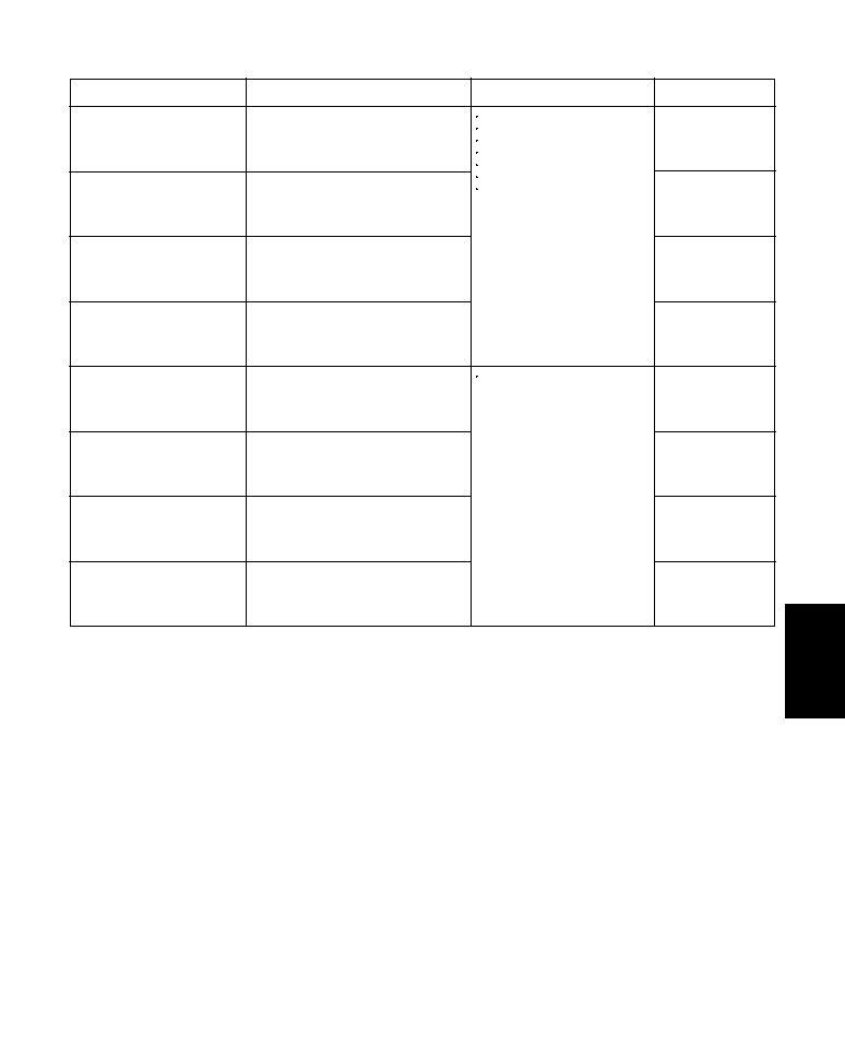
Ordering Information
Part Number
Package
Safety Standard Approval
Application part
number
LTV-4N25 / 4N25
LTV-4N25M / 4N25M
LTV-4N25S / 4N25S
LTV-4N25S-TA / 4N25S-TA
LTV-4N25S-TA1 / 4N25S-TA1
LTV-4N26 / 4N26
LTV-4N26M / 4N26M
LTV-4N26S / 4N26S
LTV-4N26S-TA / 4N26S-TA
LTV-4N26S-TA1 / 4N26S-TA1
LTV-4N27 / 4N27
LTV-4N27M / 4N27M
LTV-4N27S / 4N27S
LTV-4N27S-TA / 4N27S-TA
LTV-4N27S-TA1 / 4N27S-TA1
LTV-4N28 / 4N28
LTV-4N28M / 4N28M
LTV-4N28S / 4N28S
LTV-4N28S-TA / 4N28S-TA
LTV-4N28S-TA1 / 4N28S-TA1
LTV4N25-V / 4N25-V
LTV4N25M-V / 4N25M-V
LTV4N25S-V / 4N25S-V
LTV4N25STA-V / 4N25STA-V
LTV4N25STA1-V / 4N25STA1-V
LTV4N26-V / 4N26-V
LTV4N26M-V / 4N26M-V
LTV4N26S-V / 4N26S-V
LTV4N26STA-V / 4N26STA-V
LTV4N26STA1-V / 4N26STA1-V
LTV4N27-V / 4N27-V
LTV4N27M-V / 4N27M-V
LTV4N27S-V / 4N27S-V
LTV4N27STA-V / 4N27STA-V
LTV4N27STA1-V / 4N27STA1-V
LTV4N28-V / 4N28-V
LTV4N28M-V / 4N28M-V
LTV4N28S-V / 4N28S-V
LTV4N28STA-V / 4N28STA-V
LTV4N28STA1-V / 4N28STA1-V
6-pin DIP
6-pin (leads with 0.4" spacing)
6-pin (lead bends for surface mount)
6-pin (tape and reel packaging of type I)
6-pin (tape and reel packaging of type II)
6-pin DIP
6-pin (leads with 0.4" spacing)
6-pin (lead bends for surface mount)
6-pin (tape and reel packaging of type I)
6-pin (tape and reel packaging of type II)
6-pin DIP
6-pin (leads with 0.4" spacing)
6-pin (lead bends for surface mount)
6-pin (tape and reel packaging of type I)
6-pin (tape and reel packaging of type II)
6-pin DIP
6-pin (leads with 0.4" spacing)
6-pin (lead bends for surface mount)
6-pin (tape and reel packaging of type I)
6-pin (tape and reel packaging of type II)
6-pin DIP
6-pin (leads with 0.4" spacing)
6-pin (lead bends for surface mount)
6-pin (tape and reel packaging of type I)
6-pin (tape and reel packaging of type II)
6-pin DIP
6-pin (leads with 0.4" spacing)
6-pin (lead bends for surface mount)
6-pin (tape and reel packaging of type I)
6-pin (tape and reel packaging of type II)
6-pin DIP
6-pin (leads with 0.4" spacing)
6-pin (lead bends for surface mount)
6-pin (tape and reel packaging of type I)
6-pin (tape and reel packaging of type II)
6-pin DIP
6-pin (leads with 0.4" spacing)
6-pin (lead bends for surface mount)
6-pin (tape and reel packaging of type I)
6-pin (tape and reel packaging of type II)
UL approved
TUV approved
CSA approved
FIMKO approved
NEMKO approved
SEMKO approved
DEMKO approved
VDE approved
LTV - 4N25
LTV - 4N26
LTV - 4N27
LTV - 4N28
LTV - 4N25
LTV - 4N26
LTV - 4N27
LTV - 4N28
12-30
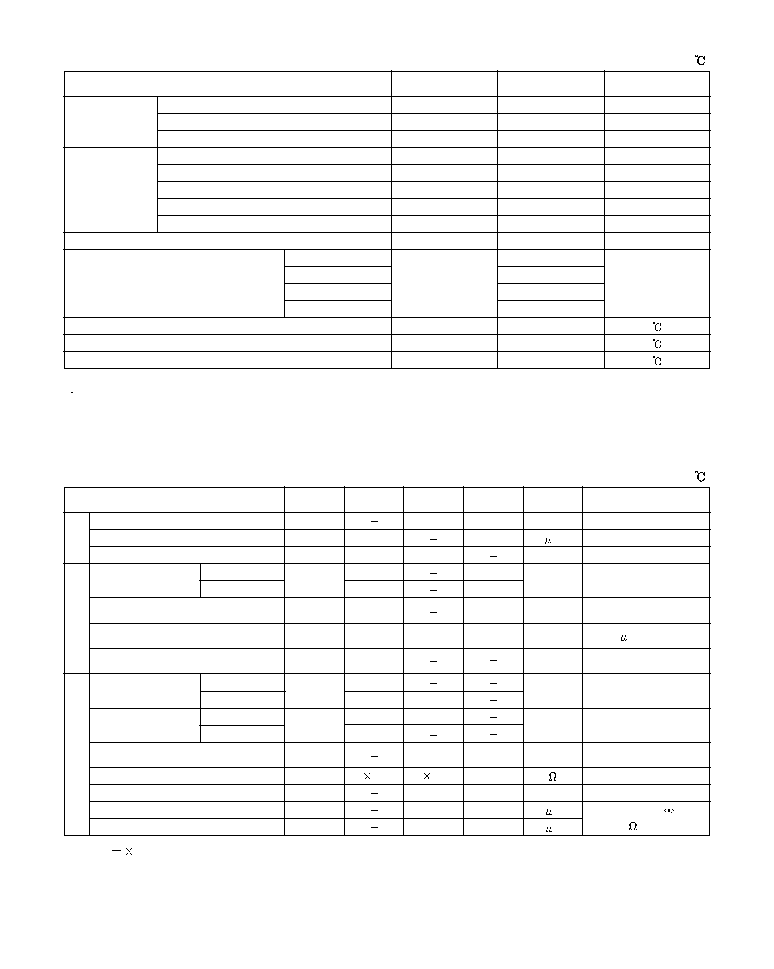
Absolute Maximum Ratings
(Ta=25
)
Parameter
Symbol Rating Unit
Input
Output
Total Power Dissipation
*1.Isolation Voltage
Operating Temperature
Storage Temperature
*2.Soldering Temperature
Forward Current
Reverse Voltage
Power Dissipation
Collector-Emitter Voltage
Collector-Base Voltage
Emitter-Collector Voltage
Collector Current
Collector Power Dissipation
4N25
4N26
4N27
4N28
I
F
V
R
P
V
CEO
V
CBO
V
ECO
I
C
P
C
P
tot
V
iso
T
opr
T
stg
T
sol
80
6
150
30
70
7
100
150
250
2,500
1,500
1,500
500
-55~+100
-55~+150
260
mA
V
mW
V
V
V
mA
mW
mW
V
rms
*1. AC for 1 minute, R.H. = 40 ~ 60%
Isolation voltage shall be measured using the following method.
(1)Short between anode and cathode on the primary side and between collector, emitter and base on the secondary side.
(2)The isolation voltage tester with zero-cross circuit shall be used.
(3)The waveform of applied volttage shall be a sine wave.
*2. For 10 seconds.
Electrical/Optical Characteristics
(Ta=25
)
Parameter Symbol Min. Typ. Max. Unit Conditions
Input
Output
Transfer
Characteristics
Forward Voltage
Reverse Current
Terminal Capacitance
Collector
Dark Current
Collector-Emitter
Breakdown Voltage
Emitter-Collector
Breakdown Voltage
Collector-Base
Breakdown Voltage
Collector
Current
*1 Current
Transfer Ratio
Collector-emitter
Saturation Voltage
Isolation Resistance
Floating Capacitance
Response Time (Rise)
Response Time (Fall)
4N25/26/27
4N28
4N25/26
4N27/28
4N25/26
4N27/28
V
F
I
R
C
t
I
CEO
BV
CEO
BV
ECO
BV
CBO
I
C
CTR
V
CE(sat)
R
ISO
C
f
t
r
t
f
30
7
70
2
1
20
10
5
10
10
1.2
50
0.1
1
10
11
1.0
3
3
1.5
10
50
100
0.5
V
A
pF
nA
V
V
V
mA
%
V
pF
s
s
I
F
=10mA
V
R
=4V
V=0, f=1kHz
V
CE
=10V
I
C
=0.1mA
I
E
=10
A
I
C
=0.1mA
*1. CTR=
100%
I
C
I
F
I
F
=10mA
V
CE
=10V
I
F
=10mA
V
CE
=10V
I
F
=50mA, I
C
=2mA
DC500V, 40~60% R.H.
V=0, f=1MHz
V
CE
=10V, R
BE
=
R
L
=100
, I
C
=2mA

12-31
PHO
T
OCOUPLER
Typical Electrical/Optical Characteristic Curves
(25
Ambient Temperature Unless Otherwise Noted)

12-32