
1
LTC1731-8.2/LTC1731-8.4
sn1731 17318fs
FEATURES
APPLICATIO S
U
DESCRIPTIO
U
TYPICAL APPLICATIO
U
Lithium-Ion Linear
Battery Charger Controller
The LTC
Æ
1731-8.2/LTC1731-8.4 are complete constant-
current/constant-voltage linear charger controllers for 2-
cell lithium-ion (Li-Ion)batteries. Nickel-cadmium (NiCd)
and nickel-metal-hydride (NiMH) batteries can also be
charged with constant current using external termina-
tion. The external sense resistor sets the charge current
with 7% accuracy. An internal resistor divider and preci-
sion reference set the final float potential with 1% accu-
racy. The output float voltages are set internally to 8.2V
(LTC1731-8.2) or 8.4V (LTC1731-8.4).
When the input supply is removed, the LTC1731-8.2/
LTC1731-8.4 automatically enter a low current sleep mode,
dropping the battery drain current to typically 15
µ
A. An
internal comparator detects the end-of-charge (C/10) con-
dition while a programmable timer, using an external
capacitor, sets the total charge time. Fully discharged cells
are automatically trickle charged at 10% of the pro-
grammed current until battery voltage exceeds 4.95V.
The LTC1731-8.2/LTC1731-8.4 are available in the 8-pin
MSOP and SO packages. For 1-cell Li-Ion battery charg-
ing, see the LTC1731-4.1 and LTC1731-4.2 data sheets.
s
Complete Linear Charger Controller for
2-Cell Lithium-Ion Batteries
s
1% Voltage Accuracy
s
Programmable Charge Current
s
C/10 Charge Current Detection Output
s
Programmable Charge Termination Timer
s
Space Saving 8-Pin MSOP Package
s
Automatic Sleep Mode When Input Supply
is Removed (15
µ
A Battery Drain)
s
Automatic Trickle Charging of Low Voltage Cells
s
Programmable for Constant-Current-Only Mode
s
Cellular Phones
s
Handheld Computers
s
Charging Docks and Cradles
s
Programmable Current Source
, LTC and LT are registered trademarks of Linear Technology Corporation.
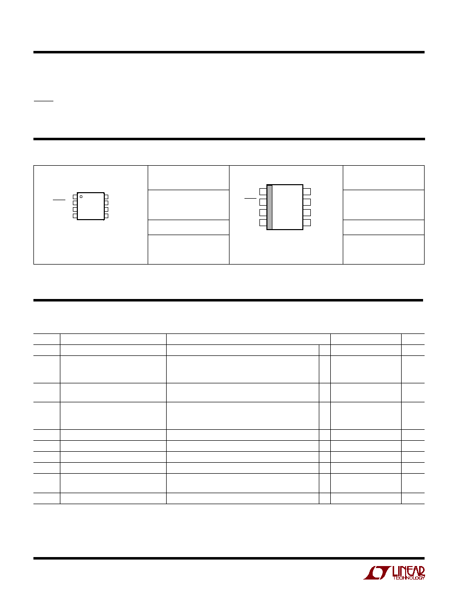
400mA Li-Ion Charger
V
CC
V
IN
= 9V
SENSE
DRV
2k
R
SENSE
0.2
R
PROG
*
19.6k
2-CELL
Li-ION
LTC1731-8.4
*SHUTDOWN INVOKED BY FLOATING THE PROG PIN
BAT
CHRG
8
7
MBRM120T3
10
µ
F
1731 TA01
1
µ
F
I
BAT
= 400mA
C
TIMER
0.1
µ
F
Q1
Si9430DY
6
1
5
4
2
3
TIMER
PROG
GND
+
CHARGE
STATUS
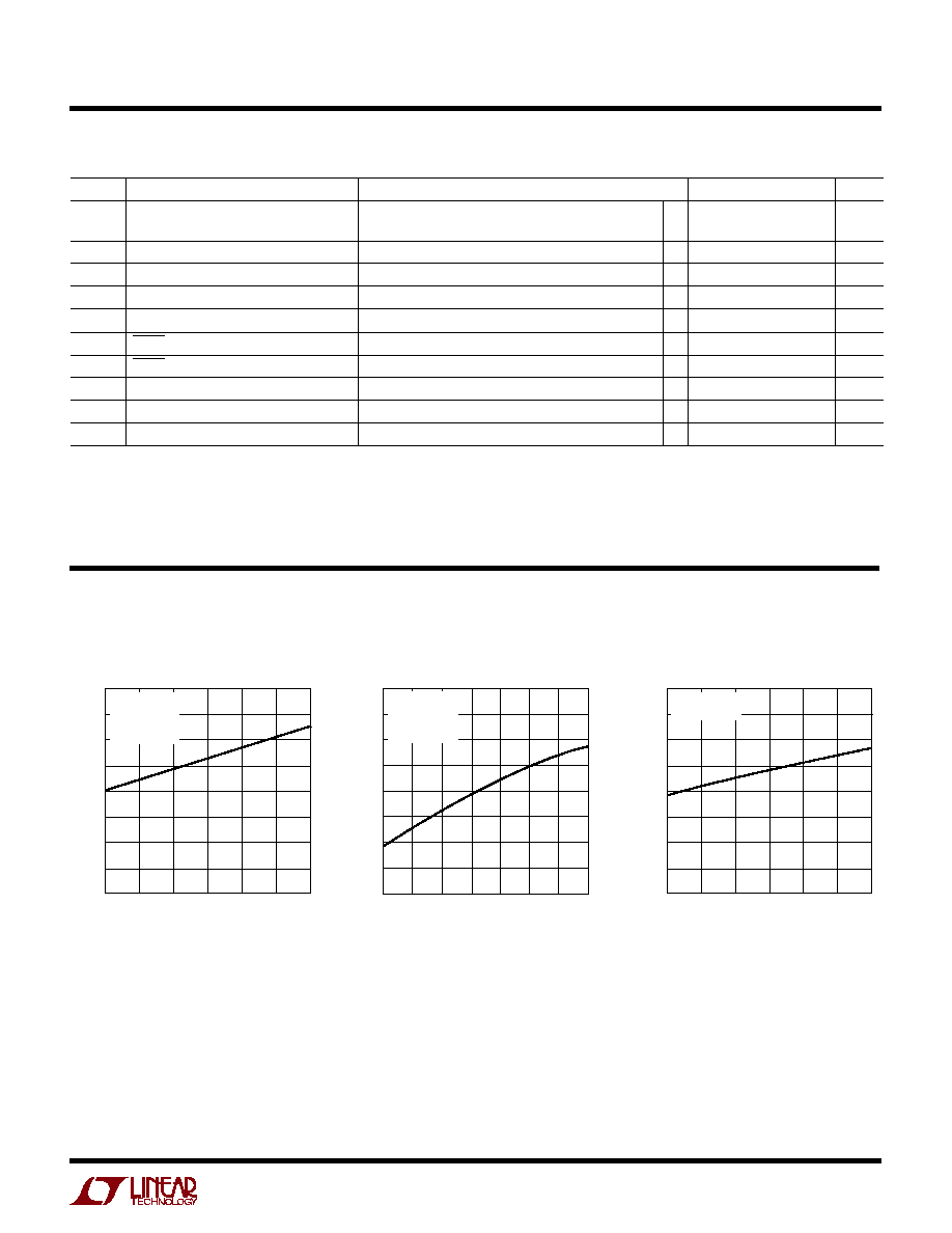
Typical Li-Ion Charge Cycle
TIME (HOURS)
0
CHARGE CURRENT (mA)
400
300
200
100
0
9
8
7
6
1.5
2.5
1731 TA01b
0.5
1.0
2.0
3.0
CONSTANT
VOLTAGE
CONSTANT
CURRENT
TIMER
STOPS
CHRG
LED OFF
BATTERY VOLTAGE
400mA HR BATTERY
CHARGE CURRENT
BATTERY VOLTAGE(V)
2
LTC1731-8.2/LTC1731-8.4
sn1731 17318fs
SYMBOL
PARAMETER
CONDITIONS
MIN
TYP
MAX
UNITS
V
CC
Input Supply Voltage
q
8.8
12
V
I
CC
Input Supply Current
Charger On, Current Mode
q
1
3
mA
Shutdown Mode
q
1
2
mA
Sleep Mode (Battery Drain Current)
15
30
µ
A
V
BAT
Regulated Output Voltage
LTC1731-8.2 (9V
V
CC
12V)
q
8.118
8.2
8.282
V
LTC1731-8.4 (9V
V
CC
12V)
q
8.316
8.4
8.484
V
I
BAT
Current Mode Charge Current
R
PROG
= 19.6k, R
SENSE
= 0.2
465
500
535
mA
R
PROG
= 19.6k, R
SENSE
= 0.2
q
415
500
585
mA
R
PROG
= 97.6k, R
SENSE
= 0.2
70
100
130
mA
I
TRIKL
Trickle Charge Current
V
BAT
= 4V, R
PROG
= 19.6k, I
TRIKL
= (V
CC
≠ V
SENSE
)/0.2
q
30
50
100
mA
V
TRIKL
Trickle Charge Threshold Voltage
BAT Rising
q
4.7
4.95
5.1
V
V
UV
V
CC
Undervoltage Lockout Voltage
V
CC
Rising
q
8.2
8.8
V
V
UV
V
CC
Undervoltage Lockout Hysteresis
V
CC
Falling
200
mV
V
MSD
Manual Shutdown Threshold Voltage
PROG Pin Rising
2.457
V
PROG Pin Falling
2.446
V
I
DRV
Drive Pin Current
V
DRV
= V
CC
≠ 2V
26
µ
A
ORDER PART
NUMBER
(Note 1)
Input Supply Voltage (V
CC
) ................................... 13.2V
SENSE, DRV, BAT, TIMER, PROG ............ ≠ 0.3V to V
CC
CHRG ..................................................... ≠ 0.3V to 13.2V
LTC1731EMS8-8.2
LTC1731EMS8-8.4
T
JMAX
= 150
∞
C,
JA
= 200
∞
C/W
Consult LTC Marketing for parts specified with wider operating temperature ranges.
ABSOLUTE
M
AXI
M
U
M
RATINGS
W
W
W
U
PACKAGE/ORDER I
N
FOR
M
ATIO
N
W
U
U
Operating Temperature Range (Note 2) .....≠ 40
∞
to 85
∞
C
Storage Temperature Range ................. ≠ 65
∞
C to 150
∞
C
Lead Temperature (Soldering, 10 sec).................. 300
∞
C
MS8 PART MARKING
LTSW
LTPE
1
2
3
4
BAT
CHRG
TIMER
GND
8
7
6
5
SENSE
V
CC
DRV
PROG
TOP VIEW
MS8 PACKAGE
8-LEAD PLASTIC MSOP
ORDER PART
NUMBER
LTC1731ES8-8.2
LTC1731ES8-8.4
S8 PART MARKING
173182
173184
The
q
denotes the specifications which apply over the full operating
temperature range, otherwise specifications are at T
A
= 25
∞
C. V
CC
= 9V unless otherwise noted.
ELECTRICAL CHARACTERISTICS
1
2
3
4
8
7
6
5
TOP VIEW
SENSE
V
CC
DRV
PROG
BAT
CHRG
TIMER
GND
S8 PACKAGE
8-LEAD PLASTIC SO
T
JMAX
= 150
∞
C,
JA
= 125
∞
C/W
3
LTC1731-8.2/LTC1731-8.4
sn1731 17318fs
Note 1: Absolute Maximum Ratings are those values beyond which the life
of a device may be impaired.
SYMBOL
PARAMETER
CONDITIONS
MIN
TYP
MAX
UNITS
V
ASD
Automatic Shutdown Threshold Voltage
(V
CC
≠ V
BAT
) Falling
30
54
90
mV
(V
CC
≠ V
BAT
) Rising
40
69
100
mV
V
DIS
Voltage Mode Disable Threshold Voltage
V
DIS
=
(V
CC
≠ V
TIMER
)
q
0.4
V
I
PROG
PROG Pin Current
Internal Pull-Up Current, No R
PROG
2.5
µ
A
PROG Pin Load Regulation
PROG Pin Source Current,
V
PROG
5mV
q
300
µ
A
V
PROG
PROG Pin Voltage
R
PROG
=19.6k
2.457
V
I
CHRG
CHRG Pin Weak Pull-Down Current
V
CHRG
= 1V
50
100
150
µ
A
V
CHRG
CHRG Pin Output Low Voltage
I
CHRG
= 5mA
0.6
1.2
V
I
C/10
End of Charge Indication Current Level
R
PROG
= 19.6k, R
SENSE
= 0.2
q
25
50
100
mA
t
TIMER
TIMER Accuracy
C
TIMER
= 0.01
µ
F
10
%
V
CLAMP
DRV Pin Clamp Voltage
V
CLAMP
= V
CC
≠ V
DRV
, I
DRIVE
= 50
µ
A
6.5
V
ELECTRICAL CHARACTERISTICS
Note 2: The LTC1731E-8.2/LTC1731E-8.4 are guaranteed to meet
performance specifications from 0
∞
C to 70
∞
C. Specifications over the
≠ 40
∞
C to 85
∞
C operating temperature range are assured by design,
characterization and correlation with statistical process controls. Consult
factory for I grade parts.
The
q
denotes the specifications which apply over the full operating
temperature range, otherwise specifications are at T
A
= 25
∞
C. V
CC
= 9V unless otherwise noted.
TYPICAL PERFOR A CE CHARACTERISTICS
U
W
V
CC
(V)
9
I
TRKL
(mA)
10
11
12
1731 G01
60
55
50
45
40
R
PROG
= 19.6K
R
SENSE
= 0.2
V
BAT
= 4V
T
A
= 25
∞
Trickle Charge Current
vs V
CC
I
TRKL
(mA)
60
55
50
45
40
TEMPERATURE (
∞
C)
≠50
100
1731 G06
0
50
≠25
25
75
125
R
PROG
= 19.6K
R
SENSE
= 0.2
V
BAT
= 4V
V
CC
= 9V
V
CC
(V)
9
V
TRKL
(V)
10
11
12
1731 G08
4.96
4.95
4.94
4.93
4.92
4.91
4.90
4.89
4.88
R
PROG
= 19.6K
T
A
= 25
∞
Trickle Charge Current
vs Temperature
Trickle Charge Threshold Voltage
vs V
CC
4
LTC1731-8.2/LTC1731-8.4
sn1731 17318fs
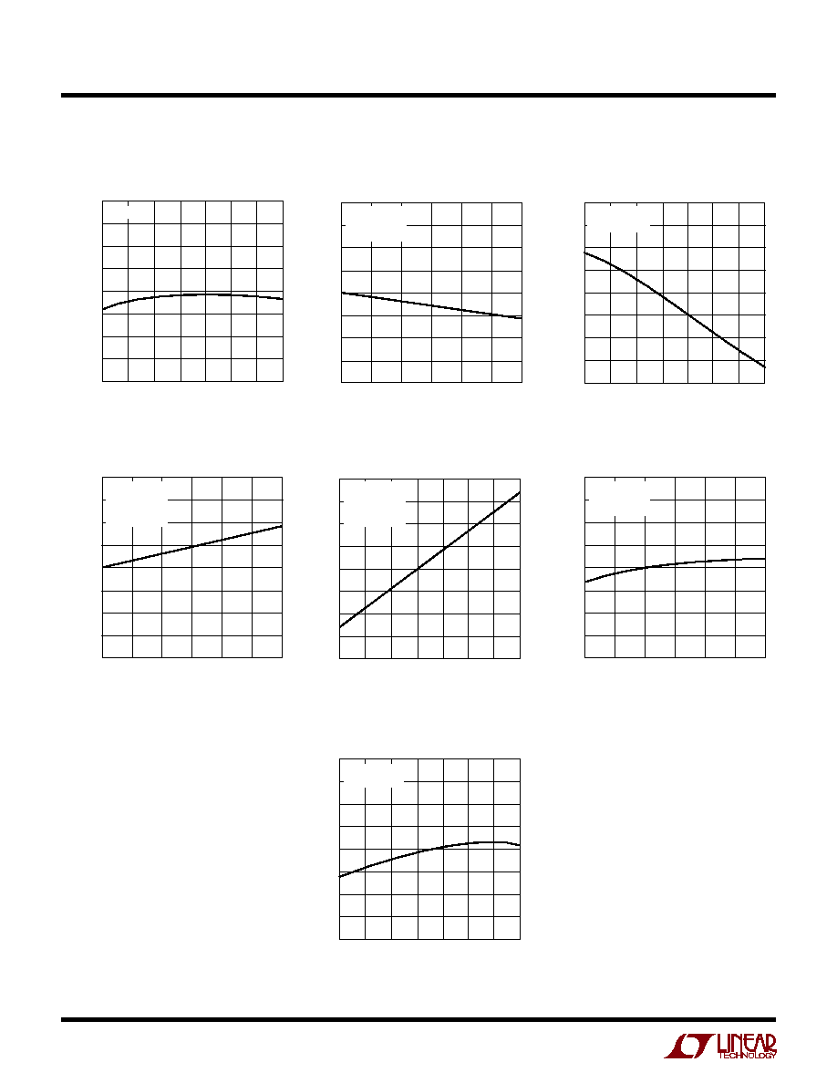
TYPICAL PERFOR A CE CHARACTERISTICS
U
W
TEMPERATURE (
∞
C)
≠50
t
TIMER
(%)
100
1731 G04
0
50
110
105
100
95
90
≠25
25
75
125
C
TIMER
= 0.1
µ
F
V
CC
= 9V
V
CC
(V)
9
t
TIMER
(%)
10
11
12
1731 G05
110
105
100
95
90
C
TIMER
= 0.1
µ
F
V
BAT
= 6V
T
A
= 25
∞
V
CC
(V)
9
I
BAT
(mA)
10
11
12
1731 G09
520
510
500
490
480
R
PROG
= 19.6K
R
SENSE
= 0.2
V
BAT
= 6V
T
A
= 25
∞
V
CC
(V)
9
V
PROG
(V)
10
11
12
1731 G10
2.48
2.47
2.46
2.45
2.44
R
PROG
= 19.6K
V
BAT
= 6V
T
A
= 25
∞
Timer Accuracy vs Temperature
Timer Accuracy vs V
CC
Battery Charge Current
vs Temperature
Battery Charge Current
vs V
CC
Program Pin Voltage
vs V
CC
I
BAT
(mA)
540
530
520
510
500
490
480
470
460
TEMPERATURE (
∞
C)
≠50
100
1731 G07
0
50
≠25
25
75
125
R
PROG
= 19.6K
R
SENSE
= 0.2
V
BAT
= 6V
V
CC
= 9V
TEMPERATURE (
∞
C)
≠50
V
PROG
(V)
100
1731 G02
0
50
2.470
2.465
2.460
2.455
2.450
≠25
25
75
125
R
PROG
= 19.6k
V
CC
= 9V
TEMPERATURE (
∞
C)
≠50
V
TRKL
(V)
100
1731 G03
0
50
4.94
4.93
4.92
4.91
4.90
≠25
25
75
125
V
CC
= 9V
Trickle Charge Threshold Voltage
vs Temperature
Program Pin Voltage
vs Temperature

5
LTC1731-8.2/LTC1731-8.4
sn1731 17318fs
PI
N
FU
N
CTIO
N
S
U
U
U
BAT (Pin 1): Battery Sense Input. A bypass capacitor of at
least 10
µ
F is required to keep the loop stable when the
battery is not connected. A precision internal resistive
divider sets the final float potential on this pin. The resistor
divider is disconnected in sleep mode.
CHRG (Pin 2): Open-Drain Charge Status Output. When
the battery is being charged, the CHRG pin is pulled low by
an internal N-channel MOSFET. When the charge current
drops to 10% of the full-scale current for at least 0.32
seconds, the N-channel MOSFET turns off and a 100
µ
A
current source is connected from the CHRG pin to GND.
When the timer runs out or the input supply is removed,
the current source will be disconnected and the CHRG pin
is forced into a high impedance state.
TIMER (Pin 3): Timer Capacitor and Constant-Voltage
Mode Disable Input Pin. A capacitor C
TIMER
connected
from this pin to ground sets a 30 hour/
µ
F time period for
charge termination. When the TIMER pin is connected to
V
CC
, the constant-voltage mode and the timer is disabled
and the IC will operate in constant-current mode only.
Short the TIMER pin to GND to disable the internal timer
and the C/10 functions.
GND (Pin 4): Ground.
PROG (Pin 5): Charge Current Program and Shutdown
Input Pin. The charge current is programmed by connect-
ing a resistor, R
PROG
to ground. The charge current is I
BAT
= (V
PROG
∑ 800
)/(R
PROG
∑ R
SENSE
). The IC can be forced
into shutdown by floating the PROG pin and allowing the
internal 2.5
µ
A current source to pull the pin above the
2.457V shutdown threshold voltage.
DRV (Pin 6): Drive Output Pin for the P-Channel MOSFET
or PNP Transistor. If a PNP transistor is used, it must have
high gain (see Applications Information section). The DRV
pin is internally clamped to 6.5V below V
CC
.
V
CC
(Pin 7): Input Supply Voltage. V
CC
ranges from 8.8V
to 12V when charging. If V
CC
drops below V
BAT
+ 54mV,
for example when the input supply is disconnected, then
the IC enters sleep mode with I
CC
< 30
µ
A. Bypass this pin
with a 1
µ
F capacitor.
SENSE (Pin 8): Current Sense Input. Connect this pin to
the sense resistor. Choose the resistor value using the
following equation:
R
SENSE
= (V
PROG
∑ 800
)/(R
PROG
∑ I
BAT
)