 | –≠–ª–µ–∫—Ç—Ä–æ–Ω–Ω—ã–π –∫–æ–º–ø–æ–Ω–µ–Ω—Ç: LTW-2S3D7 | –°–∫–∞—á–∞—Ç—å:  PDF PDF  ZIP ZIP |
LITE-ON TECHNOLOGY CORPORATION
P r o p e r t y o f L i t e - O n O n l y
Features
* Low power consumption.
* High efficiency.
* Versatile mounting on p.c. board or panel.
* I.C. compatible/low current requirement.
* Popular T-1
3/4
diameter.
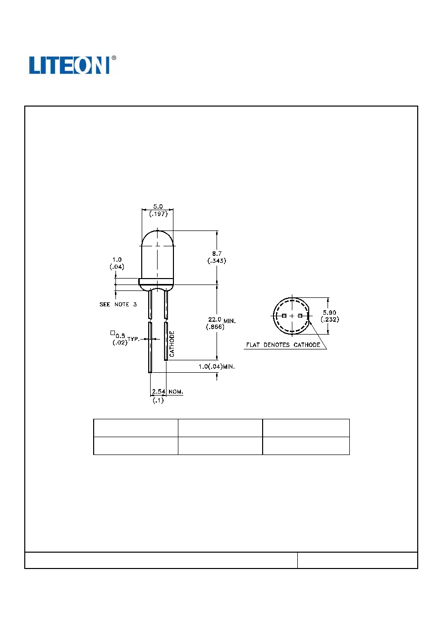
Package Dimensions
Part No.
Lens Color
Emitted Color
LTW-2S3D7
Water Clear
InGaN White
NOTES:
1. All dimensions are in millimeters (inches).
2. Tolerance is ±0.25mm(.010") unless otherwise noted.
3. Protruded resin under flange is 1.0mm(.04") max.
4. Lead spacing is measured where the leads emerge from the package.
5. Specifications are subject to change without notice.
Part No. : LTW-2S3D7
Page : 1 of 8
BNS-OD-C131/A4
LITE-ON TECHNOLOGY CORPORATION
P r o p e r t y o f L i t e - O n O n l y
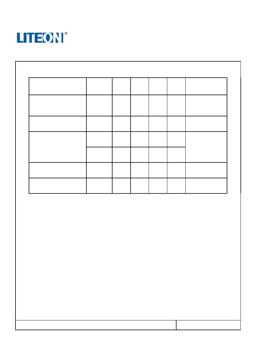
Absolute Maximum Ratings at T
a
=25
PARAMETER
MAXIMUM
RATING
UNIT
Power
Dissipation
120
mW
Peak Forward Current
(1/10 Duty Cycle, 0.1ms Pulse Width)
100 mA
DC Forward Current
30
mA
Reverse
Voltage
5
V
Operating Temperature Range
-25 to + 80
Storage Temperature Range
-30 to + 100
Lead Soldering Temperature
[1.6mm(.063") From Body]
260 for 5 Seconds
Part No. : LTW-2S3D7
Page : 2 of 8
BNS-OD-C131/A4
LITE-ON TECHNOLOGY CORPORATION
P r o p e r t y o f L i t e - O n O n l y
Electrical / Optical Characteristics at Ta=25
PARAMETER SYMBOL
MIN.
TYP.
MAX.
UNIT
TEST
CONDITION
Luminous
Intensity
Iv 10000
13000
mcd
I
F
= 20mA
Note 1,2,3
Iv Spec. Table
Viewing
Angle
2
1/2
15 deg Note
4
x
0.30
Chromaticity Coordinates
y
0.30
I
F
= 20mA
Note 5
Hue Spec. Table &
Chromaticity Diagram
Forward
Voltage
V
F
3.3
3.8
V I
F
= 20mA
Reverse
Current
I
R
100
A
V
R
= 5V
NOTE: 1. Luminous intensity is measured with a light sensor and filter combination that approximates the CIE
eye-response curve.
2. The Iv guarantee should be added ±15tolerance.
3. Iv classification code is marked on each packing bag.
4.
1/2
is the off-axis angle at which the luminous intensity is half the axial luminous intensity.
5. The chromaticity coordinates (x, y) is derived from the 1931 CIE chromaticity diagram.
6. Precautions in handling:
When soldering, leave 2mm of minimum clearance from the resin to the soldering point.
Dipping the resin to solder must be avoided.
Correcting the soldered position after soldering must be avoided.
In soldering, do not apply any stress to the lead frame particularly when heated.
Lead forming must be done before soldering.
It is necessary to cut the lead frame at normal temperature.
7. Caution in ESD:
Static Electricity and surge damages the LED. It is recommend to use a wrist band or
anti-electrostatic glove when handling the LED. All devices, equipment and machinery
must be properly grounded.
Part No. : LTW-2S3D7
Page : 3 of 8
BNS-OD-C131/A4
LITE-ON TECHNOLOGY CORPORATION
P r o p e r t y o f L i t e - O n O n l y
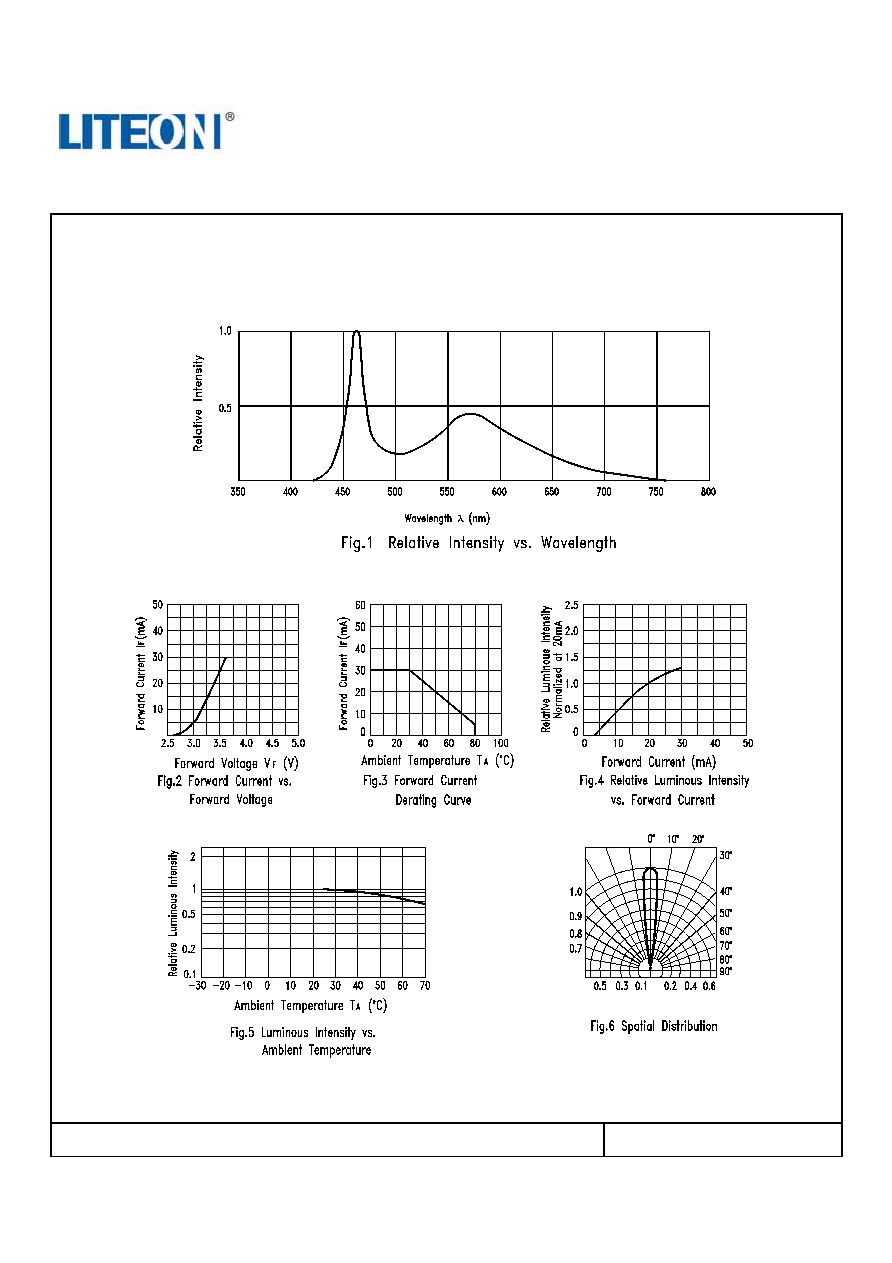
Typical Electrical / Optical Characteristics Curves
(25 Ambient Temperature Unless Otherwise Noted)
Part No. : LTW-2S3D7
Page : 4 of 8
BNS-OD-C131/A4
LITE-ON TECHNOLOGY CORPORATION
P r o p e r t y o f L i t e - O n O n l y
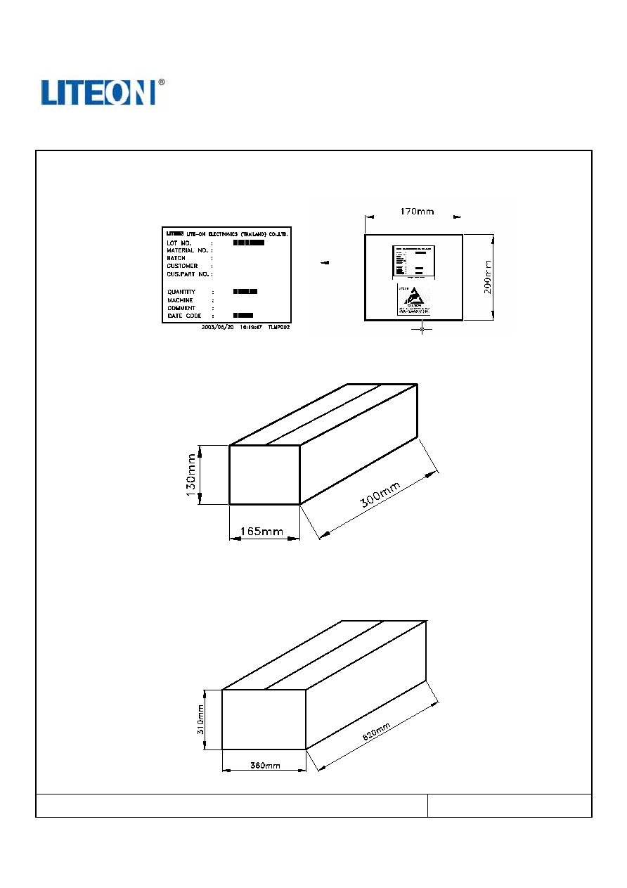
Packing Spec
500 or 250 pcs per packing bag
10 packing bags per inner carton
Total 5,000 pcs per inner carton
8 Inner cartons per outer carton
Total 40,000 pcs per outer carton
Part No. : LTW-2S3D7
Page : 5 of 8
BNS-OD-C131/A4