
52
w w w . l i t t e l f u s e . c o m
CRxxxx series
Description
The CR range of protectors are based on the proven
technology of the T10 thyristor product. Designed for
transient voltage protection of telecommunications
equipment, it provides higher power handling than a
conventional avalanche diode (TVS) and when compared to
a GDT offers lower voltage clamping levels and infinite surge
life.
Packaged in a transfer molded DO-214AA surface mount
outline designed for high speed pick & place machines used
in today's surface mount assembly lines.
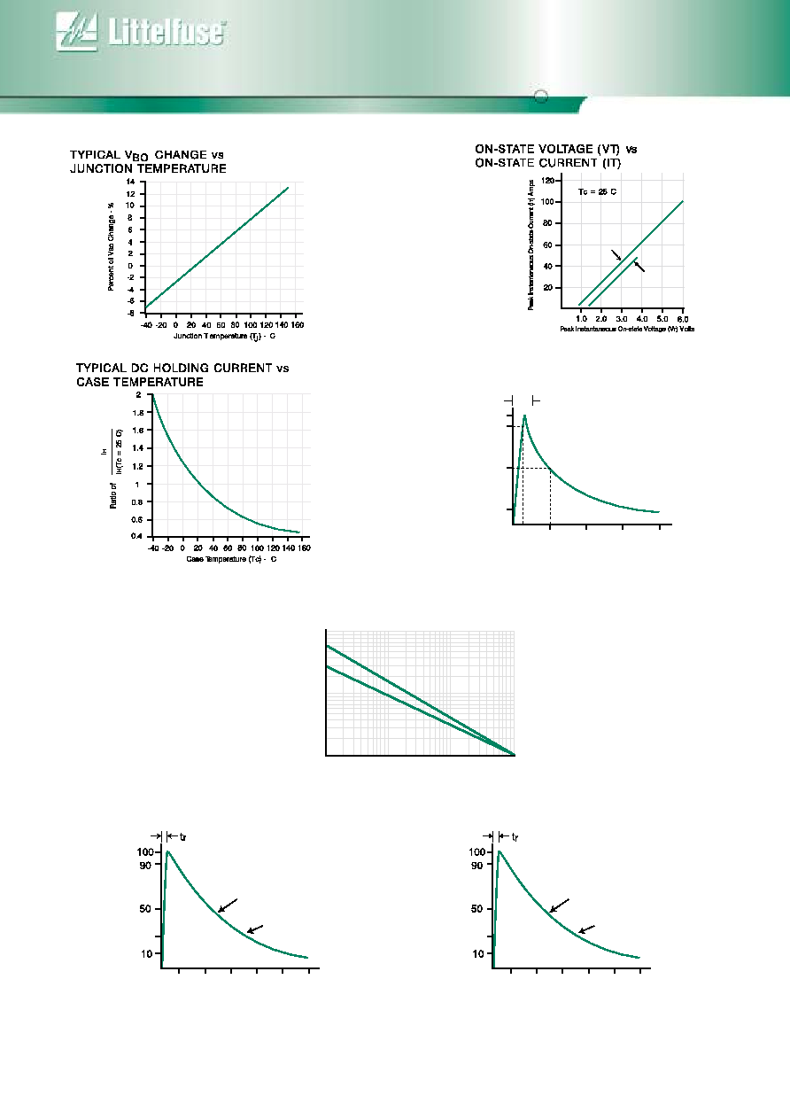
Electrical Charecteristics
The electrical characteristics of a CRXXXX device is similar
to that of a self gated Triac, but the CR is a two terminal
device with no gate. The gate function is achieved by an
internal current controlled mechanism.
Like the T.T.S. diodes, the CRXXXX has a standoff voltage
(Vrm) which should be equal to or greater than the operating
voltage of the system to be protected. At this voltage (Vrm)
the current consumption of the CRXXXX is negligible and will
not effect the protected system.
When a transient occurs, the voltage across the CRXXXX
will increase until the breakdown voltage (Vbr) is reached. At
this point the device will operate in a similar way to a T.V.S.
device and is in an avalanche mode.
The voltage of the transient will now be limited and will only
increase by a few volts as the device diverts more current.
As this transient current rises, a level of current through the
device is reached (Ibo) which causes the device to switch to
a fully conductive state such that the voltage across the
device is now only a few volts (Vt). The voltage at which the
device switches from the avalanche mode to the fully
conductive state (Vt) is known as the Breakover Voltage
(Vbo). When the device is in the Vt state, high currents can
be deverted without damage to the CRXXXX due to the low
voltage across the device, since the limiting factor in such
devices is dissipated power (V x I).
Resetting of the device to the non conducting state is
controlled by the current flowing through the device. When
the current falls below a certain value, known as the Holding
Current (Ih), the device resets automatically.
As with the avalanche T.V.S. device, if the CRXXXX is
subjected to a surge current which is beyond its maximum
rating, then the device will fail in short circuit mode, this
ensures that the equipment is ultimately protected.
Selecting A CRXXXX
1. When selecting a CRXXXX device, it is important that the
Vrm of the device is equal to or greater than the operating
voltage of the system.
2. The minimum Holding Current (Ih) must be greater than
the current the system is capable of delivering otherwise the
device will remain conducting following a transient condition.
V
BR
MIN
V
RM
V
BO
I
RM
I
BO
I
VT
H
I
T
V-I Graph
Illustrating Symbols
and Terms for
the CR Surge
Protection Device.
The CRXXXX Range Can Be Used to Protect Against Surges As Defined In The Following International Standards.
SA
SB
SC
FCC Rules Part 68/D
Metallic 10/560µs
50A
100A
100A
Longitudinal
10/160µs
100A
150A
200A
Bellcore Specification
TR-NWT-001089
10/1000µs
37A
75A
100A
2/10µs
-
-
500A
100v/µs
1KV
1KV
1KV
ITU K-17 (Formerly CCITT)
Voltage Wave Form
100/700µs
-
1.5KV
1.5KV
Current Wave Form
5/310µs
-
38A
38A
VDE 0433
Voltage Wave Form
10/700µs
-
2KV
4.0KV
Current Wave Form
5/310µs
-
50A
100A
C-NET 131-24
Voltage Wave From
0.5/700µs
1.0KV
1.0KV
4.0KV
Current Wave Form
0.8/310µs
25A
25A
100A
IEC 1000-4-5
(Discharge through 2
impendance) I
8/20µs
-
100A
250A
Voltage Wave Form
1-2/50µs
-
300V
500V
ITU K-20
Voltage Wave Form
10/700µs
1000V
10000V
4000V
(Formerly CCITT)
Current Wave Form
5/310µs
25A
25A
100A
53
w w w . l i t t e l f u s e . c o m
CRxxxx series
Specifications
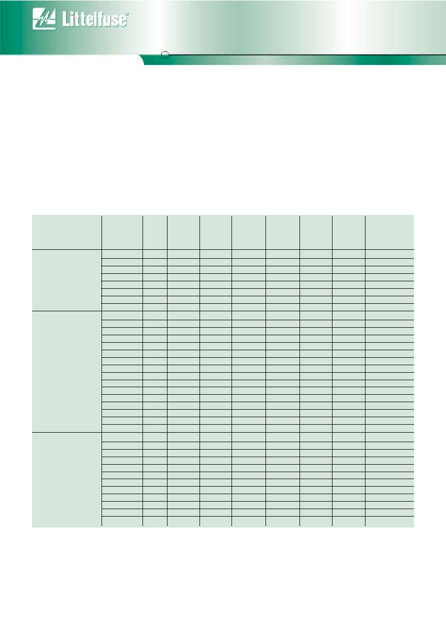
Electrical Charecteristics (Tj=25∞C)
SYMBOL
PARAMETER
SYMBOL
PARAMETER
V
RM
Stand-off Coltage
I
RM
Stand-off Current
V
BR
Breakdown Voltage
I
BO
Breakover Current
V
BO
Breakover Voltage
I
H
Holding Current
V
T
On-State Voltage
THERMAL DATA
VALUE
UNIT
T stg
Storage and Operating Junction Temperature range
-40 to +150
∞C
Tj
150
∞C
TL
Maximum Temperature For Soldering
230
∞C
(For period of 10 seconds max)
Stock
Device Reverse
Maximum
Maximum
Maximum
Minimum
Maximum
Typical
Number
Code
Stand-off
Reverse
Breakover
Breakover
Holding
On-State
Capacitance
Voltage
Leakage
Voltage
Current
Current
Voltage
@1MHz 2v bias
µA
@Ibo
mA
mA
@1A
pF
CR 0300 SA
030A
25
5
40
800
150
5
100
CR 0640 SA
064A
58
5
77
800
150
5
60
CR 0720 SA
072A
65
5
88
800
150
5
60
CR 0800 SA
080A
75
5
98
800
150
5
60
CR 1100 SA
110A
90
5
130
800
150
5
60
CR 1300 SA
130A
120
5
160
800
150
5
40
CR 1500 SA
150A
140
5
180
800
150
5
40
CR 1800 SA
180A
160
5
220
800
150
5
40
CR 2300 SA
230A
190
5
260
800
150
5
30
CR 2600 SA
260A
220
5
300
800
150
5
30
CR 3100 SA
310A
275
5
350
800
150
5
30
CR 3500 SA
350A
320
5
400
800
150
5
30
CR 0300 SB
030B
25
5
40
800
150
5
100
CR 0640 SB
064B
58
5
77
800
150
5
60
CR 0720 SB
072B
65
5
88
800
150
5
60
CR 0800 SB
080B
75
5
98
800
150
5
60
CR 1100 SB
110B
90
5
130
800
150
5
60
CR 1300 SB
130B
120
5
160
800
150
5
40
CR 1500 SB
150B
140
5
180
800
150
5
40
CR 1800 SB
180B
160
5
220
800
150
5
40
CR 2300 SB
230B
190
5
260
800
150
5
30
CR 2600 SB
260B
220
5
300
800
150
5
30
CR 3100 SB
310B
275
5
350
800
150
5
30
CR 3500 SB
350B
320
5
400
800
150
5
30
CR 0300 SC
030C
25
5
40
800
150
5
200
CR 0640 SC
064C
58
5
77
800
150
5
120
CR 0720 SC
072C
65
5
88
800
150
5
120
CR 0800 SC
080C
75
5
98
800
150
5
120
CR 1100 SC
110C
90
5
130
800
150
5
120
CR 1300 SC
130C
120
5
160
800
150
5
80
CR 1500 SC
150C
140
5
180
800
150
5
80
CR 1800 SC
180C
160
5
220
800
150
5
80
CR 2300 SC
230C
190
5
260
800
150
5
60
CR 2600 SC
260C
220
5
300
800
150
5
60
CR 3100 SC
310C
275
5
350
800
150
5
60
CR 3500 SC
350C
320
5
400
800
150
5
60
MAXIMUM RATINGS
SUFFIX
SA
Ipp 10x160µs Amps 100
Ipp 10x560µs Amps
50
I
TSM
60Hz Amps
20
DI/dt Amps/µs
500
MAXIMUM RATINGS
SUFFIX SB
Ipp 10x160µs Amps 150
Ipp 10x560µs Amps
100
I
TSM
60Hz Amps
30
DI/dt Amps/µs
500
MAXIMUM RATINGS
SUFFIX
SC
Ipp 2x10µs Amps
500
Ipp 10x160µs Amps
200
Ipp 10x560µs Amps
100
I
TSM
60Hz Amps
60
dI/dt Amps/µs
500
54
w w w . l i t t e l f u s e . c o m
CRxxxx series
∞
∞
CRXXXXSB
CRXXXXSC
CRXXXXSA
∞
10
100
50
I
PP
- P
ercentage peak current - %I
PP
2
90
td = 1000
µ
s
tr
tr = 1.25 x (t
2
- t
1
) =10
µ
s
t
2
t
1
4
1
3
t - Time
- m S e c
PULSE WAVE FORM (10/10000
µ
S)
5
300
200
1000
50
40
30
20
100
10
8
6
5
4
3
2
1
100
80
60
50
40
30
20
1
4
3
2
10
Surge Current Duration - full cycles @ 60H
Z
SINUSOIDAL
P
eak Current Surge (Non-Repetitive)
CRXXXXSB
CRXXXXSC
CRXXXXSA
On-State Current (RMS) - Amps
PEAK SURGE ON-STATE CURRENT
VS. SURGE CURRENT DURATION
10x160
µ
s PULSE WAVE FORM
Peak Value - Ipp
TEST WAVEFORM
PARAMETER
tr = 10 sec
td = 160 sec
10x160 Waveform
t - Time - Sec
Ipp - Peak Pulse Current - %Ipp
Ipp - Peak Pulse Current - %Ipp
t - Time - Sec
Half Value =
Ipp
= td
2
80
160 240
320 400
480
10x560
µ
s PULSE WAVE FORM
Peak Value - Ipp
TEST WAVEFORM
PARAMETER
tr = 10 sec
td = 560 sec
10x560 Waveform
Half Value =
Ipp
= td
2
280
0
0
560
840 1,120 1,400 1,680