 | –≠–ª–µ–∫—Ç—Ä–æ–Ω–Ω—ã–π –∫–æ–º–ø–æ–Ω–µ–Ω—Ç: LF2247-25 | –°–∫–∞—á–∞—Ç—å:  PDF PDF  ZIP ZIP |

DEVICES INCORPORATED
Video Imaging Products
1
LF2247
Image Filter with Coefficient RAM
1
2
3
4
5
6
7
8
9
10
11
08/16/2000≠LDS.2247-H
u
u
u
u
u
66 MHz Data Input and Compu-
tation Rate
u
u
u
u
u Four 11 x 10-bit Multipliers with
Individual Data and Coefficient
Inputs and a 25-bit Accumulator
u
u
u
u
u Four 32 x 11-bit Serially Loadable
Coefficient Registers
u
u
u
u
u Fractional or Integer Two's
Complement Operands
u
u
u
u
u Package Styles Available:
∑ 84-pin PLCC, J-Lead
∑ 100-pin PQFP
FEATURES
DESCRIPTION
LF2247
Image Filter with Coefficient RAM
DEVICES INCORPORATED
The LF2247 consists of an array of four
11 x 10-bit registered multipliers
followed by a summer and a 25-bit
accumulator. The LF2247 provides a
coefficient register file containing four
32 x 11-bit registers which are capable
of storing 32 different sets of filter
coefficients for the multiplier array.
All multiplier data inputs are user
accessible and can be updated every
clock cycle with either fractional or
integer two's complement data. The
pipelined architecture has fully
registered input and output ports and
an asynchronous three-state output
enable control to simplify the design
of complex systems. The pipeline
latency for all inputs is five clock
cycles.
A 25-bit accumulator path allows
cumulative word growth which may
be internally rounded to 16 bits.
Output data is updated every clock
cycle and may be held under user
control. The data inputs/outputs and
control inputs are registered on the
rising edge of CLK. The Serial Data In
signal, SDIN, is registered on the
LF2247 B
LOCK
D
IAGRAM
D1
9-0
10
11
ENB
1
D2
9-0
10
11
ENB
2
22
D3
9-0
10
11
ENB
3
D4
9-0
10
11
ENB
4
22
MS
LS
S
15-0
ACC
FSEL
OEN
CLK
TO ALL REGISTERS
(EXCEPT COEFFICIENT REGISTERS)
25
OCEN
Coefficient
Register 1
(32 x 11-bit)
Coefficient
Register 2
(32 x 11-bit)
Coefficient
Register 3
(32 x 11-bit)
Coefficient
Register 4
(32 x 11-bit)
A
4-0
SEN
SDIN
SCLK
SCLK
5
ENBA
16
COEFFICIENT REGISTER FILE
SEN
SCLK
SEN
SCLK
SEN
DEVICES INCORPORATED
LF2247
Image Filter with Coefficient RAM
-2
Video Imaging Products
08/16/2000≠LDS.2247-H
rising edge of SCLK. The LF2247
operates at a clock rate of 66 MHz
over the full temperature and supply
voltage ranges.
The LF2247 is applicable for perform-
ing pixel interpolation in image
manipulation and filtering applica-
tions. The LF2247 can perform a
bilinear interpolation of an image (4-
pixel kernels) at real-time video rates
when used with an image resampling
sequencer. Larger kernels or more
complex functions can be realized by
utilizing multiple devices.
Unrestricted access to all data ports
and an addressable coefficient register
file provides the LF2247 with consid-
erable flexibility in applications such
as digital filters, adaptive FIR filters,
mixers, and other similar systems
requiring high-speed processing.
SIGNAL DEFINITIONS
Power
V
CC
and GND
+5 V power supply. All pins must be
connected.
Clocks
CLK -- Master Clock
The rising edge of CLK strobes all
enabled registers except for the
coefficient registers.
SCLK -- Serial Clock
The rising edge of SCLK shifts data
into and through the coefficient
register file when it is enabled for
serial data shifting.
Inputs
D1
9-0
≠ D4
9-0
-- Data Input
D1≠D4 are the 10-bit registered data
input ports. Data is latched on the
rising edge of CLK.
A
4-0
-- Row Address
A
4-0
determines which row of data in
the coefficient register file is used to
feed data to the multiplier array. A
4-0
is latched on the rising edge of CLK.
When a new row address is loaded
into the row address register, data
from the register file will be latched
into the multiplier input registers on
the next rising edge of CLK.
SDIN -- Serial Data Input
SDIN is used to serially load data into
the coefficient registers. Data present
on SDIN is shifted into the coefficient
register file on the rising edge of SCLK
when SEN is LOW. The 11-bit coeffi-
cients are loaded into the coefficient
register file in 16-bit words as shown
in Figure 2. The five most significant
bits of the first 16-bit word determine
which row the data is written to in the
coefficient registers. Note that the five
most significant bits of the remaining
three 16-bit words are ignored. After
all four 16-bit words are shifted into
the register file, the lower eleven bits
of each word (the coefficient data) are
stored into the coefficient registers.
Outputs
S
15-0
-- Data Output
S
15-0
is the 16-bit registered data
output port.
Controls
ENB
1
≠ENB
4
-- Data Input Enables
The ENB
N
(
N
= 1, 2, 3, or 4) inputs
allow the DN registers to be updated
on each clock cycle. When ENB
N
is
LOW, data on DN
9-0
is latched into
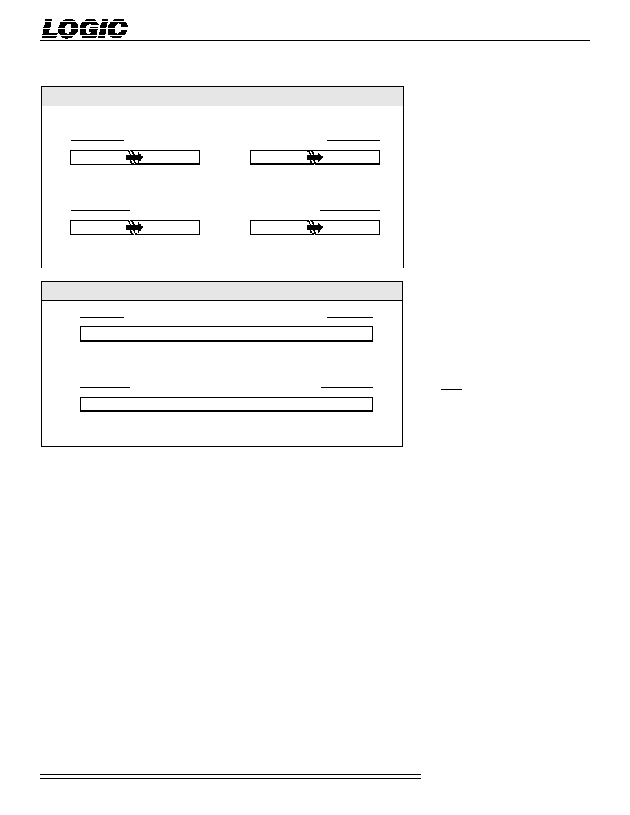
F
IGURE
1
B
.
O
UTPUT
F
ORMATS
15 14 13
10
9
8
12 11
7
6
5
4
3
2
1
0
≠2
6
(Sign)
2
5
2
4
2
1
2
0
2
≠1
2
3
2
2
2
≠2
2
≠3
2
≠4
2
≠5
2
≠6
2
≠7
2
≠8
2
≠9
15 14 13
10
9
8
12 11
7
6
5
4
3
2
1
0
≠2
15
(Sign)
2
14
2
13
2
10
2
9
2
8
2
12
2
11
2
7
2
6
2
5
2
4
2
3
2
2
2
1
2
0
Fractional Two's Complement (FSEL = 0)
Integer Two's Complement (FSEL = 1)
F
IGURE
1
A
.
I
NPUT
F
ORMATS
9
8
7
2
1
0
≠2
0
(Sign)
2
≠1
2
≠2
2
≠7
2
≠8
2
≠9
10
9
8
2
1
0
≠2
1
(Sign)
2
0
2
≠1
2
≠7
2
≠8
2
≠9
9
8
7
2
1
0
≠2
9
(Sign)
2
8
2
7
2
2
2
1
2
0
10
9
8
2
1
0
≠2
10
(Sign)
2
9
2
8
2
2
2
1
2
0
Fractional Two's Complement (FSEL = 0)
Integer Two's Complement (FSEL = 1)
Data
Coefficient

DEVICES INCORPORATED
Video Imaging Products
3
LF2247
Image Filter with Coefficient RAM
1
2
3
4
5
6
7
8
9
10
11
08/16/2000≠LDS.2247-H
the DN register on the rising edge of
CLK. When ENB
N
is HIGH, data on
DN
9-0
is not latched into the DN
register and the register contents will
not be changed.
ENBA -- Row Address Input Enable
The ENBA input allows the row
address register to be updated on each
clock cycle. When ENBA is LOW,
data on A
4-0
is latched into the row
address register on the rising edge of
CLK. When ENBA is HIGH, data on
A
4-0
is not latched into the row
address register and the register
contents will not be changed.
OEN -- Output Enable
When OEN is LOW, S
15-0
is enabled
for output. When OEN is HIGH, S
15-0
is placed in a high-impedance state.
OCEN -- Clock Enable
When OCEN is LOW, data in the pre-
mux register (accumulator output) is
loaded into the output register on the
next rising edge of CLK. When OCEN
is HIGH, data in the pre-mux register
is held preventing the output
register's contents from changing (if
FSEL does not change). Accumulation
continues internally as long as ACC is
HIGH, despite the state of OCEN.
FSEL -- Format Select
When FSEL is LOW, the data input
during the current clock cycle is
assumed to be in fractional two's
complement format, and the upper 16
bits of the accumulator are presented
at the output. Rounding of the
accumulator result to 16 bits is per-
formed if the accumulator control
input ACC is LOW. When FSEL is
HIGH, the data input is assumed to be
in integer two's complement format,
and the lower 16 bits of the accumula-
tor are presented at the output. No
rounding is performed when FSEL is
HIGH.
ACC -- Accumulator Control
The ACC input determines whether
internal accumulation is performed on
the data input during the current
clock cycle. If ACC is LOW, no
accumulation is performed, the prior
accumulated sum is cleared, and the
current sum of products is output. If
FSEL is also LOW, one-half LSB
rounding to 16 bits is performed on
the result. When ACC is HIGH, the
emerging product is added to the sum
of the previous products, without
additional rounding.
SEN -- Serial Input Enable
The SEN input enables the shifting of
serial data through the registers in the
coefficient register file. When SEN is
LOW, serial data on SDIN is shifted
into the coefficient register file on the
rising edge of SCLK. SEN must
remain LOW until all four coefficients
have been clocked in. SEN does not
need to be pulsed between consecu-
tive data sets. It can remain LOW
while the entire register file is loaded
by a constant bit stream. When SEN is
HIGH, data can not be shifted into the
register file and the register file's
contents will not be changed. When
enabling the coefficient register file for
serial data input, the LF2247 requires
a HIGH to LOW transition of SEN in
order to function properly. Therefore,
SEN needs to be set HIGH immedi-
ately after power up to ensure proper
operation of the serial input circuitry.
F
IGURE
2.
S
ERIAL
D
ATA
F
ORMAT
2 3
1
5 6
4
8 9
7
11 12
10
13
15 16
14
18 19
17
21 22
20
24 25
23
27 28
26
29
31 32
30
34 35
33
37 38
36
40 41
39
43 44
42
45
47 48
46
50 51
49
53 54
52
56 57
55
59 60
58
61
63 64
62
0 0
0
0 1
1
1 1
1
1 0
1
1
0 0
1
X X
X
X 0
X
0 1
0
0 0
0
1
0 0
1
X X
X
X 0
X
1 1
0
1 0
0
0
0 0
1
X X
X
X 1
X
1 1
1
1 0
1
0
0 0
1
FIRST 16-BIT WORD
SECOND 16-BIT WORD
THIRD 16-BIT WORD
FOURTH 16-BIT WORD
ROW
ADDRESS
DATA FOR
COEFFICIENT REGISTER 4
DON'T
CARES
DATA FOR
COEFFICIENT REGISTER 3
DON'T
CARES
DATA FOR
COEFFICIENT REGISTER 2
DON'T
CARES
DATA FOR
COEFFICIENT REGISTER 1
SHOWN IS SERIAL DATA STREAM TO LOAD ROW ADDRESS 2 WITH:
COEFFICIENT REGISTER 1 = 7E4
COEFFICIENT REGISTER 2 = 1A4
COEFFICIENT REGISTER 3 = 08C
COEFFICIENT REGISTER 4 = 7EC

DEVICES INCORPORATED
LF2247
Image Filter with Coefficient RAM
-4
Video Imaging Products
08/16/2000≠LDS.2247-H
Storage temperature ........................................................................................................... ≠65∞C to +150∞C
Operating ambient temperature ........................................................................................... ≠55∞C to +125∞C
V
CC
supply voltage with respect to ground ............................................................................ ≠0.5 V to +7.0 V
Input signal with respect to ground ............................................................................... ≠0.5 V to V
CC
+ 0.5 V
Signal applied to high impedance output ...................................................................... ≠0.5 V to V
CC
+ 0.5 V
Output current into low outputs ............................................................................................................. 25 mA
Latchup current ............................................................................................................................... > 400 mA
M
AXIMUM
R
ATINGS
Above which useful life may be impaired (Notes 1, 2, 3, 8)
Symbol
Parameter
Test Condition
Min
Typ
Max
Unit
V
OH
Output High Voltage
V
CC
= Min., I
OH
= ≠2.0 mA
2.4
V
V
OL
Output Low Voltage
V
CC
= Min., I
OL
= 4.0 mA
0.4
V
V
IH
Input High Voltage
2.0
V
CC
V
V
IL
Input Low Voltage
(Note 3)
0.0
0.8
V
I
IX
Input Current
Ground
V
IN
V
CC
(Note 12)
±
10
µA
I
OZ
Output Leakage Current
Ground
V
OUT
V
CC
(Note 12)
±
40
µA
I
CC1
V
CC
Current, Dynamic
(Notes 5, 6)
100
mA
I
CC2
V
CC
Current, Quiescent
(Note 7)
6.0
mA
C
IN
Input Capacitance
T
A
= 25∞C, f = 1 MHz
10
pF
C
OUT
Output Capacitance
T
A
= 25∞C, f = 1 MHz
10
pF
E
LECTRICAL
C
HARACTERISTICS
Over Operating Conditions (Note 4)
O
PERATING
C
ONDITIONS
To meet specified electrical and switching characteristics
Mode
Temperature Range (Ambient)
Supply
Voltage
Active Operation, Commercial
0∞C to +70∞C
4.75 V
V
CC
5.25 V
Active Operation, Military
≠55∞C to +125∞C
4.50 V
V
CC
5.50 V

DEVICES INCORPORATED
Video Imaging Products
5
LF2247
Image Filter with Coefficient RAM
1
2
3
4
5
6
7
8
9
10
11
08/16/2000≠LDS.2247-H
1234567890123456
1234567890123456
1234567890123456
1234567890123456
1234567890123456
1234567890123456
1234567890123456
1234567890123456
1234567890123456
1234567890123456
1234567890123456
1234567890123456
1234567890123456
1234567890123456
1234567890123456
1234567890123456
1234567890123456
1234567890123456
1234567890123456
1234567890123456
1234567890123456
1234567890123456
1234567890123456
1234567890123456
1234567890123456
1234567890123456
1234567890123456
1234567890123456
1234567890123456
1234567890123456
1234567890123456
1234567890123456
1234567890123456789012345678901
1234567890123456789012345678901
1234567890123456789012345678901
1234567890123456789012345678901
1234567890123456789012345678901
1234567890123456789012345678901
1234567890123456789012345678901
1234567890123456789012345678901
1234567890123456789012345678901
1234567890123456789012345678901
1234567890123456789012345678901
1234567890123456789012345678901
1234567890123456789012345678901
1234567890123456789012345678901
1234567890123456789012345678901
1234567890123456789012345678901
1234567890123456789012345678901
1234567890123456789012345678901
1234567890123456789012345678901
1234567890123456789012345678901
1234567890123456789012345678901
1234567890123456789012345678901
1234567890123456789012345678901
1234567890123456789012345678901
1234567890123456789012345678901
1234567890123456789012345678901
1234567890123456789012345678901
1234567890123456789012345678901
1234567890123456789012345678901
1234567890123456789012345678901
1234567890123456789012345678901
1234567890123456789012345678901
SWITCHING CHARACTERISTICS
LF2247≠
33*
25
15
Symbol
Parameter
Min
Max
Min
Max
Min
Max
t
CYC
Cycle Time
33
25
15
t
PWL
Clock Pulse Width Low
15
10
7
t
PWH
Clock Pulse Width High
10
10
7
t
S
Input Setup Time
10
8
5
t
H
Input Hold Time
0
0
0
t
D
Output Delay
15
13
11
t
DIS
Three-State Output Disable Delay
(Note 11)
15
15
15
t
ENA
Three-State Output Enable Delay
(Note 11)
15
15
15
C
OMMERCIAL
O
PERATING
R
ANGE
(0∞C to +70∞C)
Notes 9, 10 (ns)
LF2247≠
33*
25*
Symbol
Parameter
Min
Max
Min
Max
t
CYC
Cycle Time
33
25
t
PWL
Clock Pulse Width Low
15
10
t
PWH
Clock Pulse Width High
10
10
t
S
Input Setup Time
10
8
t
H
Input Hold Time
0
0
t
D
Output Delay
15
13
t
DIS
Three-State Output Disable Delay
(Note 11)
15
15
t
ENA
Three-State Output Enable Delay
(Note 11)
15
15
M
ILITARY
O
PERATING
R
ANGE
(≠55∞C to +125∞C)
Notes 9, 10 (ns)
123456789012345678901234
123456789012345678901234
123456789012345678901234
*D
ISCONTINUED
S
PEED
G
RADE
S
WITCHING
W
AVEFORMS
:
D
ATA
I/O
CLK
D1
9-0
≠ D4
9-0
CONTROLS
t
PWH
t
PWL
t
CYC
A
4-0
(Except OEN)
OEN
S
15-0
1
2
3
4
5
6
t
H
t
S
D
N
D
N+1
A
N+1
A
N+2
t
D
t
DIS
HIGH IMPEDANCE
t
ENA
S
N
S
N≠1
S
N+1