 | –≠–ª–µ–∫—Ç—Ä–æ–Ω–Ω—ã–π –∫–æ–º–ø–æ–Ω–µ–Ω—Ç: LF3347 | –°–∫–∞—á–∞—Ç—å:  PDF PDF  ZIP ZIP |
DEVICES INCORPORATED
Video Imaging Products
LF3347
High-Speed Image Filter with Coefficient RAM
08/16/2000≠LDS.3347-G
1
u
u
u
u
u 83 MHz Data Input and Compu-
tation Rate
u
u
u
u
u Four 12 x 12-bit Multipliers with
Individual Data and Coefficient
Inputs
u
u
u
u
u Four 256 x 12-bit Coefficient Banks
u
u
u
u
u 32-bit Accumulator
u
u
u
u
u Selectable 16-bit Data Output with
User-Defined Rounding and Limiting
u
u
u
u
u Two's Complement Operands
u
u
u
u
u 3.3 Volt Power Supply
u
u
u
u
u 5 Volt Tolerant I/O
u
u
u
u
u 120-pin PQFP
FEATURES
DESCRIPTION
LF3347
High-Speed Image Filter with Coefficient RAM
DEVICES INCORPORATED
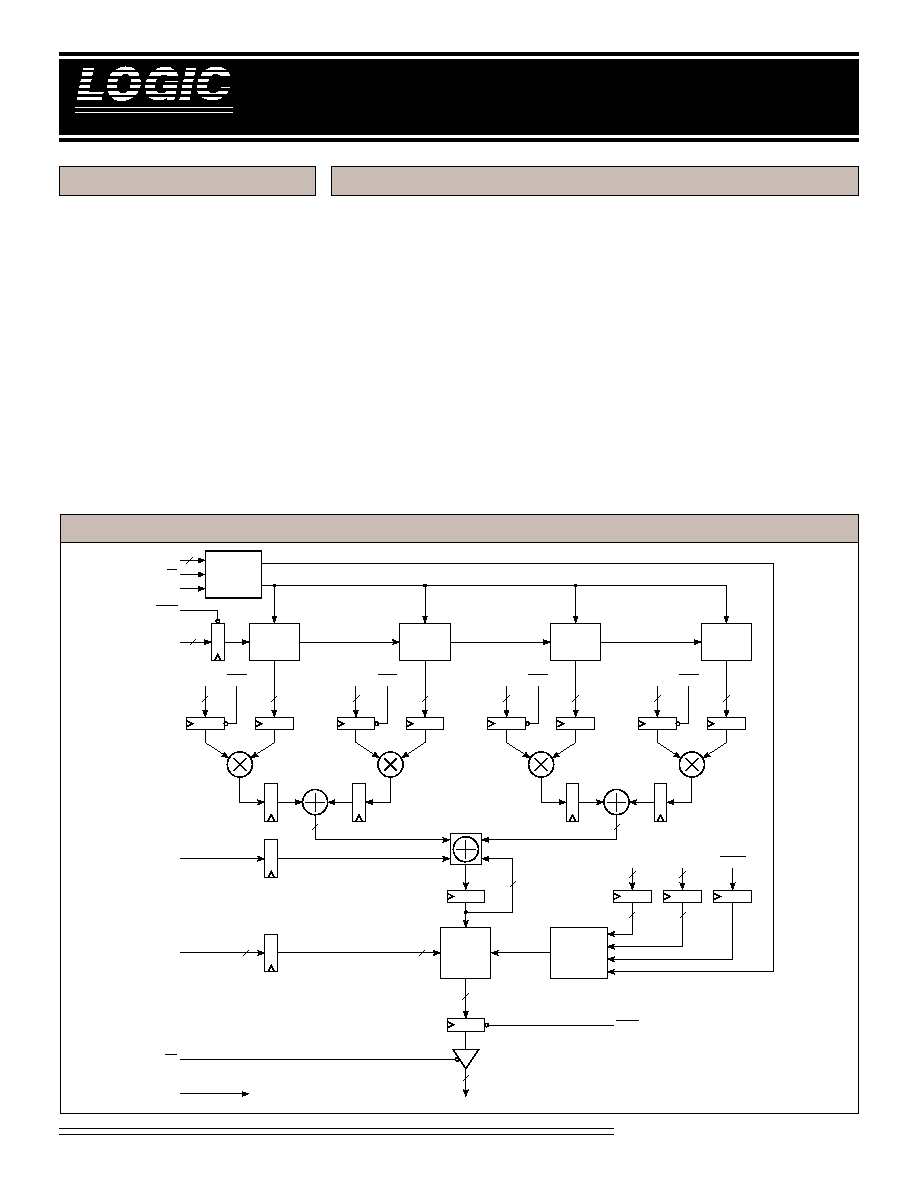
The LF3347 consists of an array of
four 12 x 12-bit registered multipliers
followed by two summers and a
32-bit accumulator. The LF3347
provides four 256 x 12-bit coefficient
banks which are capable of storing
256 different sets of filter coefficients
for the multiplier array. All multi-
plier data inputs are user accessible
and can be updated every clock cycle
with two's complement data. The
pipelined architecture has fully
registered input and output ports and
an asynchronous three-state output
enable control to simplify the design
of complex systems.
A 32-bit accumulator allows cumula-
tive word growth which may be
internally rounded to 16-bits. Output
data is updated every clock cycle and
may be held under user control. The
data inputs/outputs and control
inputs are registered on the rising
edge of CLK. The Control/Coeffi-
cient Data Input, CC
11-0
, is registered
on the rising edge of CCCLK.
The LF3347 is ideal for performing
pixel interpolation in image manipu-
lation and filtering applications. The
LF3347 can perform a bilinear inter-
polation of an image (4-pixel kernels)
at real-time video rates when used
LF3347 B
LOCK
D
IAGRAM
D1
11-0
12
12
ENB
1
D2
11-0
12
12
ENB
2
25
D3
11-0
12
12
ENB
3
D4
11-0
12
12
ENB
4
25
S
15-0
ACC
OE
CLK
TO ALL REGISTERS
Coefficient
Bank 1
(256 x 12-bit)
Coefficient
Bank 2
(256 x 12-bit)
Coefficient
Bank 3
(256 x 12-bit)
Coefficient
Bank 4
(256 x 12-bit)
A
7-0
8
ENBA
16
16
CC
11-0
12
LD
Rounding
Selecting
Limiting
Circuit
Rounding/
Limiting
Registers
CCCLK
32
OCEN
4
6
6
NOTE: NUMBERS IN REGISTERS INDICATE
NUMBER OF PIPELINE DELAYS
3
2
2
2
2
SHIFT
4-0
LMTEN
SELLMT
3-0
SELRND
3-0
5
5
4
4
5
4
4
LF
INTERFACE
DEVICES INCORPORATED
LF3347
High-Speed Image Filter with Coefficient RAM
2
Video Imaging Products
08/16/2000≠LDS.3347-G
with an image resampling se-
quencer. Larger kernels or more
complex functions can be realized
by utilizing multiple devices.
Unrestricted access to all data
ports and addressable coefficient
banks provides the LF3347 with
considerable flexibility in applica-
tions such as digital filters, adap-
tive FIR filters, mixers, and other
similar systems requiring high-
speed processing.
SIGNAL DEFINITIONS
Power
V
CC
and GND
+3.3 V power supply. All pins must
be connected.
Clocks
CLK -- Master Clock
The rising edge of CLK strobes all
enabled registers.
CCCLK -- Coefficient/Control Clock
When LD is LOW, the rising edge of
CCCLK latches data on CC
11-0
into the
device.
Inputs
D1
11-0
≠ D4
11-0
-- Data Input
D1≠D4 are the 12-bit registered data
input ports. Data is latched on the
rising edge of CLK.
A
7-0
-- Row Address
A
7-0
determines which row in the
coefficient banks feed data to the
multipliers. A
7-0
is latched on the
rising edge of CLK. When a new
row address is loaded into the row
address register, data from the
coefficient banks will be latched into
the multiplier input registers on the
next rising edge of CLK.
CC
11-0
-- Control/Coefficient Data Input
CC
11-0
is used to load data into the
coefficient banks and control regis-
ters. Data present on CC
11-0
is
latched on the rising edge of CCCLK
when LD is LOW.
Outputs
S
15-0
-- Data Output
S
15-0
is the 16-bit registered data
output port.
Controls
ENB
1
≠ENB
4
-- Data Input Enables
The ENB
N
(
N
= 1, 2, 3, or 4) inputs
allow the D
N
registers to be updated
on each clock cycle. When ENB
N
is
LOW, data on D
N11-0
is latched into
the D
N
register on the rising edge of
CLK. When ENB
N
is HIGH, data on
D
N11-0
is not latched into the D
N
register and the register contents
will not be changed.
ENBA -- Row Address Input Enable
The ENBA input allows the row
address register to be updated on
each clock cycle. When ENBA is
LOW, data on A
7-0
is latched into
the row address register on the rising
edge of CLK. When ENBA is HIGH,
data on A
7-0
is not latched into the
row address register and the register
contents will not be changed.
OE -- Output Enable
When OE is LOW, S
15-0
is enabled for
output. When OE is HIGH, S
15-0
is
placed in a high-impedance state.
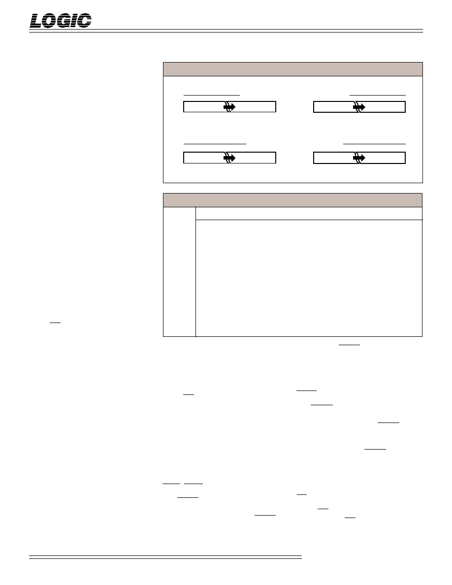
F
IGURE
1.
I
NPUT
F
ORMATS
T
ABLE
1.
O
UTPUT
F
ORMATS
SHIFT
4-0
S
15
S
14
S
13
∑ ∑ ∑
S
8
S
7
∑ ∑ ∑
S
2
S
1
S
0
00000
F
15
F
14
F
13
∑ ∑ ∑
F
8
F
7
∑ ∑ ∑
F
2
F
1
F
0
00001
F
16
F
15
F
14
∑ ∑ ∑
F
9
F
8
∑ ∑ ∑
F
3
F
2
F
1
00010
F
17
F
16
F
15
∑ ∑ ∑
F
10
F
9
∑ ∑ ∑
F
4
F
3
F
2
∑
∑
∑
∑
∑
∑
∑
∑
∑
∑
∑
∑
∑
∑
∑
∑
∑
∑
∑
∑
∑
∑
∑
∑
∑
∑
∑
01110
F
29
F
28
F
27
∑ ∑ ∑
F
22
F
21
∑ ∑ ∑
F
16
F
15
F
14
01111
F
30
F
29
F
28
∑ ∑ ∑
F
23
F
22
∑ ∑ ∑
F
17
F
16
F
15
10000
F
31
F
30
F
29
∑ ∑ ∑
F
24
F
23
∑ ∑ ∑
F
18
F
17
F
16
11 10 9
2
1
0
≠2
0
(Sign)
2
≠1
2
≠2
2
≠9
2
≠10
2
≠11
11 10 9
2
1
0
≠2
0
(Sign)
2
≠1
2
≠2
2
≠9
2
≠10
2
≠11
11 10 9
2
1
0
≠2
11
(Sign)
2
10
2
9
2
2
2
1
2
0
11 10 9
2
1
0
≠2
11
(Sign)
2
10
2
9
2
2
2
1
2
0
Fractional Two's Complement
Integer Two's Complement
Data
Coefficient
DEVICES INCORPORATED
Video Imaging Products
LF3347
High-Speed Image Filter with Coefficient RAM
08/16/2000≠LDS.3347-G
3
OCEN -- Output Clock Enable
When OCEN is LOW, the output
register is enabled for data loading.
When OCEN is HIGH, output register
loading is disabled and the register's
contents will not change.
ACC -- Accumulator Control
The ACC input determines whether
internal accumulation is performed. If
ACC is LOW, no accumulation is
performed, the prior accumulated sum
is cleared, and the current sum of
products is output. When ACC is
HIGH, the emerging product is added
to the sum of the previous products.
LD -- Load Control
LD enables the loading of data into the
coefficient banks and control registers
(control registers are the round and limit
registers). When LD is LOW, data on
CC
11-0
is latched into the device on the
rising edge of CCCLK. When LD is
HIGH, data cannot be loaded into the
coefficient banks and control registers.
When enabling the input circuitry for
data loading, the LF3347 requires a
HIGH to LOW transition of LD in order
to function properly. Therefore, LD
needs to be set HIGH immediately after
power up to ensure proper operation of
the input circuitry.
It takes five CCCLK clock cycles to load
one coefficient set into the four coefficient
banks or to load one control register.
When the input circuitry is enabled (LD
goes LOW), the first value loaded into the
device on CC
11-0
is an address which
determines what will be loaded (see
Table 2). The next four values loaded on
CC
11-0
is the data to be loaded into the
coefficient banks or control register (see
Tables 3-5). After the last data value is
loaded, another coefficient bank address
or control register may be loaded by
feeding another address into CC
11-0
.
When all desired coefficient banks and
control registers are loaded, the input
circuitry must be disabled by setting LD HIGH.
SELRND
3-0
-- Round Select
SELRND
3-0
allows the user to select
which rounding register will be used
in the rounding circuit to round/offset
the data.
SHIFT
4-0
-- Shift
SHIFT
4-0
determines which 16-bits of
the 32-bits from the accumulator are
passed to the output (see Table 1).
SELLMT
3-0
-- Limit Select
SELLMT
3-0
allows the user to control
which limiting register will be used in
the limiting circuit to set the upper
and lower limits on the data.
LMTEN -- Limit Enable
When LMTEN is LOW, limiting is
enabled and the selected limit register
is used to determine the valid range of
output values for the overall filter.
When HIGH, limiting is disabled.
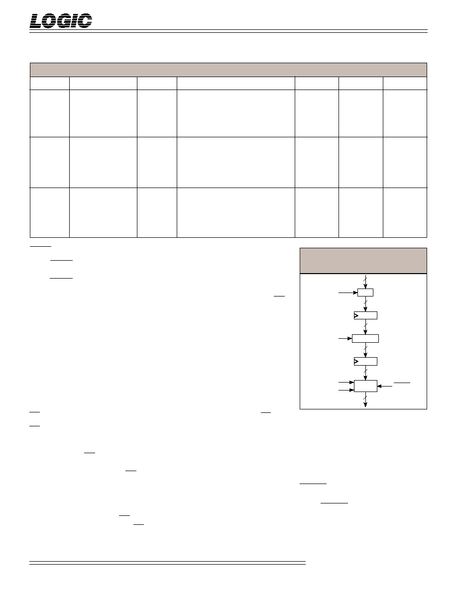
F
IGURE
2. R
OUNDING
, S
ELECTING
,
L
IMITING
C
IRCUITRY
RND
SELECT
LIMIT
32
16
LMTEN
32
SHIFT
4-0
ULMT
15-0
LLMT
15-0
RND
31-0
16
16
32
Register
Load Address
Bits
Register Description
A
7-0
SELRND
3-0
SELLMT
3-0
CS0
000H
11-0
Coefficient Set 0
00H
CS1
001H
11-0
Coefficient Set 1
01H
∑
∑
∑
∑
∑
∑
∑
∑
∑
∑
∑
∑
∑
∑
∑
CS255
0FFH
11-0
Coefficient Set 255
FFH
RND0
800H
31-0
Rounding Register 0
0 0 0 0
RND1
801H
31-0
Rounding Register 1
0 0 0 1
∑
∑
∑
∑
∑
∑
∑
∑
∑
∑
∑
∑
∑
∑
∑
RND15
80FH
31-0
Rounding Register 15
1 1 1 1
LMT0
C00H
31-16/15-0
Upper / Lower Limit Register 0
0 0 0 0
LMT1
C01H
31-16/15-0
Upper / Lower Limit Register 0
0 0 0 1
∑
∑
∑
∑
∑
∑
∑
∑
∑
∑
∑
∑
∑
∑
∑
LMT15
C0FH
31-16/15-0
Upper / Lower Limit Register 15
1 1 1 1
T
ABLE
2.
R
EGISTER
F
ORMATS
DEVICES INCORPORATED
LF3347
High-Speed Image Filter with Coefficient RAM
4
Video Imaging Products
08/16/2000≠LDS.3347-G
FUNCTIONAL DESCRIPTION
Coefficient Banks
The LF3347 has four coefficient banks
which feed coefficient values to the
multipliers. Each bank can store 256
12-bit coefficients. In the example
shown in Table 3, address 10 in coeffi-
cient banks 1 through 4 is loaded with
the following values: ABCH, 789H,
456H, 123H. The coefficient banks are
not written to until all four coefficients
have been loaded into the device.
A
7-0
determines which coefficient set is
sent to the multipliers. A value of 0 on
A
7-0
selects set 0. A value of 1 selects
set 1 and so on.
Rounding/Offset
The accumulator output may be rounded
before being sent to the output select
section. Rounding is user-selectable and
is accomplished by adding the contents of
a round register to the accumulator
output (see Figure 2). There are sixteen
32-bit round registers. In the example in
Table 4, round register 10 is loaded with
76543210H. A round register is not
written to until all four data values have
been loaded into the device.
SELRND
3-0
determines which round
register is used for rounding. A value of 0
on SELRND
3-0
selects round register 0. A
value of 1 selects round register 1 and so
on. If rounding is not desired, a round
register should be loaded with 0 and
selected as the register for rounding.
Output Select
The filter output word width is 32-bits.
However, only 16-bits may be sent to the
device output. SHIFT4-0 determines
which 16 bits are passed to the device
output (See Table 1).
Output Limiting
An output limiting function is provided
for the output of the filter. When limiting is
enabled (LMTEN LOW), the limit register
selected with SELLMT
3-0
determines the
valid range of output values for the overall
filter. There are sixteen 32-bit limit
registers. Each limit register contains both
an upper and lower limit value. The
lower limit is stored in bits 15-0 and the
upper limit is stored in bits 31-16. If the
value fed to the limiting circuitry is less
than the lower limit, the lower limit is
passed to the device output. If the value
fed to the limiting circuitry is greater than
the upper limit, the upper limit is passed
to the device output. When loading limit
values into the device, the upper limit must
T
ABLE
3.
C
OEFFICIENT
B
ANK
L
OADING
F
ORMAT
CC
11
CC
10
CC
9
CC
8
CC
7
CC
6
CC
5
CC
4
CC
3
CC
2
CC
1
CC
0
1st Word
0
0
0
0
0
0
0
0
1
0
1
0
Address
2nd Word
1
0
1
0
1
0
1
1
1
1
0
0
Bank 1
3rd Word
0
1
1
1
1
0
0
0
1
0
0
1
Bank 2
4th Word
0
1
0
0
0
1
0
1
0
1
1
0
Bank 3
5th Word
0
0
0
1
0
0
1
0
0
0
1
1
Bank 4
T
ABLE
4.
R
OUND
R
EGISTER
L
OADING
F
ORMAT
CC
11
CC
10
CC
9
CC
8
CC
7
CC
6
CC
5
CC
4
CC
3
CC
2
CC
1
CC
0
1st Word
1
0
0
0
0
0
0
0
1
0
1
0
Address
2nd Word
R
R
R
R
0
0
0
1
0
0
0
*0
3rd Word
R
R
R
R
0
0
1
1
0
0
1
0
4th Word
R
R
R
R
0
1
0
1
0
1
0
0
5th Word
R
R
R
R
**0
1
1
1
0
1
1
0
T
ABLE
5.
L
IMIT
R
EGISTER
L
OADING
F
ORMAT
CC
11
CC
10
CC
9
CC
8
CC
7
CC
6
CC
5
CC
4
CC
3
CC
2
CC
1
CC
0
1st Word
1
1
0
0
0
0
0
0
1
1
1
1
Address
2nd Word
R
R
R
R
0
0
1
0
0
0
1
1
3rd Word
R
R
R
R
*0
0
0
0
0
0
0
1
4th Word
R
R
R
R
1
1
1
0
1
1
0
1
5th Word
R
R
R
R
**0
1
1
1
1
1
1
1
R = Reserved. Must be set to "0".
* This bit represents the MSB of the Lower Limit Register.
** This bit represents the MSB of Upper Limit Register.
R = Reserved. Must be set to "0".
* This bit represents the LSB of the Round Register.
** This bit represents the MSB of the Round Register.
be greater than the lower limit. In the
example shown in Table 4, limit register
15 is loaded with a lower limit of 0123H
and an upper limit of 7FEDH. A limit
register is not written to until all four data
values have been loaded into the device.
SELLMT
3-0
determines which limit
register is used for limiting. A value of 0
on SELLMT
3-0
selects limit register 0. A
value of 1 selects limit register 1 and so on.

DEVICES INCORPORATED
Video Imaging Products
LF3347
High-Speed Image Filter with Coefficient RAM
08/16/2000≠LDS.3347-G
5
Storage temperature ........................................................................................................... ≠65∞C to +150∞C
Operating ambient temperature ........................................................................................... ≠55∞C to +125∞C
V
CC
supply voltage with respect to ground ............................................................................ ≠0.5 V to +4.5 V
Input signal with respect to ground .......................................................................................... ≠0.5 V to 5.5 V
Signal applied to high impedance output ................................................................................. ≠0.5 V to 5.5 V
Output current into low outputs ............................................................................................................. 25 mA
Latchup current ............................................................................................................................... > 400 mA
ESD Classification (MIL-STD-883E METHOD 3015.7) ...................................................................... Class 3
M
AXIMUM
R
ATINGS
Above which useful life may be impaired (Notes 1, 2, 3, 8)
Symbol
Parameter
Test Condition
Min
Typ
Max
Unit
V
OH
Output High Voltage
V
CC
= Min., I
OH
= ≠4 mA
2.4
V
V
OL
Output Low Voltage
V
CC
= Min., I
OL
= 8.0 mA
0.4
V
V
IH
Input High Voltage
2.0
V
CC
V
V
IL
Input Low Voltage
(Note 3)
0.0
0.8
V
I
IX
Input Current
Ground
V
IN
V
CC
(Note 12)
±
10
µA
I
OZ
Output Leakage Current
Ground
V
OUT
V
CC
(Note 12)
±
10
µA
I
CC1
V
CC
Current, Dynamic
(Notes 5, 6)
150
mA
I
CC2
V
CC
Current, Quiescent
(Note 7)
2
mA
C
IN
Input Capacitance
T
A
= 25∞C, f = 1 MHz
10
pF
C
OUT
Output Capacitance
T
A
= 25∞C, f = 1 MHz
10
pF
E
LECTRICAL
C
HARACTERISTICS
Over Operating Conditions (Note 4)
O
PERATING
C
ONDITIONS
To meet specified electrical and switching characteristics
Mode
Temperature Range (Ambient)
Supply
Voltage
Active Operation, Commercial
0∞C to +70∞C
3.00 V
V
CC
3.60 V
Active Operation, Military
≠55∞C to +125∞C
3.00 V
V
CC
3.60 V