DEVICES INCORPORATED
Video Imaging Products
1
LF48410
1024 x 24-bit Video Histogrammer
08/08/2000≠LDS.48410-L
u
u
u
u
u
40 MHz Data Input and Compu-
tation Rate
u
u
u
u
u 1024 x 24-bit Memory Array
u
u
u
u
u Histograms of Images up to 4K x
4K with 10-bit Pixel Resolution
u
u
u
u
u Memory Array Flash Clear
u
u
u
u
u User-Programmable Modes:
Histogram, Histogram Accumulate,
Look Up Table, Bin Accumulate,
Delay Memory, Delay and Subtract,
Single Port RAM
u
u
u
u
u Replaces Harris HSP48410
u
u
u
u
u 84-pin PLCC, J-Lead
FEATURES
DESCRIPTION
LF48410
1024 x 24-bit Video Histogrammer
DEVICES INCORPORATED
The LF48410 is capable of generating
histograms and Cumulative Distribu-
tion Functions of video images. It
may also be used as a look up table, a
bin accumulator, a delay memory
(delay and subtract also possible), or a
single port RAM. The on-chip 1024 x
24-bit memory array facilitates
histograms of images up to 4K x 4K
pixels with a 10-bit pixel resolution.
Once the histogram of a video image
is stored in the memory array, the
Cumulative Distribution Function can
be calculated by putting the device in
Histogram Accumulate Mode.
Transformation functions can be
performed on pixel values when the
device is in Look Up Table Mode. If
the Cumulative Distribution Function
is the desired transformation func-
tion, the LF48410 can calculate it and
have it available for Look Up Table
Mode. When the device is in Delay
Memory Mode, it functions as a video
row buffer. In this mode, the LF48410
can buffer video lines as long as 1029
pixels. The device can also function
as an asynchronous single port RAM.
During asynchronous modes, the
device can be configured as a 1024 x
24, 1024 x 16, or 1024 x 8-bit RAM. A
Flash Clear function is provided
which sets all memory array locations
and data path registers to "0".
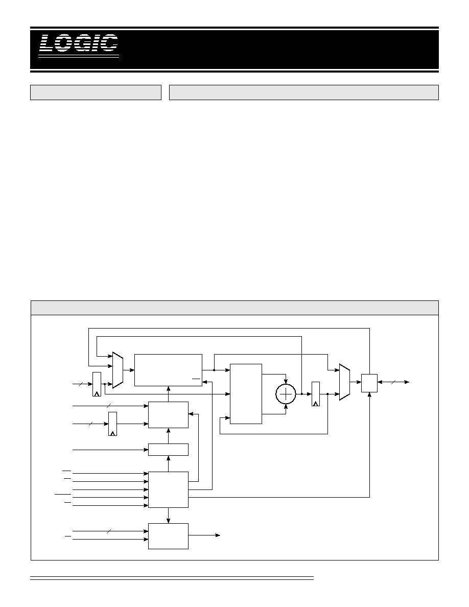
LF48410 B
LOCK
D
IAGRAM
CLK
ADDRESS
GENERATOR
CONTROL
WR
DIO
I/F
DIO
23-0
24
COUNTER
PIN
9-0
10
DIN
23-0
24
3
RAM ARRAY
DATA IN
DATA OUT
WR
ADDRESS
(TO ALL REGISTERS)
RD
UWS
START
FC
FUNCTION
DECODE
FCT
2-0
LD
MUX CONTROL SIGNALS
IOA
9-0
10
3
ADDER
INPUT
CONTROL

DEVICES INCORPORATED
LF48410
1024 x 24-bit Video Histogrammer
2
Video Imaging Products
08/08/2000≠LDS.48410-L
SIGNAL DEFINITIONS
Power
V
CC
and GND
+5 V power supply. All pins must be
connected.
Clock
CLK -- Master Clock
When operating in a synchronous
mode, the rising edge of CLK strobes
all enabled registers. CLK has no
effect when operating in an asynchro-
nous mode.
Inputs
PIN
9-0
-- Pixel Data Input
PIN
9-0
provides address information
to the memory array in Histogram,
Bin Accumulate, and Look Up Table
Modes. Data is latched on the rising
edge of CLK.
DIN
23-0
-- Data Input
In Bin Accumulate Mode, DIN
23-0
provides data to the internal summer
to be added to data already in the
memory array. In Look Up Table
Mode, DIN
23-0
is used to load the
memory array with the desired
values. In Delay Memory Mode, the
data to be delayed is input to the
memory array using DIN
23-0
, and in
Delay and Subtract Mode it also
provides data to be subtracted from
the delayed data. In all four modes,
DIN
23-0
is latched on the rising edge
of CLK.
IOA
9-0
-- Asynchronous Address Input
IOA
9-0
provides address information
to the memory array in Asynchronous
16 and 24 Modes.
FCT
2-0
-- Function Input
FCT
2-0
is used to put the LF48410 into
one of its eight modes of operation
(Table 1). Data is latched on the
rising edge of LD. To ensure proper
operation of the device, START must
be HIGH while changing modes, and
there must be at least one rising edge
of CLK between the rising edge of LD
and the falling edge of START.
Inputs/Outputs
DIO
23-0
-- Data Input/Output
In all synchronous modes, DIO
23-0
is
the 24-bit registered data output port.
In all asynchronous modes, DIO
23-0
is
both the data input and data output
port for the memory array.
Controls
START -- Device Enable
START is used to enable and disable
the synchronous modes of operation
(except for the Delay Memory and
Delay and Subtract Modes). The
synchronous mode sections explain
how START functions in each mode.
START has no effect in asynchronous
modes. Data is latched on the rising
edge of CLK. START must be held
HIGH when changing from one mode
to another. To ensure proper opera-
tion of the device, there must be at
least one rising edge of CLK between
the rising edge of LD and the falling
edge of START.
RD -- Read/Output Enable
In all synchronous modes, RD is used
as an output enable for DIO
23-0
.
When RD is LOW, DIO
23-0
is enabled
for output. When RD is HIGH, DIO
23-0
is placed in a high-impedance state.
In all asynchronous modes, RD is
used as a read enable for the memory
array (see asynchronous mode
sections for details).
WR -- Write Enable
In all asynchronous modes, WR is
used as a write enable for the
memory array (see asynchronous
mode sections for details). WR has
no effect in the synchronous modes.
UWS -- Upper Word Select
UWS is only used in Asynchronous 16
Mode. If UWS is LOW and a memory
write is performed, data on DIO
15-0
is
written to the lower 16 bits of the
addressed 24-bit word. If UWS is
LOW and a memory read is per-
formed, the lower 16 bits of the
addressed 24-bit word will be output
on DIO
15-0
. If UWS is HIGH and a
memory write is performed, data on
DIO
7-0
is written to the upper 8 bits of
the addressed 24-bit word. If UWS is
HIGH and a memory read is per-
formed, the upper 8 bits of the
addressed 24-bit word will be output
on DIO
7-0
.
FC -- Flash Clear
When FC is LOW, all memory array
locations and data path registers are
set to "0". To ensure that Flash Clear
functions properly, FC should not be
set LOW until START is HIGH
(synchronous modes) or WR is HIGH
(asynchronous modes).
LD -- Function Load Strobe
Data present on FCT
2-0
is latched into
the LF48410 on the rising edge of LD.
To ensure proper operation of the
device, there must be at least one
rising edge of CLK between the rising
edge of LD and the falling edge of
START.
FCT
2-0
MODE
0
0
0
Histogram
0
0
1
Histogram Accumulate
0
1
0
Delay and Subtract
0
1
1
Look Up Table
1
0
0
Bin Accumulate
1
0
1
Delay Memory
1
1
0
Asynchronous 24
1
1
1
Asynchronous 16
T
ABLE
1.
LF48410 M
ODES

DEVICES INCORPORATED
Video Imaging Products
3
LF48410
1024 x 24-bit Video Histogrammer
08/08/2000≠LDS.48410-L
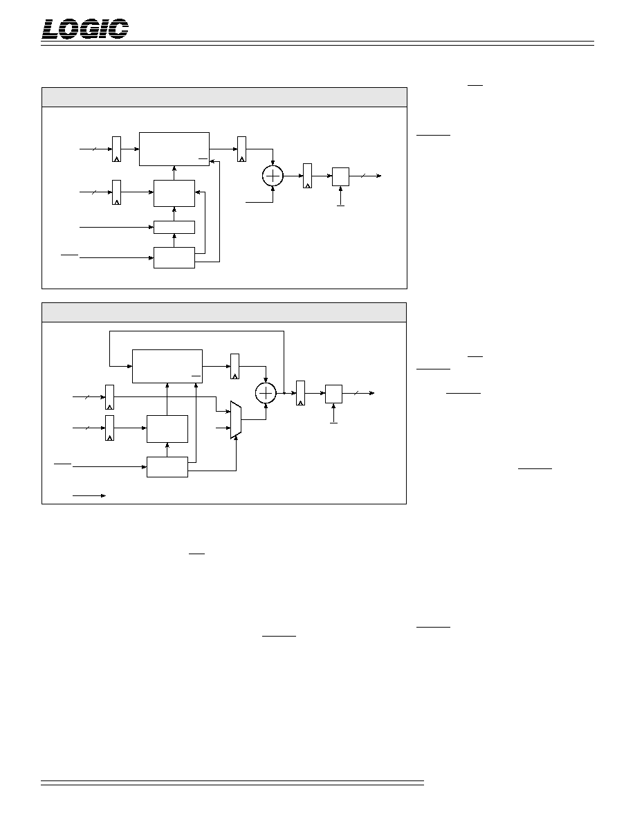
HISTOGRAM MODE
When the LF48410 is in this mode, the
chip is configured as shown in Figure
1. The memory array keeps track of
how many times a particular pixel
value is used in a video image. The
pixel value is input on PIN
9-0
and is
latched on the rising edge of CLK.
Data at the address defined by PIN
9-0
is read out of the memory array and
incremented by one. The data is then
written back to the memory array, in
the same location it was read from,
and is also output on DIO
23-0
(if RD is
LOW). As long as START is LOW,
the device will be enabled for Histo-
gram Mode. When START is HIGH,
the device will still read pixel values,
but the addres-sed data will not be
incremented. The unchanged data is
output on DIO
23-0
and is not written
back to the memory array (writing is
disabled). START is delayed inter-
nally three clock cycles to match the
latency of the address generator.
HISTOGRAM ACCUMULATE
MODE
When the LF48410 is in this mode, the
chip is configured as shown in Figure
2. This mode is used to calculate the
Cumulative Distribution Function of
a video image. Before this can be
done, the histogram of the image
must already be in the memory array.
The internal counter is used to
generate address data for the memory
array. Data at the address defined by
the counter is read out of the memory
array and added to the sum of the
data from all previous address
locations. This new value is written
back to the memory array, in the
same location where the last read
occurred, and is also output on
DIO
23-0
(if RD is LOW). After all
memory locations with histogram
data are accumulated, the memory
array will contain the Cumulative
Distribution Function.
After this mode is selected, the
internal counter and all data path
registers are reset to zero when
START is set LOW. Every rising edge
of CLK causes the counter to incre-
ment its output by one until the
counter reaches a value of 1023. At
this point, the counter will hold the
value of 1023 and writing to the
memory array will be disabled. As
long as START is LOW, the device
will be enabled for Histogram Accu-
mulate Mode. When START is HIGH,
the counter will still increment its
address values, but the addressed
data will not be added to anything.
The unchanged data is output on
DIO
23-0
and is not written back to the
memory array (writing is disabled).
START is delayed internally three
clock cycles to match the latency of
the address generator.
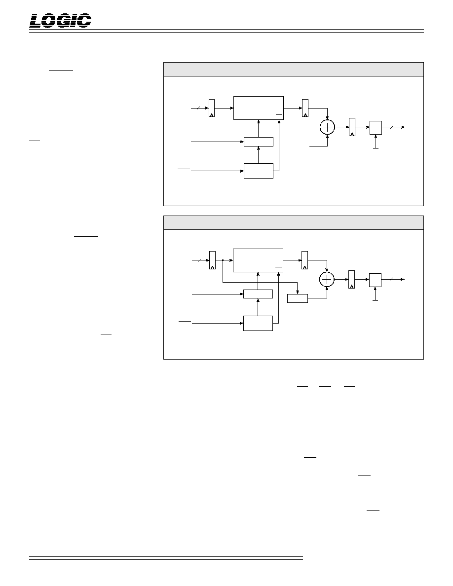
LOOK UP TABLE MODE
When the LF48410 is in this mode, the
chip is configured as shown in Figure
3. This mode is used to perform fixed
transformation functions on pixel
values. The transformation function
can be loaded into the memory array
in Look Up Table Write Mode,
Asynchronous 16/24 Mode, or
Histogram Accumulate Mode. In
Look Up Table Write Mode, data is
loaded into the memory array using
DIN
23-0
, CLK, and START. The
internal counter is used to generate
address data for the memory array.
When START goes LOW, the counter
is reset to zero. As long as START is
LOW, data on DIN
23-0
is latched on
the rising edge of CLK and loaded
F
IGURE
1.
H
ISTOGRAM
M
ODE
F
IGURE
2.
H
ISTOGRAM
A
CCUMULATE
M
ODE
RAM ARRAY
DATA IN
DATA OUT
ADDRESS
ADDRESS
GENERATOR
CONTROL
START
DIO
I/F
DIO
23-0
24
RD
COUNTER
CLK
(TO ALL REGISTERS)
WR
"0"
PIN
9-0
CLK
TO ALL REGISTERS
10
RAM ARRAY
DATA IN
DATA OUT
WR
ADDRESS
ADDRESS
GENERATOR
CONTROL
START
"0"
"1"
DIO
I/F
DIO
23-0
24
RD
DEVICES INCORPORATED
LF48410
1024 x 24-bit Video Histogrammer
4
Video Imaging Products
08/08/2000≠LDS.48410-L
into the memory array at the address
defined by the counter. The value
already in the memory array at that
address is output on DIO
23-0
(if RD is
LOW). Every rising edge of CLK
causes the counter to increment its
output by one until the counter
reaches a value of 1023. At this point,
the counter will hold the value of
1023 and writing to the memory array
will be disabled. DIN
23-0
is delayed
internally three clock cycles to match
the latency of the address generator.
In Asynchronous 16/24 Mode, data is
loaded into the memory array as
detailed in the asynchronous mode
sections. If the Cumulative Distribu-
tion Function is the desired transfor-
mation function, the memory array
will contain this data as soon as the
Histogram Accumulate function has
been completed.
Once the memory array contains the
desired data, the device needs to be
put in Look Up Table Read Mode by
setting START HIGH. In Look Up
Table Read Mode, pixel values are
input on PIN
9-0
and are latched on
the rising edge of CLK. Data at the
address defined by PIN
9-0
is read out
of the memory array and output on
DIO
23-0
(if RD is LOW). If Look Up
Table Write Mode was used to load
the memory array, it is important to
wait until the third clock cycle after
START goes HIGH to input data on
PIN
9-0
to insure that all data is
written into the memory array before
any reading is done.
BIN ACCUMULATE MODE
When the LF48410 is in this mode, the
chip is configured as shown in Figure
4. PIN
9-0
provides address data for
the memory array and is latched on
the rising edge of CLK. Data at the
address defined by PIN
9-0
is read out
of the memory array and added to
the data on DIN
23-0
. This new value
is written back to the memory array,
in the same location where the last
read occured, and is also output on
DIO
23-0
(if RD is LOW). As long as
START is LOW, the device will be
enabled for Bin Accumulate Mode.
When START is HIGH, the device will
still read address values on PIN
9-0
, but
the addressed data will not be added
to anything. The unchanged data will
be output on DIO
23-0
and is not
written back to the memory array
(writing is disabled). START and
DIN
23-0
are delayed internally three
clock cycles to match the latency of
the address generator.
DELAY MEMORY MODE
When the LF48410 is in this mode, the
chip is configured as shown in Figure
5. This mode allows the device to
function as a row buffer. The internal
counter is used to generate address
data for the memory array. When
START goes LOW, the counter is
reset to zero. Delay length (row
length) is determined by reseting the
counter every N≠4 clock cycles, where
N is the number of delays. For
F
IGURE
3.
L
OOK
U
P
T
ABLE
M
ODE
F
IGURE
4.
B
IN
A
CCUMULATE
M
ODE
CLK
ADDRESS
GENERATOR
CONTROL
START
DIO
I/F
DIO
23-0
24
RD
COUNTER
PIN
9-0
10
DIN
23-0
24
3
"0"
RAM ARRAY
DATA IN
DATA OUT
WR
ADDRESS
(TO ALL REGISTERS)
NOTE: NUMBER IN REGISTER INDICATES
NUMBER OF PIPELINE DELAYS.
PIN
9-0
CLK
TO ALL REGISTERS
10
RAM ARRAY
DATA IN
DATA OUT
ADDRESS
ADDRESS
GENERATOR
CONTROL
START
"0"
DIO
I/F
DIO
23-0
24
RD
DIN
23-0
24
3
NOTE: NUMBER IN REGISTER INDICATES
NUMBER OF PIPELINE DELAYS.
WR
DEVICES INCORPORATED
Video Imaging Products
5
LF48410
1024 x 24-bit Video Histogrammer
08/08/2000≠LDS.48410-L
example, to set the number of delays
to 10, START would have to be set
LOW every 6 cycles. The maximum
delay length is 1029 and the minimum
delay length is 6. Data on DIN
23-0
is latched on the rising edge of
CLK and loaded into the memory
array at the address defined by the
counter. Data is output on DIO
23-0
(if
RD is LOW). If the counter reaches
the value of 1023, the counter will
hold this value and writing to the
memory array will be disabled.
DELAY AND SUBTRACT MODE
When the LF48410 is in this mode, the
chip is configured as shown in Figure 6.
The internal counter is used to gener-
ate address data for the memory
array. When START goes LOW, the
counter is reset to zero. Delay length
(row length) is determined by
reseting the counter every N≠4 clock
cycles, where N is the number of
delays. The maximum delay length is
1029 and the minimum delay length
is 6. Data on DIN
23-0
is latched on the
rising edge of CLK and loaded into
the memory array at the address
defined by the counter. Data is
output on DIO
23-0
(if RD is LOW).
Before data read from the memory
array is output to DIO
23-0
, input data
is subtracted from it according to the
following formula: OUT
C
= D
(C≠N+1)
≠
D
(C≠3)
. OUT
C
is the data sent to the
output port (DIO
23-0
) on clock cycle C.
D
(C≠N+1)
is the data latched into the
device on clock cycle C≠N+1, and D
(C-
3)
is the data latched into the device on
clock cycle C≠3. N is the number of
delays. For example, to determine
what will be output on DIO
23-0
on
clock cycle 12 when the device is set
for 10 delays, set C=12 and N=10 to
obtain: OUT
12
= D
3
≠ D
9
. If the
counter reaches the value of 1023, the
counter will hold this value and
writing to the memory array will be
disabled.
ASYNCHRONOUS 16 MODE
When the LF48410 is in this mode, the
chip is configured as shown in Figure 7.
This mode allows the device to
function as an asynchronous single
port RAM. Each 24-bit memory
location is split into two parts, the
lower 16 bits and the upper 8 bits.
IOA
9-0
addresses the 24-bit memory
locations, and UWS addresses the
lower 16 or upper 8 bits of those
locations. If UWS is LOW, the lower
16 bits of the 24-bit memory location
are addressed. If UWS is HIGH, the
upper 8 bits are addressed. Address
data on IOA
9-0
and UWS is latched
into the device on the falling edge of
RD or WR. If RD latches the address
data, a memory read is performed.
Data at the specified address is
output on DIO
15-0
(if UWS was
latched LOW) or DIO
7-0
(if UWS was
latched HIGH). If UWS was latched
LOW/HIGH, DIO
16-23
/DIO
8-23
will
output zeros during a memory read.
If WR latches the address data, a
memory write is performed. After
the falling edge of WR latches the
address, data on DIO
15-0
(if UWS was
latched LOW) or DIO
7-0
(if UWS was
latched HIGH) is written to the RAM
on the rising edge of WR.
F
IGURE
6.
D
ELAY
A
ND
S
UBTRACT
M
ODE
F
IGURE
5.
D
ELAY
M
EMORY
M
ODE
RAM ARRAY
DATA IN
DATA OUT
ADDRESS
CONTROL
START
DIO
I/F
DIO
23-0
24
RD
CLK
COUNTER
(TO ALL REGISTERS)
DIN
23-0
24
3
NOTE: NUMBER IN REGISTER INDICATES
NUMBER OF PIPELINE DELAYS.
≠DIN
23-0
WR
RAM ARRAY
DATA IN
DATA OUT
ADDRESS
CONTROL
START
"0"
DIO
I/F
DIO
23-0
24
RD
CLK
COUNTER
(TO ALL REGISTERS)
DIN
23-0
24
3
NOTE: NUMBER IN REGISTER INDICATES
NUMBER OF PIPELINE DELAYS.
WR