DEVICES INCORPORATED
1
LF9501
Programmable Line Buffer
08/16/2000≠LDS.9501-H
Video Imaging Products
u
u
u
u
u
50 MHz Maximum Operating
Frequency
u
u
u
u
u Programmable Buffer Length from
2 to 1281 Clock Cycles
u
u
u
u
u 10-bit Data Inputs and Outputs
u
u
u
u
u Data Delay and Data Recirculation
Modes
u
u
u
u
u Supports Positive or Negative Edge
System Clocks
u
u
u
u
u Expandable Data Word Width or
Buffer Length
u
u
u
u
u Replaces Harris HSP9501
u
u
u
u
u 44-pin PLCC, J-Lead
FEATURES
DESCRIPTION
LF9501
Programmable Line Buffer
DEVICES INCORPORATED
The LF9501 is a high-speed, 10-bit
programmable line buffer. Some
applications the LF9501 is useful for
include sample rate conversion, data
time compression/expansion, soft-
ware controlled data alignment, and
programmable serial data shifting. By
using the MODSEL pin, two different
modes of operation can be selected:
delay mode and data recirculation
mode. The delay mode provides a
minimum of 2 to a maximum of 1281
clock cycles of delay between the
input and output of the device. The
data recirculation mode provides a
feedback path from the data output to
the data input for use as a program-
mable circular buffer.
By using the length control input
(LC
10-0
) and the length control enable
(LCEN) the length of the delay buffer
or amount of recirculation delay can
be programmed. Providing a delay
value on the LC
10-0
inputs and driving
LCEN LOW will load the delay value
into the length control register on the
next selected clock edge. Two regis-
ters, one preceeding the program-
mable delay RAM and one following,
are included in the delay path. There-
fore, the programmed delay value
should equal the desired delay minus
2. This consequently means that the
value loaded into the length control
register must range from 0 to 1279 (to
provide an overall range of 2 to 1281).
The active edge of the clock input,
either positive or negative edge, can
be selected with the clock select
(CLKSEL) input. All timing is based
on the active clock edge selected by
CLKSEL. Data can be held tempo-
rarily by using the clock enable
(CLKEN) input.
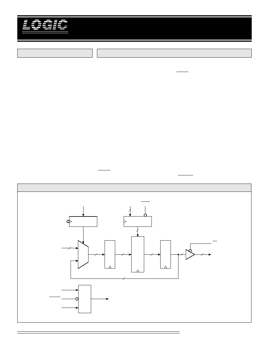
LF9501 B
LOCK
D
IAGRAM
REGISTER
MUX
PROGRAMMABLE
DELAY RAM
REGISTER
DI
9-0
10
10
10
10
10
10
10
MODSEL
CLOCK
GENERATOR
CLKSEL
CLKEN
CLK
OE
REGISTER
LCO
10-0
LCEN
11
11
TO ALL REGISTERS
REGISTER
DO
9-0

DEVICES INCORPORATED
LF9501
Programmable Line Buffer
2
08/16/2000≠LDS.9501-H
Video Imaging Products
Outputs
DO
9-0
-- Data Output
The 10-bit data output appears on
DO
9-0
on the Nth clock cycle, where N
is the overall delay (desired delay).
Controls
LCEN -- Length Control Enable
When LCEN is driven LOW, the next
active clock edge will cause the
loading of the delay value present at
the LC
10-0
input.
OE -- Output Enable
The Output Enable controls the state
of DO
9-0
. Driving OE LOW enables
the output port. When OE is HIGH,
DO
9-0
is placed in a high-impedance
state. The internal transfer of data is
not affected by this control.
MODSEL -- Mode Select
The Mode Select pin is used to choose
the desired mode of operation: data
delay mode or data recirculation
mode. Driving MODSEL LOW places
the device in the delay mode. The
device operates as a programmable
pipeline register. New data from the
DI
9-0
input is loaded on every active
edge of CLK. Driving MODSEL
HIGH places the device in the data
recirculation mode. The device
operates as a programmable circular
buffer. The output of the device is
routed back to the input. MODSEL
may be changed during device
operation (synchronously), however,
the required setup and hold times,
with respect to CLK, must be met.
SIGNAL DEFINITIONS
Power
V
CC
and GND
+5 V power supply. All pins must be
connected.
Clock
CLK -- Master Clock
The active edge of CLK, selected by
CLKSEL, strobes all registers. All
timing specifications are referenced to
the active edge of CLK.
Inputs
DI
9-0
-- Data Input
10-bit data, from the data input, is
latched into the device on the active
edge of CLK when MODSEL is LOW.
LC
10-0
-- Length Control Input
The 11-bit value is used to specify the
length of the delay buffer, between
DI
9-0
and DO
9-0
, or the amount of
recirculation delay. An integer value
ranging from 0 to 1279 is used to
select a delay ranging from 2 to 1281
clock cycles. The value placed on the
LC
10-0
inputs is equal to the desired
delay minus 2. The data presented on
LC
10-0
is loaded into the device on the
active edge of CLK, selected by
CLKSEL, in conjunction with LCEN
being driven LOW.
CLKSEL -- Clock Select
The CLKSEL control allows the
selection of the active edge of CLK. A
LOW on CLKSEL selects negative-
edge triggering of the device. Driving
CLKSEL HIGH selects positive-edge
triggering. All timing specifications
are referrenced to the selected active
edge of CLK.
CLKEN -- Clock Enable
The Clock Enable control enables and
disables the CLK input. Driving
CLKEN LOW enables CLK and causes
the device to operate in a normal
fashion. When CLKEN is HIGH, CLK
is disabled and the device will hold all
internal operations and data. CLKEN
may be changed during device
operation (synchronously), however,
the required setup and hold times,
with respect to CLK, must be met.
The changing of CLKEN takes effect
on the active edge of CLK following
the edge in which it was latched.

DEVICES INCORPORATED
3
LF9501
Programmable Line Buffer
08/16/2000≠LDS.9501-H
Video Imaging Products
Storage temperature ........................................................................................................... ≠65∞C to +150∞C
Operating ambient temperature ........................................................................................... ≠55∞C to +125∞C
V
CC
supply voltage with respect to ground ............................................................................ ≠0.5 V to +7.0 V
Input signal with respect to ground ............................................................................... ≠0.5 V to V
CC
+ 0.5 V
Signal applied to high impedance output ...................................................................... ≠0.5 V to V
CC
+ 0.5 V
Output current into low outputs ............................................................................................................. 25 mA
Latchup current ............................................................................................................................... > 400 mA
M
AXIMUM
R
ATINGS
Above which useful life may be impaired (Notes 1, 2, 3, 8)
Symbol
Parameter
Test Condition
Min
Typ
Max
Unit
V
OH
Output High Voltage
V
CC
= Min., I
OH
= ≠4.0 mA
2.4
V
V
OL
Output Low Voltage
V
CC
= Min., I
OL
= 4.0 mA
0.4
V
V
IH
Input High Voltage
2.0
V
CC
V
V
IL
Input Low Voltage
(Note 3)
0.0
0.8
V
I
IX
Input Current
Ground
V
IN
V
CC
(Note 12)
±
10
µA
I
OZ
Output Leakage Current
Ground
V
OUT
V
CC
(Note 12)
±
10
µA
I
CC1
V
CC
Current, Dynamic
(Notes 5, 6)
125
mA
I
CC2
V
CC
Current, Quiescent
(Note 7)
500
µA
C
IN
Input Capacitance
T
A
= 25∞C, f = 1 MHz
10
pF
C
OUT
Output Capacitance
T
A
= 25∞C, f = 1 MHz
10
pF
E
LECTRICAL
C
HARACTERISTICS
Over Operating Conditions (Note 4)
O
PERATING
C
ONDITIONS
To meet specified electrical and switching characteristics
Mode
Temperature Range (Ambient)
Supply Voltage
Active Operation, Commercial
0∞C to +70∞C
4.75 V
V
CC
5.25 V

DEVICES INCORPORATED
LF9501
Programmable Line Buffer
4
08/16/2000≠LDS.9501-H
Video Imaging Products
1234567890
1234567890
1234567890
1234567890
1234567890
1234567890
1234567890
1234567890
1234567890
1234567890
1234567890
1234567890
1234567890
1234567890
1234567890
1234567890
1234567890
1234567890
1234567890
1234567890
1234567890
1234567890
1234567890
1234567890
1234567890
1234567890
1234567890
1234567890
1234567890
1234567890
1234567890
1234567890
1234567890
1234567890
1234567890
1234567890
1234567890
1234567890
1234567890
1234567890
1234567890
1234567890
1234567890
1234567890
1234567890
1234567890
1234567890
1234567890
1234567890
1234567890
1234567890
1234567890
1234567890
1234567890
1234567890
1234567890
1234567890
1234567890
12345678901234567890
12345678901234567890
12345678901234567890
12345678901234567890
12345678901234567890
12345678901234567890
12345678901234567890
12345678901234567890
12345678901234567890
12345678901234567890
12345678901234567890
12345678901234567890
12345678901234567890
12345678901234567890
12345678901234567890
12345678901234567890
12345678901234567890
12345678901234567890
12345678901234567890
12345678901234567890
12345678901234567890
12345678901234567890
12345678901234567890
12345678901234567890
12345678901234567890
12345678901234567890
12345678901234567890
12345678901234567890
12345678901234567890
12345678901234567890
12345678901234567890
12345678901234567890
12345678901234567890
12345678901234567890
12345678901234567890
12345678901234567890
12345678901234567890
12345678901234567890
12345678901234567890
12345678901234567890
12345678901234567890
12345678901234567890
12345678901234567890
12345678901234567890
12345678901234567890
12345678901234567890
12345678901234567890
12345678901234567890
12345678901234567890
12345678901234567890
12345678901234567890
12345678901234567890
12345678901234567890
12345678901234567890
12345678901234567890
12345678901234567890
12345678901234567890
12345678901234567890
LF9501≠
40*
31*
25
20
15*
Symbol
Parameter
Min Max Min Max Min Max Min Max Min Max
t
CYC
Cycle Time
40
31
25
20
15
t
PW
Clock Pulse Width
15
12
10
8
6
t
DS
Data Input Setup Time
12
10
8
6
5
t
DH
Data Input Hold Time
2
2
2
2
0
t
ES
Clock Enable to Clock Setup Time
12
10
8
6
5
t
EH
Clock Enable to Clock Hold Time
2
2
2
2
0
t
LS
Length Control Input Setup Time
13
10
8
6
5
t
LH
Length Control Input Hold Time
2
2
2
2
0
t
LES
Length Control Enable to Clock Setup Time
13
10
8
6
5
t
LEH
Length Control Enable to Clock Hold Time
2
2
2
2
0
t
MS
Mode Select Setup Time
13
10
8
6
5
t
MH
Mode Select Hold Time
2
2
2
2
0
t
OUT
Clock to Data Out
22
16
15
14
10
t
OH
Output Hold Time
(Note 8)
4
4
4
4
4
t
ENA
Three-State Output Enable Delay
(Note 11)
25
20
15
14
12
t
DIS
Three-State Output Disable Delay
(Note 11)
25
24
15
14
12
C
OMMERCIAL
O
PERATING
R
ANGE
(0∞C to +70∞C)
Notes 9, 10 (ns)
SWITCHING CHARACTERISTICS
*When CLKSEL is HIGH, assume CLK is inverted.
F
UNCTIONAL
T
IMING
-- CLKSEL LOW
CLK*
t
CYC
t
PW
t
PW
MODSEL
t
MH
t
DS
t
DH
DI
9-0
DO
9-0
OE
t
DIS
t
ENA
t
OUT
t
OH
t
MS
HIGH IMPEDANCE
123456789012345678901234
123456789012345678901234
123456789012345678901234
*D
ISCONTINUED
S
PEED
G
RADE

DEVICES INCORPORATED
5
LF9501
Programmable Line Buffer
08/16/2000≠LDS.9501-H
Video Imaging Products
1234567890
1234567890
1234567890
1234567890
1234567890
1234567890
1234567890
1234567890
1234567890
1234567890
1234567890
1234567890
1234567890
1234567890
1234567890
1234567890
1234567890
1234567890
1234567890
1234567890
1234567890
1234567890
1234567890
1234567890
1234567890
1234567890
1234567890
1234567890
1234567890
1234567890
1234567890
1234567890
1234567890
1234567890
1234567890
1234567890
1234567890
1234567890
1234567890
1234567890
1234567890
1234567890
1234567890
1234567890
1234567890
1234567890
1234567890
1234567890
1234567890
1234567890
1234567890
1234567890
1234567890
1234567890
1234567890
1234567890
1234567890
12345678901234567890
12345678901234567890
12345678901234567890
12345678901234567890
12345678901234567890
12345678901234567890
12345678901234567890
12345678901234567890
12345678901234567890
12345678901234567890
12345678901234567890
12345678901234567890
12345678901234567890
12345678901234567890
12345678901234567890
12345678901234567890
12345678901234567890
12345678901234567890
12345678901234567890
12345678901234567890
12345678901234567890
12345678901234567890
12345678901234567890
12345678901234567890
12345678901234567890
12345678901234567890
12345678901234567890
12345678901234567890
12345678901234567890
12345678901234567890
12345678901234567890
12345678901234567890
12345678901234567890
12345678901234567890
12345678901234567890
12345678901234567890
12345678901234567890
12345678901234567890
12345678901234567890
12345678901234567890
12345678901234567890
12345678901234567890
12345678901234567890
12345678901234567890
12345678901234567890
12345678901234567890
12345678901234567890
12345678901234567890
12345678901234567890
12345678901234567890
12345678901234567890
12345678901234567890
12345678901234567890
12345678901234567890
12345678901234567890
12345678901234567890
12345678901234567890
SWITCHING CHARACTERISTICS
C
LOCK
E
NABLE
T
IMING
-- CLKSEL LOW
CLK*
t
PW
CLKEN
t
MH
t
ES
t
ES
INTERNAL
CLOCK
L
ENGTH
C
ONTROL
T
IMING
-- CLKSEL LOW
CLK*
t
LEH
LCEN
t
MH
t
LES
LC
10-0
t
LS
t
LH
*When CLKSEL is HIGH, assume CLK is inverted.
LF9501≠
40*
31*
25
20
15*
Symbol
Parameter
Min Max Min Max Min Max Min Max Min Max
t
CYC
Cycle Time
40
31
25
20
15
t
PW
Clock Pulse Width
15
12
10
8
6
t
DS
Data Input Setup Time
12
10
8
6
5
t
DH
Data Input Hold Time
2
2
2
2
0
t
ES
Clock Enable to Clock Setup Time
12
10
8
6
5
t
EH
Clock Enable to Clock Hold Time
2
2
2
2
0
t
LS
Length Control Input Setup Time
13
10
8
6
5
t
LH
Length Control Input Hold Time
2
2
2
2
0
t
LES
Length Control Enable to Clock Setup Time
13
10
8
6
5
t
LEH
Length Control Enable to Clock Hold Time
2
2
2
2
0
t
MS
Mode Select Setup Time
13
10
8
6
5
t
MH
Mode Select Hold Time
2
2
2
2
0
t
OUT
Clock to Data Out
22
16
15
14
10
t
OH
Output Hold Time
(Note 8)
4
4
4
4
4
t
ENA
Three-State Output Enable Delay
(Note 11)
25
20
15
14
12
t
DIS
Three-State Output Disable Delay
(Note 11)
25
24
15
14
12
C
OMMERCIAL
O
PERATING
R
ANGE
(0∞C to +70∞C)
Notes 9, 10 (ns)
123456789012345678901234
123456789012345678901234
123456789012345678901234
*D
ISCONTINUED
S
PEED
G
RADE