F E A T U R E S
150 MHz operation at 1.2V
2 high-speed serial/TDM ports
(T1/E1 framer, H.100/H.110 bit
stream compatible)
Low power dissipation (50mW
typical at 150 MHz)
Sleep power mode consumes
<20mW/MHz
48K words on-chip RAM
8-channel DMA controller
On-board PLL for clock generation
2 on-board timers
8-bit host processor interface with
hardware byte pack/unpack
IEEE 1149.1-compliant JTAG port for
in-system debug
144 LBGA Package (7mm x 7mm)
Available in 120 or 150 MHz versions
B E N E F I T S
300 MMAC sustained DSP
performance at 150 MHz
Direct interfacing to standard
telecommunications interfaces,
reducing system cost
Low power per voice or audio channel
Suitable for very low power applications
High data throughput without
processor overhead
Flexibility to optimize power
consumption
High data bandwidth to off-chip devices
Simple interfacing to industry-
standard micros
Low overhead on chip debug
Ideal for low-cost VoIP designs
O V E R V I E W
The LSI403US is an extremely low power 16-bit fixed-point digital signal processor
(DSP) based on the LSI Logic ZSP400 DSP core, running less than 250
µW per
DSP MIPS (MMAC). The device is packaged in an Ultra-sleek 144-pin LBGA
package which is 7mm x 7mm in size. LSI403US is designed for consumer hand-
held applications such as VoWiFi and Audio. The LSI403US is capable of a
maximum clock rate of 150 MHz for 600 MIPS peak performance and sustained
effective throughput of 300 DSP MIPS (MMACs). The device is also software com-
patible with all other products in the ZSP architecture, and offers an unrivaled com-
bination of code density, performance and ease of use.
M E M O R Y
The internal memory structure of the LSI403US comprises of 16K words of instruction
memory, 16K words of data memory, 16K words of configurable memory for
instruction or data, 1K words of memory for bootloading and interrupt support
and peripherals.
D M A
The DMA controller of the LSI403US supports zero-overhead instruction or data
transfers to or from the entire 48K words of internal RAM to the memory interface
unit, host processor interface, or a serial port. The eight DMA channels are seg-
mented between four "indexed" and four "non-indexed" channels. Indexed channels
have the ability to buffer data from either of the serial TDM interfaces, and non-indexed
channels perform sequential accesses to or from internal memory. All DMA channels
feature an auto-reload capability to restart transfers with no processor overhead.
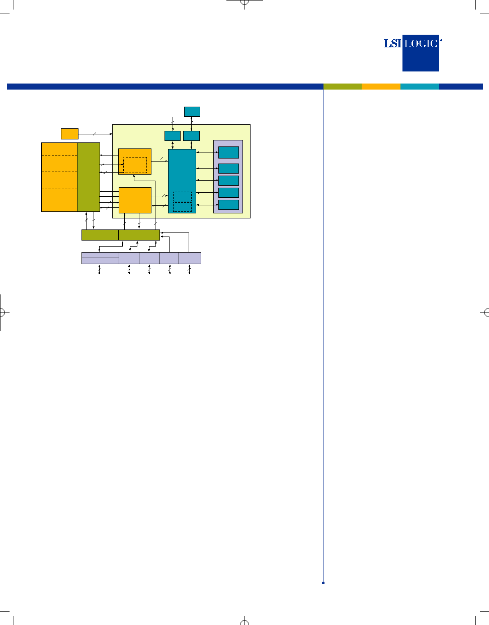
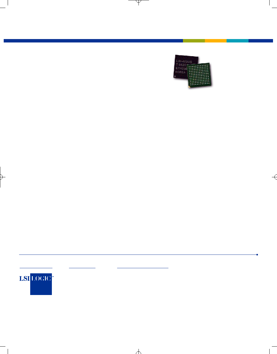
LSI403US Digital Signal Processor
Ultra-Sleek Package (7mm x 7mm)
HPI
Execution Unit
rdA
wrA
DO
DI
64
32
64
64
Interrupts
ICU
PLL
DMA Controller
Instruction Unit
Instruction
Cache
Data Unit
Pipeline Control
Unit
Register
File
ALU
ALU
MAC
MAC
HPI = Host Processor Interface
PIO = Programmable I/O
External Memory
Interface Unit (MXU)
32
16
16
PIO(4)
64
32
A
DO
Timer0
Timer1
ICU = Interrupt Control Unit
DEU = Device Emulation Unit
DI
32
Load/Store Buffer
XBus
16/32
16
16
XBus = External Bus
JTAG
DEU
Serial
Port 0
Serial
Port 1
6
5
Internal
Memory
Controller
Boot RAM
1K x 16
Instruction Memory
16K x 16
Configurable Memory
16K x 16
Data Memory
16K x 16
8
8
14
4
PLL = Phase-Locked Loop
5
Figure 1.
LSI403US
Functional Block
Diagram
T I M E R S
The LSI403US has two identical 16-bit on board timers for
real-time interrupt generation. Each timer is fully program-
mable, and has a 6-bit prescaler and interrupt capability.
The timers can automatically reload with the initial count so
that periodic interrupts can be generated.
T D M S E R I A L P O R T S
The LSI403US provides two identical synchronous serial
ports that support 8- or 16-bit active or passive transfers,
which can be either burst or continuous, with a maximum
clock speed of one-half the processor clock. Both serial ports
support m- and A-law hardware companding and provide
the programmable feature of a TDM (time division multiplex)
mode that is compatible with T1/E1 framers or the local
serial bus of H.100/H.110 interface devices. The TDM
mode can also be used to establish a serial multiprocessor
communication link with only three signals.
H O S T P R O C E S S O R I N T E R F A C E ( H P I )
The Host Processor Interface, or HPI, is an asynchronous
8-bit parallel port that is used to interface with off-chip
devices. It is compatible with both Motorola and Intel style
memory interfaces, and supports word transfers. The maxi-
mum transfer rate for the HPI is one-third of the processor
clock frequency. The HPI includes hardware support to
pack/unpack bytes to/from 16-bit words, removing the
overhead of this task from the ZSP400 core.
LSI Logic Corporation
North American Headquarters
Milpitas, CA
Tel: 866-574-5741
North America
Milpitas, CA
Tel: 1-408-490-8000
Fax: 1-408-490-8590
Quebec, Canada
Tel: 1-514-426-5011
Fax: 1-514-426-7119
Europe
European Headquarters
United Kingdom
Tel: 44-1344-413200
Fax: 44-1293-651119
Hong Kong
Kowloon Tong, Hong Kong
Tel: 852-2192-1789
Fax: 852-2511-6939
China
Beijing, China
Tele: 86-10-626-38296
Fax: 86-10-626-38322
Chengdu, China
Tel: 86-28-667-8831
Fax: 86-28-667-8054
Japan
Tokyo, Japan
Tel: 81-3-5463-7821
Fax: 81-3-5463-7820
Korea
Seoul, Korea
Tele: 82-2-528-3400
Fax: 82-2-528-2250
Taiwan
Taipei, Taiwan
Tel: 866-2-2718-7828
Fax:866-2-2718-8869
LSI Logic, the LSI Logic logo design,
ZSP and ZOpen are trademarks or
registered trademarks of LSI Logic
Corporation. All other brand and
product names may be trademarks
of their respective companies.
LSI Logic Corporation reserves the
right to make changes to any prod-
ucts and services herein at any time
without notice. LSI Logic does not
assume any responsibility or liability
arising out of the application or use
of any product or service described
herein, except as expressly agreed to
in writing by LSI Logic; nor does the
purchase, lease, or use of a product
or service from LSI Logic convey a
license under any patent rights, copy-
rights, trademark rights, or any other
of the intellectual property rights of
LSI Logic or of third parties.
Copyright ©2005 by LSI Logic
Corporation. All rights reserved.
Order No. R20113
0705.LR/CE - Printed in USA
LSI403US: Digital Signal Processor - Ultra-Sleek Package (7mm x 7mm)
For more information and sales office locations, please visit the LSI Logic web sites at:
www.lsilogic.com
www.zsp.com
http://lsilogic.com/contacts