LESHAN RADIO COMPANY, LTD.
UN2211LT1 Series
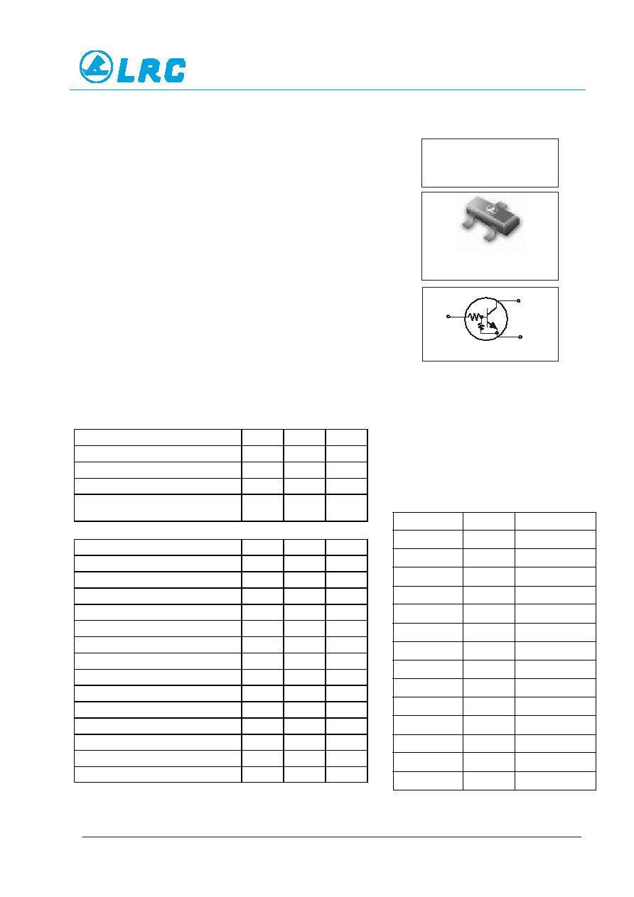
PIN 1
BASE
(INPUT)
PIN 3
COLLECTOR
(OUTPUT)
PIN 2
EMITTER
(GROUND)
R
1
R
2
1
3
2
SOT≠23 (TO≠236AB)
LMUN2211LT1
SERIES
Bias Resistor Transistor
NPN Silicon Surface Mount Transistor
with Monolithic Bias Resistor Network
This new series of digital transistors is designed to replace a single
device and its external resistor bias network. The BRT (Bias Resistor
Transistor) contains a single transistor with a monolithic bias network
consisting of two resistors; a series base resistor and a base-emitter
resistor. The BRT eliminates these individual components by
integrating them into a single device. The use of a BRT can reduce
both system cost and board space. The device is housed in the SOT-23
package which is designed for low power surface mount applications.
∑
Simplifies Circuit Design
∑
Reduces Board Space and Component Count
∑
The SOT-23 package can be soldered using wave or reflow. The
modified gull-winged leads absorb thermal stress during soldering
eliminating the possibility of damage to the die.
∑
Available in 8 mm embossed tape and reel. Use the Device
Number to order the 7 inch/3000 unit reel. Replace "T1" with
"T3" in the Device Number to order the13 inch/10,000 unit reel.
MAXIMUM RATINGS
(TA = 25
∞
C unless otherwise noted)
Rating
Symbol
Value
Unit
Collector-Base Voltage
V
CBO
50
Vdc
Collector-Emitter Voltage
V
CEO
50
Vdc
Collector Current
I
C
100
mAdc
Total Power Dissipation @ T
A
= 25
∞
C
(Note 1.) Derate above 25
∞
C
P
D
*
246
1.5
mW
∞
C/W
DEVICE MARKING AND RESISTOR VALUES
Device
Marking
R1(K)
R2(K)
LMUN2211LT1
A8A
10
10
LMUN2212LT1
A8B
22
22
LMUN2213LT1
A8C
47
47
LMUN2214LT1
A8D
10
47
LMUN2215LT1
A8E
10
LMUN2216LT1
A8F
4.7
LMUN2230LT1
A8G
1.0
1.0
LMUN2231LT1
A8H
2.2
2.2
LMUN2232LT1
A8J
4.7
4.7
LMUN2233LT1
A8K
4.7
47
LMUN2234LT1
A8L
22
47
LMUN2235LT1
A8M
2.2
47
LMUN2238LT1
A8R
2.2
LMUN2241LT1
A8U
100
1. Device mounted on a FR-4 glass epoxy printed circuit board using the
minimum recommended footprint.
Device
Package
Shipping
ORDERING INFORMATION
LMUN2211LT1G
SOT≠23
3000/Tape & Reel
LMUN2212LT1G
SOT≠23
3000/Tape & Reel
LMUN2213LT1G
SOT≠23
3000/Tape & Reel
LMUN2214LT1G
SOT≠23
3000/Tape & Reel
LMUN2215LT1G
SOT≠23
3000/Tape & Reel
LMUN2216LT1G
SOT≠23
3000/Tape & Reel
LMUN2230LT1G
SOT≠23
3000/Tape & Reel
LMUN2231LT1G
SOT≠23
3000/Tape & Reel
LMUN2232LT1G
SOT≠23
3000/Tape & Reel
LMUN2233LT1G
SOT≠23
3000/Tape & Reel
LMUN2234LT1G
SOT≠23
3000/Tape & Reel
LMUN2235LT1G
SOT≠23
3000/Tape & Reel
LMUN2238LT1G
SOT≠23
3000/Tape & Reel
LMUN2241LT1G
SOT≠23
3000/Tape & Reel
LMUN2211S-1/11
∑
Pb-Free Package May be Available.
The G-Suffix Denotes a Pb-Free
Lead Finish
LESHAN RADIO COMPANY, LTD.
LMUN2211S≠2/11
LMUN2211LT1 Series
THERMAL CHARACTERISTICS
Rating
Symbol
Value
Unit
Thermal Resistance ≠ Junction-to-Ambient (Note 1.)
R
JA
508
∞
C/W
Operating and Storage Temperature Range
T
J
, T
stg
≠55 to +150
∞
C
Maximum Temperature for Soldering Purposes,
Time in Solder Bath
T
L
260
10
∞
C
Sec
ELECTRICAL CHARACTERISTICS
(TA = 25
∞
C unless otherwise noted)
Characteristic
Symbol
Min
Typ
Max
Unit
OFF CHARACTERISTICS
Collector-Base Cutoff Current (V
CB
= 50 V, I
E
= 0)
I
CBO
≠
≠
100
nAdc
Collector-Emitter Cutoff Current (V
CE
= 50 V, I
B
= 0)
I
CEO
≠
≠
500
nAdc
Emitter-Base Cutoff Current
LMUN2211LT1
(V
EB
= 6.0 V, I
C
= 0)
LMUN2212LT1
LMUN2213LT1
LMUN2214LT1
LMUN2215LT1
LMUN2216LT1
LMUN2230LT1
LMUN2231LT1
LMUN2232LT1
LMUN2233LT1
LMUN2234LT1
LMUN2235LT1
LMUN2238LT1
LMUN2241LT1
I
EBO
≠
≠
≠
≠
≠
≠
≠
≠
≠
≠
≠
≠
≠
≠
≠
≠
≠
≠
≠
≠
≠
≠
≠
≠
≠
≠
≠
≠
0.5
0.2
0.1
0.2
0.9
1.9
4.3
2.3
1.5
0.18
0.13
0.2
4.0
0.1
mAdc
Collector-Base Breakdown Voltage (I
C
= 10
µ
A, I
E
= 0)
V
(BR)CBO
50
≠
≠
Vdc
Collector-Emitter Breakdown Voltage (Note 2.), (I
C
= 2.0 mA, I
B
= 0)
V
(BR)CEO
50
≠
≠
Vdc
ON CHARACTERISTICS
(Note 2.)
DC Current Gain
LMUN2211LT1
(V
CE
= 10 V, I
C
= 5.0 mA)
LMUN2212LT1
LMUN2213LT1
LMUN2214LT1
LMUN2215LT1
LMUN2216LT1
LMUN2230LT1
LMUN2231LT1
LMUN2232LT1
LMUN2233LT1
LMUN2234LT1
LMUN2235LT1
LMUN2238LT1
LMUN2241LT1
h
FE
35
60
80
80
160
160
3.0
8.0
15
80
80
80
160
160
60
100
140
140
350
350
5.0
15
30
200
150
140
350
350
≠
≠
≠
≠
≠
≠
≠
≠
≠
≠
≠
≠
≠
≠
Collector-Emitter Saturation Voltage (I
C
= 10 mA, I
B
= 0.3 mA)
(I
C
= 10 mA, I
B
= 5 mA) LMUN2230LT1/LMUN2231LT1
(I
C
= 10 mA, I
B
= 1 mA) LMUN2215LT1/LMUN2216LT1
LMUN2232LT1/LMUN2233LT1/LMUN2234LT1/
LMUN2235LT1/LMUN2238LT1
V
CE(sat)
≠
≠
0.25
Vdc
2. Pulse Test: Pulse Width < 300
µ
s, Duty Cycle < 2.0%.
LESHAN RADIO COMPANY, LTD.
LMUN2211S≠3/11
LMUN2211LT1 Series
ELECTRICAL CHARACTERISTICS
(TA = 25
∞
C unless otherwise noted) (Continued)
Characteristic
Symbol
Min
Typ
Max
Unit
ON CHARACTERISTICS
(Note 3.)
Output Voltage (on)
(V
CC
= 5.0 V, V
B
= 2.5 V, R
L
= 1.0 k
)
LMUN2211LT1
LMUN2212LT1
LMUN2214LT1
LMUN2215LT1
LMUN2216LT1
LMUN2230LT1
LMUN2231LT1
LMUN2232LT1
LMUN2233LT1
LMUN2234LT1
LMUN2235LT1
LMUN2238LT1
(V
CC
= 5.0 V, V
B
= 3.5 V, R
L
= 1.0 k
)
LMUN2213LT1
(V
CC
= 5.0 V, V
B
= 5.0 V, R
L
= 1.0 k
)
LMUN2241LT1
V
OL
≠
≠
≠
≠
≠
≠
≠
≠
≠
≠
≠
≠
≠
≠
≠
≠
≠
≠
≠
≠
≠
≠
≠
≠
≠
≠
≠
≠
0.2
0.2
0.2
0.2
0.2
0.2
0.2
0.2
0.2
0.2
0.2
0.2
0.2
0.2
Vdc
Output Voltage (off) (V
CC
= 5.0 V, V
B
= 0.5 V, R
L
= 1.0 k
)
(V
CC
= 5.0 V, V
B
= 0.050 V, R
L
= 1.0 k
)
LMUN2230LT1
(V
CC
= 5.0 V, V
B
= 0.25 V, R
L
= 1.0 k
)
LMUN2215LT1
LMUN2216LT1
LMUN2233LT1
LMUN2238LT1
V
OH
4.9
≠
≠
Vdc
Input Resistor
LMUN2211LT1
LMUN2212LT1
LMUN2213LT1
LMUN2214LT1
LMUN2215LT1
LMUN2216LT1
LMUN2230LT1
LMUN2231LT1
LMUN2232LT1
LMUN2233LT1
LMUN2234LT1
LMUN2235LT1
LMUN2238LT1
LMUN2241LT1
R
1
7.0
15.4
32.9
7.0
7.0
3.3
0.7
1.5
3.3
3.3
15.4
1.54
1.54
70
10
22
47
10
10
4.7
1.0
2.2
4.7
4.7
22
2.2
2.2
100
13
28.6
61.1
13
13
6.1
1.3
2.9
6.1
6.1
28.6
2.86
2.88
130
k
Resistor Ratio
LMUN2211LT1/LMUN2212LT1/LMUN2213LT1
LMUN2214LT1
LMUN2215LT1/LMUN2216LT1/LMUN2238LT1
LMUN2241LT1
LMUN2230LT1/LMUN2231LT1/LMUN2232LT1
LMUN2233LT1
LMUN2234LT1
LMUN2235LT1
R
1
/R
2
0.8
0.17
≠
≠
0.8
0.055
0.38
0.038
1.0
0.21
≠
≠
1.0
0.1
0.47
0.047
1.2
0.25
≠
≠
1.2
0.185
0.56
0.056
3. Pulse Test: Pulse Width < 300
µ
s, Duty Cycle < 2.0%.
LESHAN RADIO COMPANY, LTD.
LMUN2211S≠4/11
LMUN2211LT1 Series
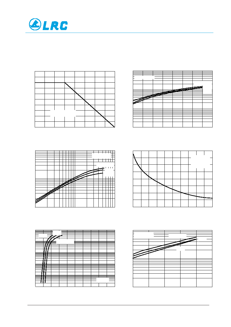
TYPICAL ELECTRICAL CHARACTERISTICS
LMUN2211LT1
100
10
1
0.1
0.01
0.001
0
1
2
3
4
Vin, INPUT VOLTAGE (VOLTS)
5
6
7
8
9
10
VO = 5 V
I C,
COLLECT
OR CURRENT (mA)
TA = ≠25
∞
C
75
∞
C
25
∞
C
1000
100
10
1
10
100
IC, COLLECTOR CURRENT (mA)
50
0
10
20
30
40
4
3
1
2
0
VR, REVERSE BIAS VOLTAGE (VOLTS)
f = 1 MHz
lE = 0 A
TA = 25
∞
C
VCE = 10 V
Figure 1. Derating Curve
250
200
150
100
50
0
≠50
0
50
100
150
TA, AMBIENT TEMPERATURE (5
∞
C)
Figure 2. VCE(sat) vs. IC
P
D,
POWER DISSIP
A
TION (MILLIW
A
TTS)
C
ob,
CAP
ACIT
ANCE (pF)
h
FE,
DC CURRENT GAIN (NORMALIZED)
R
JA= 625
∞
C/W
TA = 75
∞
C
≠25
∞
C
25
∞
C
10
0
20
30
IC, COLLECTOR CURRENT (mA)
10
1
0.1
40
50
Figure 3. DC Current Gain
V
in,
INPUT VOL
T
AGE (VOL
TS)
TA = ≠25
∞
C
75
∞
C
25
∞
C
VO = 0.2 V
1
0.1
0.01
0.001
0
20
40
60
80
IC, COLLECTOR CURRENT (mA)
IC/IB = 10
V
CE(sat),
MAXIMUM COLLECT
OR VOL
T
AGE
(VOL
TS)
TA = ≠25
∞
C
75
∞
C
25
∞
C
Figure 4. Output Capcitance
Figure 5. Output Current vs. Input Voltage
Figure 6. Input Voltage vs. Output Current

LESHAN RADIO COMPANY, LTD.
LMUN2211S≠5/11
LMUN2211LT1 Series
TYPICAL ELECTRICAL CHARACTERISTICS
LMUN2212LT1
Figure 7. VCE(sat) vs. IC
0.001
0.01
0.1
1
40
IC, COLLECTOR CURRENT (mA)
0
20
60
80
IC/IB = 10
≠
V
CE(sat),
MAXIMUM COLLECT
OR VOL
T
AGE
(VOL
TS)
TA = ≠25
∞
C
25
∞
C
75
∞
C
Figure 8. DC Current Gain
1000
10
IC, COLLECTOR CURRENT (mA
)
100
10
1
100
VCE = 10 V
h
FE,
DC CURRENT GAIN (NORMALIZED)
TA = 75
∞
C
25
∞
C
≠25
∞
C
C
ob,
CAP
ACIT
ANCE (pF)
Figure 9. Output Capacitance
Figure 10. Output Current vs. Input Voltage
100
0
Vin, INPUT VOLTAGE (VOLTS)
10
1
0.1
0.01
0.001
2
4
6
8
10
0
IC, COLLECTOR CURRENT (mA)
100
10
1
0.1
10
20
30
40
50
Figure 11. Input Voltage vs. Output Current
50
0
10
20
30
40
4
3
2
1
0
VR, REVERSE BIAS VOLTAGE (VOLTS)
f = 1 MHz
lE = 0 A
TA = 25
∞
C
VO = 5 V
VO = 0.2 V
I C,
COLLECT
OR CURRENT (mA)
V
in,
INPUT VOL
T
AGE (VOL
TS)
TA = ≠25
∞
C
75
∞
C
25
∞
C
TA = ≠25
∞
C
75
∞
C
25
∞
C