
�
8101/8104
Gigabit Ethernet
Controller
TECHNICAL
MANUAL
N o v e m b e r 2 0 0 1

ii
Copyright � 2000�2001 by LSI Logic Corporation. All rights reserved.
This document contains proprietary information of LSI Logic Corporation. The
information contained herein is not to be used by or disclosed to third parties
without the express written permission of an officer of LSI Logic Corporation.
Document DB14-000123-04, Fourth Edition (November 2001)
This document describes revision/release 1 of the LSI Logic Corporation
8101/8104 Gigabit Ethernet Controller and will remain the official reference
source for all revisions/releases of this product until rescinded by an update.
LSI Logic Corporation reserves the right to make changes to any products herein
at any time without notice. LSI Logic does not assume any responsibility or
liability arising out of the application or use of any product described herein,
except as expressly agreed to in writing by LSI Logic; nor does the purchase or
use of a product from LSI Logic convey a license under any patent rights,
copyrights, trademark rights, or any other of the intellectual property rights of
LSI Logic or third parties.
Copyright � 2000�2001 by LSI Logic Corporation. All rights reserved. Portions
TRADEMARK ACKNOWLEDGMENT
The LSI Logic logo design is a registered trademark of LSI Logic Corporation. All
other brand and product names may be trademarks of their respective
companies.
IF
To receive product literature, visit us at http://www.lsilogic.com.
For a current list of our distributors, sales offices, and design resource
centers, view our web page located at
http://www.lsilogic.com/contacts/na_salesoffices.html

8101/8104 Gigabit Ethernet Controller
iii
Copyright � 2000�2001 by LSI Logic Corporation. All rights reserved.
Preface
This book is the primary reference and technical manual for the
8101/8104 Gigabit Ethernet Controller. It contains a complete functional
description and includes complete physical and electrical specifications
for the 8101/8104.
The 8104 is functionally the same as the 8101, except that the 8104 is
in a 208-pin Ball Grid Array (BGA) package and the 8101 is in a 208-pin
Plastic Quad Flat Pack (PQFP) package
Audience
This document assumes that you have some familiarity with application
specific integrated circuits and related support devices. The people who
benefit from this book are:
�
Engineers and managers who are evaluating the 8101/8104 Gigabit
Ethernet Controller for possible use in a system
�
Engineers who are designing the 8101/8104 Gigabit Ethernet
Controller into a system
Organization
This document has the following chapters:
�
Chapter 1, Introduction
, describes the 8101/8104 Gigabit Ethernet
Controller, its basic features and benifits. This chapter also describes
the differences between the 8101 and 8104.
�
Chapter 2, Functional Description
, provides a high level
description of the 8101/8104 Gigabit Ethernet Controller.

iv
Preface
Copyright � 2000�2001 by LSI Logic Corporation. All rights reserved.
�
Chapter 3, Signal Descriptions
, provides a description of the
signals used and generated by the 8101/8104 Gigabit Ethernet
Controller.
�
Chapter 4, Registers
, provides a description of the register
addresses and definitions.
�
Chapter 5, Application Information
, provides application
considerations.
�
Chapter 6, Specifications
, describes the specifications of the
8101/8104 Gigabit Ethernet Controller.
Abbreviations Used in This Manual
100BASE-FX
100 Mbit/s Fiber Optic Ethernet
100BASE-TX
100 Mbit/s Twisted-Pair Ethernet
10BASE-T
10 Mbit/s Twisted-Pair Ethernet
4B5B
4-Bit 5-Bit
BGA
Ball Grid Array
CLK
Clock
CRC
Cyclic Redundancy Check
CRS
Carrier Sense
CSMA
Carrier Sense Multiple Access
CWRD
Codeword
DA
Destination Address
ECL
Emitter-Coupled Logic
EOF
End of Frame
ESD
End of Stream Delimiter
FCS
Frame Check Sequence
FDX
Full-Duplex
FEF
Far End Fault
FLP
Fast Link Pulse
FX
Fiber
HDX
Half-Duplex
HIZ
High Impedance
I/G
Individual/Group
IETF
Internet Engineering Task Force
IPG
Interpacket Gap
IREF
Reference Current
L/T
Length and Type
LSB
Least Significant Bit

Preface
v
Copyright � 2000�2001 by LSI Logic Corporation. All rights reserved.
MIB
Management Information Base
MLT3
Multilevel Transmission (3 levels)
MSB
Most Significant Bit
mV
millivolt
NLP
Normal Link Pulse
NRZI
Nonreturn to Zero Inverted
NRZ
Nonreturn to Zero
OP
Opcode
PCB
Printed Circuit Board
pF
picofarad
PRE
Preamble
R/LH
Read Latched High
R/LHI
Read Latched High with Interrupt
R/LL
Read Latched Low
R/LLI
Read Latched Low with Interrupt
R/LT
Read Latched Transition
R/LTI
Read Latched Transition with Interrupt
R/WSC
Read/Write Self Clearing
RFC
Request for Comments
RJ-45
Registered Jack-45
RMON
Remote Monitoring
SA
Start Address or Station Address
SFD
Start of Frame Delimiter
SNMP
Simple Network Management Protocol
SOI
Start of Idle
Split-32
Independent 32-bit input and output busses; one for
transmit and one for receive
SSD
Start of Stream Delimiter
STP
Shielded Twisted Pair
TP
Twisted Pair
�
H
microHenry
�
P
microprocessor
UTP
Unshielded Twisted Pair
Conventions Used in This Manual
The first time a word or phrase is defined in this manual, it is italicized.

vi
Preface
Copyright � 2000�2001 by LSI Logic Corporation. All rights reserved.
The word assert means to drive a signal true or active. The word
deassert means to drive a signal false or inactive. Signals that are active
LOW end in an "n."
Hexadecimal numbers are indicated by the prefix "0x" --for example,
0x32CF. Binary numbers are indicated by the prefix "0b" --for example,
0b0011.0010.1100.1111.

8101/8104 Gigabit Ethernet Controller
vii
Copyright � 2000�2001 by LSI Logic Corporation. All rights reserved.
Contents
CChapter 1
Introduction
1.1
Overview
1-1
1.2
Features
1-2
Chapter 2
Functional Description
2.1
Overview
2-2
2.2
Transmit Data Path
2-2
2.3
Receive Data Path
2-6
2.4
Register Structure
2-6
2.5
Ethernet Frame Format
2-6
2.5.1
Preamble and SFD
2-7
2.5.2
Destination Address
2-7
2.5.3
Source Address
2-7
2.5.4
Length/Type Field
2-7
2.5.5
Data
2-8
2.5.6
Frame Check Sequence (FCS)
2-8
2.5.7
Interpacket Gap (IPG)
2-8
2.6
System Interface
2-8
2.6.1
Data Format and Bit Order
2-8
2.6.2
Transmit Timing
2-9
2.6.3
Receive Timing
2-11
2.6.4
Bus Width
2-14
2.6.5
System Interface Disable
2-14
2.7
Transmit MAC
2-15
2.7.1
Preamble and SFD Generation
2-15
2.7.2
AutoPad
2-15
2.7.3
CRC Generation
2-15
2.7.4
Interpacket Gap
2-16
2.7.5
MAC Control Frame Generation
2-17

viii
Contents
Copyright � 2000�2001 by LSI Logic Corporation. All rights reserved.
2.8
Receive MAC
2-17
2.8.1
Preamble and SFD Stripping
2-17
2.8.2
CRC Stripping
2-17
2.8.3
Unicast Address Filter
2-18
2.8.4
Multicast Address Filter
2-18
2.8.5
Broadcast Address Filter
2-19
2.8.6
Reject or Accept All Packets
2-20
2.8.7
Frame Validity Checks
2-20
2.8.8
Maximum Packet Size
2-21
2.8.9
MAC Control Frame Check
2-21
2.9
Transmit FIFO
2-22
2.9.1
AutoSend
2-22
2.9.2
Watermarks
2-22
2.9.3
TX Underflow
2-23
2.9.4
TX Overflow
2-23
2.9.5
Link Down FIFO Flush
2-24
2.10
Receive FIFO
2-24
2.10.1
Watermarks
2-24
2.10.2
RX Overflow
2-25
2.10.3
RX Underflow
2-25
2.11
8B10B PCS
2-25
2.11.1
8B10B Encoder
2-26
2.11.2
8B10B Decoder
2-28
2.11.3
Start of Packet
2-29
2.11.4
End Of Packet
2-30
2.11.5
Idle
2-30
2.11.6
Receive Word Synchronization
2-31
2.11.7
AutoNegotiation
2-31
2.12
10-Bit PHY Interface
2-31
2.12.1
Data Format and Bit Order
2-32
2.12.2
Transmit
2-32
2.12.3
Receive
2-32
2.12.4
Lock To Reference
2-33
2.12.5
PHY Loopback
2-33
2.12.6
Signal Detect
2-33
2.12.7
TBC Disable
2-34
2.13
Packet Discard
2-34
2.13.1
Transmit Discards
2-34

Contents
ix
Copyright � 2000�2001 by LSI Logic Corporation. All rights reserved.
2.13.2
Receive Discards
2-35
2.13.3
Discard Output Indication
2-36
2.13.4
AutoClear Mode
2-36
2.13.5
AutoAbort Mode
2-36
2.14
Receive Status Word
2-37
2.14.1
Format
2-37
2.14.2
Append Options
2-38
2.14.3
Status Word for Discarded Packets
2-38
2.14.4
Status Word for RXABORT Packets
2-38
2.15
AutoNegotiation
2-39
2.15.1
Next Page
2-40
2.15.2
Negotiation Status
2-41
2.15.3
AutoNegotiation Restart
2-41
2.15.4
AutoNegotiation Enable
2-42
2.15.5
Link Indication
2-42
2.16
Flow Control
2-42
2.17
MAC Control Frames
2-42
2.17.1
Automatic Pause Frame Generation
2-43
2.17.2
Transmitter Pause Disable
2-44
2.17.3
Pass Through to FIFO
2-44
2.17.4
Reserved Multicast Address Disable
2-46
2.17.5
MAC Control Frame AutoSend
2-46
2.18
Reset
2-46
2.19
Counters
2-47
2.19.1
Counter Half Full
2-57
2.19.2
Counter Reset On Read
2-57
2.19.3
Counter Rollover
2-58
2.19.4
Counter Maximum Packet Size
2-58
2.19.5
Counter Reset
2-58
2.20
Loopback
2-59
2.21
Test Modes
2-59
Chapter 3
Signal Descriptions
3.1
System Interface Signals
3-3
3.2
10-Bit PHY Interface Signals
3-7
3.3
Register Interface Signals
3-8
3.4
Micellaneous Signals
3-9

x
Contents
Copyright � 2000�2001 by LSI Logic Corporation. All rights reserved.
3.5
Power Supply Signals
3-10
Chapter 4
Registers
4.1
Register Interface
4-1
4.1.1
Bit Types
4-2
4.1.2
Interrupt
4-3
4.1.3
Register Structure
4-4
4.2
Register Addresses
4-4
4.3
Register Definitions
4-11
4.3.1
Register 0�MAC Address 1
4-11
4.3.2
Register 1�MAC Address 2
4-12
4.3.3
Register 2�MAC Address 3
4-12
4.3.4
Register 3�MAC Address Filter 1
4-12
4.3.5
Register 4�MAC Address Filter 2
4-13
4.3.6
Register 5�MAC Address Filter 3
4-14
4.3.7
Register 6�MAC Address Filter 4
4-14
4.3.8
Register 7�Configuration 1
4-15
4.3.9
Register 8�Configuration 2
4-17
4.3.10
Register 9�Configuration 3
4-19
4.3.11
Register 10�Configuration 4
4-22
4.3.12
Register 11�Status 1
4-23
4.3.13
Register 14�Status Mask 1
4-25
4.3.14
Register 17�Transmit FIFO Threshold
4-26
4.3.15
Register 18�Receive FIFO Threshold
4-27
4.3.16
Register 19�Flow Control 1
4-28
4.3.17
Register 20�Flow Control 2
4-29
4.3.18
Register 21�AutoNegotiation Base Page
Transmit
4-30
4.3.19
Register 22�AutoNegotiation Base Page
Receive
4-31
4.3.20
Register 23�AutoNegotiation Next Page
Transmit
4-33
4.3.21
Register 24�AutoNegotiation Next Page
Receive
4-34
4.3.22
Register 32�Device ID
4-35
4.3.23
Register 112�115�Counter Half Full 1
-
4
4-36
4.3.24
Registers 120�123�Counter Half Full Mask 1
-
4
4-36
4.3.25
Registers 128
-
233�Counter 1
-
53
4-37

Contents
xi
Copyright � 2000�2001 by LSI Logic Corporation. All rights reserved.
Chapter 5
Application Information
5.1
Typical Ethernet Port
5-2
5.2
10-Bit PHY Interface
5-2
5.2.1
External Physical Layer Devices
5-2
5.2.2
Printed Circuit Board Layout
5-3
5.3
System Interface
5-3
5.3.1
Watermarks
5-3
5.3.2
PCB Layout
5-5
5.4
Reset
5-5
5.5
Loopback
5-6
5.6
AutoNegotiation
5-7
5.6.1
AutoNegotiation at Power Up
5-8
5.6.2
Negotiating with a Non-AutoNegotiation
Capable Device
5-9
5.7
Management Counters
5-9
5.8
TX Packet and Octet Counters
5-16
5.9
Power Supply Decoupling
5-16
Chapter 6
Specifications
6.1
Absolute Maximum Ratings
6-1
6.2
DC Electrical Characteristics
6-2
6.3
AC Electrical Characteristics
6-3
6.4
8101/8104 Pinouts and Pin Listings
6-17
6.5
Package Mechanical Dimensions
6-21
Customer Feedback

xii
Contents
Copyright � 2000�2001 by LSI Logic Corporation. All rights reserved.

xiii
Copyright � 2000�2001 by LSI Logic Corporation. All rights reserved.
Figures
2.1
8101/8104 Block Diagram
2-3
2.2
Ethernet MAC Frame Format
2-4
2.3
Frame Formats and Bit Ordering
2-5
2.4
Little Endian vs. Big Endian Format
2-9
2.5
RXSOF/RXEOF Position
2-13
2.6
AutoNegotiation Data Format
2-39
2.7
Autogenerated Pause Frame Format
2-45
3.1
8101/8104 Interface Diagram
3-2
5.1
Gigabit Ethernet Switch Port Using the 8101/8104
5-2
5.2
Decoupling Recommendations
5-17
6.1
Input Clock Timing
6-4
6.2
Transmit System Interface Timing
6-6
6.3
Receive System Interface Timing
6-8
6.4
Receive System Interface RXABORT Timing
6-9
6.5
Receive System Interface RXOEn Timing
6-9
6.6
System Interface RXDC/TXDC Timing
6-10
6.7
Transmit 10-Bit PHY Interface Timing
6-11
6.8
Receive 10-Bit PHY Interface Timing
6-12
6.9
Register Interface Timing (Excluding Counter
Read Cycle)
6-14
6.10
Register Interface Timing, Counter Read Cycle
(of the Same Counter)
6-15
6.11
Register Interface Timing, Counter Read Cycle
(Between Different Counters)
6-16
6.12
8101 208-Pin PQFP Pinout
6-17
6.13
8104 208-Pin BGA Pinout
6-19
6.14
208-Pin PQFP Mechanical Drawing
6-21
6.15
208 mini-BGA (HG) Mechanical Drawing
6-22

xiv
Copyright � 2000�2001 by LSI Logic Corporation. All rights reserved.

xv
Copyright � 2000�2001 by LSI Logic Corporation. All rights reserved.
Tables
2.1
Length/Type Field Definition
2-8
2.2
Byte Enable Pin vs. Valid Byte Position
2-10
2.3
TXRC Bit and TXCRCn Pin Logic
2-16
2.4
Transmit IPG Selection
2-16
2.5
Multicast Address Filter Map
2-19
2.6
Receive Maximum Packet Size Selection
2-21
2.7
8B10B Coding Table
2-27
2.8
10B Defined Ordered Sets
2-28
2.9
Transmit Discard Conditions
2-34
2.10
Receive Discard Conditions
2-35
2.11
Receive Status Word Definition
2-37
2.12
AutoNegotiation Status Bits
2-41
2.13
Reset Description
2-47
2.14
Counter Definition
2-49
2.15
Counter Maximum Packet Size Selection
2-58
4.1
Register Bit Type Definition
4-3
4.2
Register Addresses
4-4
4.3
Register Default Values
4-10
5.1
Compatible SerDes Devices
5-3
5.2
Reset Procedure
5-6
5.3
SerDes Loopback Procedure
5-7
5.4
AutoNegotiation Power Up Procedure
5-8
5.5
MIB Objects vs. Counter Location for RMON
Statistics Group MIB (RFC 1757)
5-10
5.6
MIB Objects vs. Counter Location for SNMP
Interface Group MIB (RFC 1213 and 1573)
5-11
5.7
MIB Objects vs. Counter Location for Ethernet-Like
Group MIB (RFC 1643)
5-13
5.8
MIB Objects vs. Counter Location For Ethernet MIB
(IEEE 802.3z, Clause 30)
5-14
6.1
DC Electrical Characteristics
6-2
6.2
Input Clock Timing Characteristics
6-4
6.3
Transmit System Interface Timing Characteristics
6-5
6.4
Receive System Interface Timing Characteristics
6-7
6.5
System Interface RXDC/TXDC Timing Characteristics
6-10
6.6
Transmit 10-Bit PHY Interface Timing Characteristics
6-11

xvi
Copyright � 2000�2001 by LSI Logic Corporation. All rights reserved.
6.7
Receive 10-Bit PHY Interface Timing Characteristics
6-12
6.8
Register Interface Timing Characteristics
6-13
6.9
8101 208-Pin PQFP Pin List (Alphabetical Listing)
6-18
6.10
8104 208-Pin BGA Pin List (Alphabetical Listing)
6-21

8101/8104 Gigabit Ethernet Controller
1-1
Copyright � 2000�2001 by LSI Logic Corporation. All rights reserved.
Chapter 1
Introduction
This chapter contains a brief introduction to the 8101/8104 Gigabit
Ethernet Controller. It consists of the following sections:
�
Section 1.1, "Overview"
�
Section 1.2, "Features"
1.1 Overview
The 8101/8104 Gigabit Ethernet Controller is a complete media access
controller (MAC sublayer) with integrated coding logic for fiber and short
haul copper media (8 bit/10 bit Physical Coding Sublayer) (8B10B PCS)
for 1000 Mbits/s Gigabit Ethernet systems.
The 8104 is functionally the same as the 8101 except that the 8104 is in
a 208-pin Ball Grid Array (BGA) package and the 8101 is in a 208-pin
Plastic Quad Flat Pack (PQFP) package
The Controller consists of a 32-bit system interface, receive/transmit First
In, First Out (FIFO) buffers, a full-duplex Ethernet Media Access
Controller (MAC), an 8 bit/10 bit PCS, a 10-bit Physical Layer Device
(PHY) interface, and a 16-bit register interface. The controller also
contains all the necessary circuitry to implement the IEEE 802.3x Flow
Control Algorithm. Flow control messages can be sent automatically
without host intervention.
The controller contains 53 counters which satisfy the management
objectives of the Remote Monitoring (RMON) Statistics Group MIB,
(RFC 1757), Simple Network Management Protocol (SNMP) Interfaces
Group (RFC 1213 and 1573), Ethernet-Like Group MIB (RFC 1643), and
Ethernet MIB (IEEE 802.3z Clause 30). The controller also contains 136

1-2
Introduction
Copyright � 2000�2001 by LSI Logic Corporation. All rights reserved.
internal 16-bit registers that can be accessed through the register
interface. These registers contain configuration inputs, status outputs,
and management counter results.
The 8101/8104 is ideal as an Ethernet controller for Gigabit Ethernet
switch ports, uplinks, backbones, and adapter cards.
1.2 Features
The 8101/8104 provides the following features.
�
Pin-compatible upgrade of 8100
�
Combined Ethernet MAC and 8B10B PCS
�
1000 Mbits/s data rate
�
64-bit, 66 MHz external bus interface (4 Gbits/s bandwidth)
�
10-bit interface to external SerDes chip
�
16-bit interface to internal registers and management counters
�
Full RMON, SNMP, and Ethernet management counter support
�
Independent receive and transmit FIFOs with programmable
watermarks
�
16 Kbytes receive FIFO size
�
4 Kbytes transmit FIFO size
�
AutoNegotiation algorithm on chip
�
Full duplex only
�
Flow control per IEEE 802.3x
�
Automatic CRC generation and checking
�
Automatic packet error discarding
�
Programmable transmit start threshold
�
Interrupt capability
�
Support for fiber and short haul copper media
�
3.3 V power supply, 5 V tolerant inputs
�
IEEE 802.3 and 802.3z specification compliant

8101/8104 Gigabit Ethernet Controller
2-1
Copyright � 2000�2001 by LSI Logic Corporation. All rights reserved.
Chapter 2
Functional Description
This chapter provides a high level description of the 8101/8104 Gigabit
Ethernet Controller and consists of the following sections:
�
Section 2.1, "Overview"
�
Section 2.2, "Transmit Data Path"
�
Section 2.3, "Receive Data Path"
�
Section 2.4, "Register Structure"
�
Section 2.5, "Ethernet Frame Format"
�
Section 2.6, "System Interface"
�
Section 2.7, "Transmit MAC"
�
Section 2.8, "Receive MAC"
�
Section 2.9, "Transmit FIFO"
�
Section 2.10, "Receive FIFO"
�
Section 2.11, "8B10B PCS"
�
Section 2.12, "10-Bit PHY Interface"
�
Section 2.13, "Packet Discard"
�
Section 2.14, "Receive Status Word"
�
Section 2.15, "AutoNegotiation"
�
Section 2.16, "Flow Control"
�
Section 2.17, "MAC Control Frames"
�
Section 2.18, "Reset"
�
Section 2.19, "Counters"
�
Section 2.20, "Loopback"
�
Section 2.21, "Test Modes"

2-2
Functional Description
Copyright � 2000�2001 by LSI Logic Corporation. All rights reserved.
2.1 Overview
The 8101/8104 is a complete Media Access Controller (MAC) sublayer
with integrated coding logic for fiber and short haul copper media (8B10B
PCS sublayer) for 1000 Mbits/s Gigabit Ethernet systems. The controller
has seven main sections:
�
System interface
�
FIFOs
�
MAC
�
8B10B PCS
�
10-bit PHY interface
�
Register interface.
�
Management counters
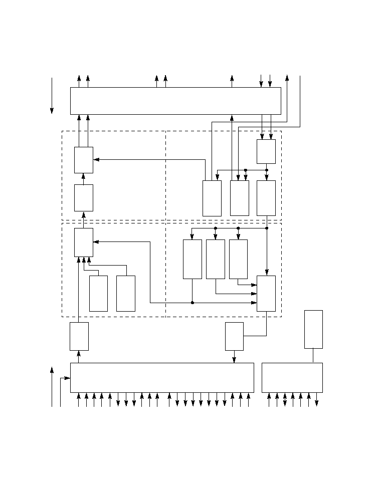
A block diagram is shown in
Figure 2.1
.
The controller has a transmit data path and a receive data path. The
transmit data path goes in the system interface and out the 10-bit PHY
interface, as shown in the top half of
Figure 2.1
. The receive data path
goes in the 10-bit PHY interface and out the system interface, as shown
in the bottom half of
Figure 2.1
.
2.2 Transmit Data Path
Data is input to the system from an external bus. The data is then sent
to the transmit FIFO. The transmit FIFO provides temporary storage of
the data until it is sent to the MAC transmit section. The transmit MAC
formats the data into an Ethernet packet according to IEEE 802.3
specification as shown in
Figure 2.2
. The transmit MAC also generates
MAC control frames and includes logic for AutoNegotiation. The Ethernet
frame packet is then sent to the 8B10B PCS.
The 8B10B PCS encodes the data and adds appropriate framing
delimiters to create 10-bit symbols as specified in IEEE 802.3 and shown
in
Figure 2.3
. The 10-bit symbols are then sent to the 10-bit PHY
interface for transmission to an external PHY device.
2-3
Functional
Descr
iption
Cop
yr
ight
�
2000�2001
b
y
LSI
Logic
Cor
por
ation.
All
r
ights
reser
v
ed.
Figure 2.1
8101/8104 Block Diagram
REGCSn
RESETn
SCLK
TXENn
TXD[31:0]
TXBE[3:0]
TXSOF
TXEOF
TXWM1n
TXWM2n
TXDC
CLR_TXDC
TXCRCn
RXENn
RXD[31:0]
RXBE[3:0]
RXSOF
RXEOF
RXWM1
RXWM2
RXDC
CLR_RXDC
RXABORT
RXOEn
REGCLK
REGD[15:0]
REGAD[7:0]
REGRDn
REGWRn
REGINT
System
Interface
Register
Interface
&
Registers
Transmit
FIFO
Packet
Generator
Receive
FIFO
Management
Counters
CRC
Generator
MAC Control
Frame Gen.
MAC
8B10B
Encoder
Transmit
8B10B PCS
Packet
Decompose
MAC Control
Frame Check
Address
Filter
CRC
Check
Receive
Transmit
Receive
Transmit
8B10B
Decoder
Link
Configuration
Receive
Receive
Sync.
TCLK
10-Bit
PHY
Interface
TX[9:0]
TBC
EWRAP
EN_CDET
LCK_REFn
SD
LINKn
RX[0:9]
RBC[1:0]
FCNTRL

2-4
Functional Description
Copyright � 2000�2001 by LSI Logic Corporation. All rights reserved.
Figure 2.2
Ethernet MAC Frame Format
Preamble
Start of Frame
Delimiter (SFD)
Destination
Address (DA)
Source
Address (SA)
Length/Type (L/T)
Data
Frame Check
Sequence (FCS)
7 Bytes
1 Byte
6 Bytes
6 Bytes
2 Bytes
46�1500 Bytes
4 Bytes
See
Below
Bytes Within
Frame Transmitted
Top to Bottom
A0
LSB
A7
MSB
Bits Within
Frame Transmitted
Left to Right
a. Frame Format
b. Address Field Format
I/G U/L 40-Bit Address
A0
A47
1 = Broadcast
0 = Multicast
1 = Multicast or Broadcast
0 = Unicast
Bits in
Registers 0�2

Transmit Data Path
2-5
Copyright � 2000�2001 by LSI Logic Corporation. All rights reserved.
Figure 2.3
Frame Formats and Bit Ordering
MAC
10-Bit PHY
10101010
10101010
10101010
10101010
10101010
10101010
10101010
10101011
DA [0:7]
DATA[0:7]
[5] PRE
SFD
DA
SA
L/T
DATA
[6] FCS
Notes:
[1]
Status word on receive only is
programmable
[2]
EOF position is programmable
[3]
Little endian format (default)
[4]
Second /R/ added only if transmit packet
ends on odd number of bytes
[5]
XMT preamble appended
Receive preamble stripped
[6]
XMT CRC not appended
Receive CRC not stripped
[7]
< > Means 10B encoded
[8]
/I1/ or /I2/, depends on running disparity
System Interface
DA [8:15]
DA [16:23]
DA [24:31]
DA [32:39]
DA [40:47]
SA [0:7]
SA [8:15]
SA [16:23]
SA [24:31]
SA [32:39]
SA [40:47]
LT [0:7]
LT [8:15]
DATA[8:15]
DATA[16:23]
DATA[24:31]
FCS[31:24]
FCS[23:16]
FCS[15:8]
FCS[7:0]
Interface
/I2/
/I2/
/S/
D21.2
D21.2
D21.2
D21.2
D21.2
D21.2
D21.6
[7]
<DA [0:7]>
<DA [8:15]>
<DA [16:23]>
<DA [24:31]>
<DA [32:39]>
<DA [40:47]>
<SA [0:7]>
<SA [8:15]>
<SA [16:23]>
<SA [24:31]>
<SA [32:39]>
<SA [40:47]>
<DATA[0:7]>
<LT [0:7]>
<LT [8:15]>
<DATA[8:15]>
<DATA[16:23]>
<DATA[24:31]>
<FCS[31:24]>
<FCS[23:16]>
<FCS[15:8]>
<FCS[7:0]>
/R/
/T/
/R/
/I1/ or /I2/
/I2/
/I2/
A B C D E F G H
a b c d e f g h i j
[4]
[8]
DA[0:7]
DA[32:39]
SA[16:23]
LT[0:7]
DATA[16:23]
DA[8:15]
DA[40:47]
SA[24:31]
LT[8:16]
DATA[24:31]
SOF
DA[16:23]
SA[0:7]
SA[32:39]
DATA[0:7]
DA[24:31]
SA[8:15]
SA[40:47]
DATA[7:15]
FCS[15:8]
FCS[7:0]
FCS[31:24]
FCS[23:16]
STATUS WORD [1]
INVALID
EOF
TXD[0]
[2]
RXD[0]
TXD[31]
RXD[31]
[3]
MSB
MSB
LSB
TX[0]
RX[0]
TX[9]
RX[9]
10-Bit
PHY
Interface
PCS 10B
PCS 8B
Bits
Transmitted
Bytes
Transmitted
LSB

2-6
Functional Description
Copyright � 2000�2001 by LSI Logic Corporation. All rights reserved.
2.3 Receive Data Path
The 10-bit PHY interface receives incoming encoded data from an
external PHY device. The incoming encoded data must be encoded in
the 10-bit PHY format specified in IEEE 802.3z, as shown in
Figure 2.3
.
The incoming encoded data is then sent to the receive 8B10B PCS
block, which strips off the framing delimiters, decodes the data, and
converts the encoded data into an Ethernet packet according to the
IEEE 802.3 specifications, as shown in
Figure 2.2
. The Ethernet packet
data is then sent to the receive MAC section.
The receive MAC section disassembles the packet, checks the validity of
the packet against certain error criteria and address filters, and checks
for MAC control frames. The receive MAC then sends valid packets to
the receive FIFO. The receive FIFO provides temporary storage of data
until it is demanded by the system interface. The system interface
outputs the data to an external bus.
2.4 Register Structure
The controller has 136 internal 16-bit registers. 22 registers are available
for setting configuration inputs and reading status outputs. The remaining
114 registers are associated with the management counters.
The register interface is a separate internal register bidirectional 16 bit
data bus to set configuration inputs, read status outputs, and access
management counters.
The location of all registers is described in the Register Addressing Table
in
Section 4.2, "Register Addresses"
. The description of each bit for each
register is described in Section
4.3.1
through Section
4.3.25
.
2.5 Ethernet Frame Format
Information in an Ethernet network is transmitted and received in packets
or frames. The basic function of the controller is to process Ethernet
frames. An Ethernet frame is defined in IEEE 802.3 and consists of a
preamble, start of frame delimiter (SFD), destination address (DA),

Ethernet Frame Format
2-7
Copyright � 2000�2001 by LSI Logic Corporation. All rights reserved.
source address (SA), length/type field (L/T), data, frame check sequence
(FCS), and interpacket gap (IPG). The format for the Ethernet frame is
shown in
Figure 2.2
.
An Ethernet frame is specified by IEEE 802.3 to have a minimum length
of 64 bytes and a maximum length of 1518 bytes, exclusive of the
preamble and SFD. Packets that are less than 64 bytes or greater than
1518 bytes are referred to as undersize and oversize packets,
respectively.
2.5.1 Preamble and SFD
The preamble and SFD is a combined 64-bit field consisting of 62
alternating ones and zeros followed by a 0b11 end of preamble indicator.
The first 56-bits of ones and zeros are considered to be the preamble,
and the last 8 bits (0b10101011) are considered to be the SFD.
2.5.2 Destination Address
The destination address is a 48-bit field containing the address of the
station(s) to which the frame is directed. The format of the address field
is the same as defined in IEEE 802.3 and shown in
Figure 2.2
b. The
destination address can be either a unicast address to a specific station,
a multicast address to a group of stations, or a broadcast address to all
stations. The first and second bits determine whether an address is
unicast, multicast or broadcast, and the remaining 46 bits are the actual
address bits, as shown in
Figure 2.2
b.
2.5.3 Source Address
The source address is a 48-bit field containing the specific station
address from which the frame originated. The format of the address field
is the same as defined in IEEE 802.3 and shown in
Figure 2.2
b.
2.5.4 Length/Type Field
The 16-bit length/type field takes on the meaning of either packet length
or packet type, depending on its numeric value, as described in
Table 2.1
.

2-8
Functional Description
Copyright � 2000�2001 by LSI Logic Corporation. All rights reserved.
2.5.5 Data
The data is a 46�1500 byte field containing the actual data to be
transmitted between two stations. If the actual data is less than 46 bytes,
extra zeros are added to increase the data field to the 46 byte minimum
size. Adding these extra zeros is referred to as padding.
2.5.6 Frame Check Sequence (FCS)
The FCS is a 32-bit cyclic redundancy check (CRC) value computed on
the entire frame, exclusive of preamble and SFD. The FCS algorithm is
defined in IEEE 802.3. The FCS is appended to the end of the frame and
determines frame validity.
2.5.7 Interpacket Gap (IPG)
The IPG is the time interval between packets. The minimum IPG value
is 96 bits, where 1 bit = 1 ns for Gigabit Ethernet. There is no maximum
IPG limit.
2.6 System Interface
The system interface is a 64-bit wide data interface consisting of
separate 32-bit data busses for transmit and receive.
2.6.1 Data Format and Bit Order
The format of the data word on TXD[31:0] and RXD[31:0] and its
relationship to the MAC frame format and 10-bit PHY interface format is
Table 2.1
Length/Type Field Definition
Length/Type
Field Value
(Decimal)
Length
or Type
Definition
0
-
1500
Length
Total number of bytes in data field
minus any padding
1501
-
1517
Neither
Undefined
1518
Type
Frame type
System Interface
2-9
Copyright � 2000�2001 by LSI Logic Corporation. All rights reserved.
shown in
Figure 2.3
. Note that the controller can be programmed to
append an additional 32-bit status word to the end of the receive packet.
Refer to
Section 2.14, "Receive Status Word,"
for more details on this
status word.
To program the byte ordering of the TXD and RXD data bits, set the
endian bit in
"Register 10�Configuration 4," Section 4.3.11
. The byte
order shown in
Figure 2.4
is with the little endian format mode (default).
If the controller is placed in big endian format, the byte order shown in
Figure 2.4
is reversed, DA[0:7] occurs on pins RXD[24:31], DA[24:31]
occurs on pins RXD[0:7]and so on. The endian bit affects all bytes in the
frame including the receive status word (if appended). The difference
between little endian and big endian format is illustrated in
Figure 2.4
.
Figure 2.4
Little Endian vs. Big Endian Format
2.6.2 Transmit Timing
The transmit portion of the system interface consists of 45 signals:
32 transmit data input bits (TXD[31:0]), one transmit enable (TXENn),
four transmit byte enable inputs (TXBE[3:0]), two transmit start of frame
and end of frame inputs (TXSOF and TXEOF), two transmit FIFO
watermark outputs (TXWM1n and TXWM2n), one transmit discard output
(TXDC), one transmit discard clear input (CLR_TXDC), one transmit
CRC enable input (TXCRCn), and one flow control enable input
(FCNTRL). All receive and transmit data is clocked in and out on the
rising edge of the system clock, SCLK. SCLK must operate between
33�66 MHz.
The SCLK input needs to be continuously input to the controller at
33�66 MHz. When TXENn is deasserted, the transmit interface is not
selected and subsequently, the controller accepts no input data from the
Little
Endian
(Default)
Preamble
DA0 . .. . . DA7
DA8 . . . . DA15
DA16 . . . DA23
DA40 . . . DA47
DA24 . . . DA31
DA32 . . . DA39
Source Address
Big
Endian
TXD[24] . . . TXD[31]
RXD[0] . . . RXD[7]
TXD[0] . . . TXD[7]
RXD[24] . . . RXD[31]
RXD[8] . . . RXD[15]
TXD[8] . . . TXD[15]
TXD[16]. . . TXD[23]
RXD[16] . . . RXD[23]
TXD[8] . . . TXD[15]
RXD[16] . . . RXD[23]
TXD[16] . . . TXD[23]
RXD[8] . . . RXD[15]
RXD[2]4 . . . RXD[31]
TXD[24] . . . TXD[31]
TXD[0] . . . TXD[7]
RXD[0] . . . RXD[7]
TXD[24] . . . TXD[31]
RXD[0] . . . RXD[7]
TXD[0] . . . TXD[7]
RXD[24] . . . RXD[31]
RXD[8] . . . RXD[15]
TXD[8] . . . TXD[15]
TXD[16] . . . TXD[23]
RXD[16] . . . RXD[23]
TXD[15] . . .
RXD[15]] . . .
TXD[16] . . .
RXD[16] . . .

2-10
Functional Description
Copyright � 2000�2001 by LSI Logic Corporation. All rights reserved.
transmit system interface inputs. When TXENn is asserted, a data word
on the TXD[31:0] input is clocked into the transmit FIFO on each rising
edge of the SCLK clock input. Multiple packets may be clocked in on one
TXENn assertion. The TXD[31:0] input data is a 32-bit wide packet data
whose format and relationship to the MAC packet and 10-bit PHY data
is described in
Figure 2.3
.
The TXBE[3:0] pins determine which bytes of the 32-bit TXD[31:0] data
word contain valid data. TXBE[3:0] are clocked in on the rising edge of
SCLK along with each TXD[31:0] data word. The correspondence
between the byte enable inputs and the valid bytes of each data word on
TXD[31:0] is defined in
Table 2.2
. Any logic combination of TXBE[3:0]
inputs is allowed, with the one exception that TXBE[3:0] must not be
0b0000 on the SCLK cycle when TXSOF or TXEOF is asserted.
The TXSOF and TXEOF signals indicate to the controller which data
words start and end the Ethernet data packet, respectively. These
signals are input on the same SCLK rising edge as the first and last word
of the data packet.
The TXWM1n and TXWM2n signals indicate when the transmit FIFO has
exceeded the programmable watermark thresholds. The controller
asserts the watermarks on the rising edge of SCLK, depending on the
fullness of the transmit FIFO. Refer to
Section 2.9, "Transmit FIFO,"
for
more details on these watermarks.
Table 2.2
Byte Enable Pin vs. Valid Byte Position
TXBE[3:0]/RXBE[3:0] Byte
Enable Pins
Valid Bytes on
TXD[31:0]/RXD[31:0] Pins
TXBE[3]/RXBE[3] Asserted
TXD[31:24]/RXD[31:24]
TXBE[2]/RXBE[2] Asserted
TXD[23:16]/RXD[23:16]
TXBE[1]/RXBE[1] Asserted
TXD[15:8]/RXD[15:8]
TXBE[0]/RXBE[0] Asserted
TXD[7:0]/RXD[7:0]

System Interface
2-11
Copyright � 2000�2001 by LSI Logic Corporation. All rights reserved.
TXDC is a transmit packet discard output. TXDC is asserted every time
the transmission of the packet being input on the system interface was
halted and the packet discarded due to some error. This signal is latched
HIGH. It is cleared when the clearing signal, CLR_TXDC, is asserted or
cleared automatically if the controller is placed in the AutoClear mode.
See
Section 2.13, "Packet Discard,"
for more details on discards and
TXDC.
TXCRCn is an input that can enable the internal generation and
appending of the 4-byte CRC value onto the end of the data packet.
TXCRCn is sampled on the rising edge of SCLK and has to be asserted
at the beginning of the packet, coincident with TXSOF, to remove or add
the CRC to that packet. Setting the transmit CRC enable bit (TXCRC) in
the Configuration 1 register also enables CRC generation. Refer to
Section 2.7.3, "CRC Generation"
for more details on CRC generation and
the interaction between TXCRCn and the TXCRC bit.
FCNTRL is an input that causes the automatic generation and
transmission of a MAC control pause frame. FCNTRL is input on the
rising edge of SCLK. See
Section 2.17, "MAC Control Frames,"
for more
details about this feature.
2.6.3 Receive Timing
The receive portion of the system interface consists of 45 signals:
�
32 receive output data bits (RXD[31:0])
�
One receive enable input (RXENn)
�
Four receive byte enable outputs (RXBE[3:0])
�
One receive start of frame and one end of frame outputs (RXSOF
and RXEOF)
�
Two receive FIFO watermark outputs (RXWM1 and RXWM2)
�
One receive discard output (RXDC)
�
One receive discard clear input (CLR_RXDC)
�
One receive packet abort input (RXABORT)
�
One receive output enable (RXOEn)
All receive and transmit data is clocked in and out with the system clock,
SCLK, which must operate between 33�66 MHz.

2-12
Functional Description
Copyright � 2000�2001 by LSI Logic Corporation. All rights reserved.
The SCLK input must continuously operate at 33�66 MHz. When RXENn
is deasserted, the receive interface is not selected and, subsequently, no
data from the receive FIFO can be output over the system interface. If
the receive watermarks RXWM1 and RXWM2 are asserted while RXENn
is deasserted, the next data word from the receive FIFO appears on the
RXD[31:0] outputs until RXENn is asserted. When RXENn is asserted,
a data word from the receive FIFO is clocked out onto the RXD[31:0]
outputs after each rising edge of the SCLK input. After the entire packet
has been clocked out, no more data is clocked out on RXD[31:0] until
RXENn is deasserted and reasserted, which allows extra dribble SCLK
clock cycles to occur after the end of the packet. RXD[31:0] output data
is a 32-bit wide packet data whose format and relationship to the MAC
packet and 10-bit PHY data is described in
Figure 2.3
.
The RXBE[3:0] signals determine which bytes of the 32-bit RXD[31:0]
data word contain valid data. RXBE[3:0] are clocked out on the rising
edge of SCLK along with each RXD[31:0] data word. Note that
RXBE[3:0] = 0b1111 for all words of the packet except the last word,
which may end on any one of the 4-byte boundaries of the 32-bit data
word. The correspondence between the byte enable inputs and the valid
data bytes of each data word on RXD[31:0] is defined in
Table 2.2
.
The RXSOF and RXEOF signals indicate which words start and end the
Ethernet data packet, respectively. These signals are generally clocked
out on the same SCLK rising edge as the first and last word of the data
packet, respectively. However, their exact position relative to the data
packet is dependent on the programming of the PEOF bit and
STSWRD[1:0] bits in Register 7, "Configuration 1". The exact RXSOF
and RXEOF position for combinations of these two bits is shown in
Figure 2.5
. More details about the definition of these bits can be found
in
"Register 7�Configuration 1," Section 4.3.8
, and more details about the
status word can be found in
Section 2.14, "Receive Status Word,"
.

System Interface
2-13
Copyright � 2000�2001 by LSI Logic Corporation. All rights reserved.
Figure 2.5
RXSOF/RXEOF Position
The RXWM1 and RXWM2 signals indicate when the receive FIFO has
exceeded the programmable watermark thresholds. The watermarks are
asserted or deasserted on the rising edge of SCLK, depending on the
fullness of the receive FIFO. Refer to
Section 2.10, "Receive FIFO,"
for
more details on these watermarks.
RXDC is asserted every time a received packet being output over the
system interface is halted and the packet discarded due to some error.
This signal is latched HIGH and can be cleared by either asserting the
clearing signal, CLR_RXDC, or cleared automatically if the controller is
placed in the AutoClear mode. See
Section 2.13, "Packet Discard,"
section for more details on discards and RXDC.
The RXABORT input, when asserted, discards the current packet being
output on the system interface. When RXABORT is asserted, a packet
is discarded and the remaining contents of that packet in the receive
FIFO are flushed. The process of flushing a receive packet from the
receive FIFO with the RXABORT pin requires extra SCLK cycles equal
to (packet length in bytes)/8 + 6. Refer to
Section 2.13, "Packet Discard,"
for more information about discarded packets. Clearing the discard
RXABORT enable bit in
"Register 8�Configuration 2," Section 4.3.9
,
programs the controller to ignore the RXABORT signal. Setting the
First Data Word
Discard Status Word
Status Word
Last Data Word
Packet
Data
RX FIFO Data
00X
SOF
010
SOF
011
SOF
100
SOF
101
SOF
11X
[1]
[1]
EOF
[1]
[1]
EOF
SOF, EOF
SOF, EOF
EOF
EOF
EOF
R
e
s
e
r
v
e
d
Note:
[1] Status words do not exist with this bit combination
Bits 7.2 � 7.0 (STSWRD [1:0], PEOF)
RXSOF/RXEOF Position

2-14
Functional Description
Copyright � 2000�2001 by LSI Logic Corporation. All rights reserved.
RXABORT definition bit in
"Register 9�Configuration 3," Section 4.3.10
,
also programs the controller to discard either the data packet and its
status word or just the data packet exclusive of the status word.
The RXOEn signal, when asserted, places certain receive outputs in the
high-impedance state. RXOEn affects the RXD[31:0], RXBE[3:0],
RXSOF, and RXEOF output pins.
2.6.4 Bus Width
Setting the BUSSIZE bit in
"Register 10�Configuration 4," Section 4.3.11
,
changes the receive word width from 32-bits to 16-bits. When the bus
width is configured to 16-bits, the receive system interface data outputs
appear on RXD[15:0] and the data words are now 16-bits wide instead
of 32-bits wide.
Note:
The transmit word width can be adjusted by appropriately
setting the transmit byte enable inputs, TXBE[3:0], as
described in
Table 2.2
.
2.6.5 System Interface Disable
To disable the system interface, set the SINTF_DIS bit in
"Register 9�
Configuration 3," Section 4.3.10
. When the system interface is disabled,
the controller:
�
Places all system interface outputs in the high-impedance state
(TXWMn[1:2], TXDC, RXD[31:0], RXBE[3:0], RXSOF, RXEOF,
RXWM1/2, RXDC)
�
Ignores all inputs (SCLK, TXENn, TXD[31:0], TXBE[3:0], TXSOF,
TXEOF, CLR_TXDC, FCNTRL, TXCRCn, RXENn, RXOEn,
CLR_RXDC, RXABORT)
�
Transmits /C/ (see
Table 2.8
) ordered sets with the remote fault bits
RF[1:0] = 0b10 over the 10-bit PHY interface outputs

Transmit MAC
2-15
Copyright � 2000�2001 by LSI Logic Corporation. All rights reserved.
2.7 Transmit MAC
To generate an Ethernet MAC frame from the transmit FIFO, the transmit
MAC section:
�
Generates preamble and SFD
�
Pads undersize packets with zeros to meet minimum packet size
requirements
�
Calculates and appends a CRC value to the packet
�
Maintains a minimum interpacket gap
Each of the above four operations can be individually disabled and
altered if desired. The transmit MAC then sends the fully formed Ethernet
packet to the 8B10B PCS block for encoding. The transmit MAC section
also generates MAC control frames.
2.7.1 Preamble and SFD Generation
The transmit MAC normally appends the preamble and SFD to the
packet. To program the controller to not append the preamble and SFD
to the transmit packet, clear the TXPRMBL bit in
"Register 7�
Configuration 1," Section 4.3.8
.
2.7.2 AutoPad
The transmit MAC normally AutoPads packets. AutoPadding is the
process of automatically adding enough zeroes in packets with data
fields less than 46 bytes to make the data field exactly 46 bytes in length
which meets the 46-byte minimum data field requirement of IEEE 802.3.
To program the controller to not AutoPad, clear the APAD bit in
"Register 7�Configuration 1," Section 4.3.8
.
2.7.3 CRC Generation
The transmit MAC normally appends the CRC value to the packet. To
program the controller to not append the CRC value to the end of the
packet from the transmit FIFO, assert the TXCRCn pin or clear the
TXCRC bit in Register 7 "Configuration 1", as described in
Table 2.3
and
as described in
"Register 7�Configuration 1," Section 4.3.8
.

2-16
Functional Description
Copyright � 2000�2001 by LSI Logic Corporation. All rights reserved.
1. 1 = Append, 0 = No append
2. 1 = No append, 0 = Append
2.7.4 Interpacket Gap
If packets from the transmit FIFO arrive at the transmit MAC sooner than
the minimum IPG time the transmit MAC adds enough time between
packets to equal the minimum IPG value. The default IPG time is set to
96 bits (1 bit = 1 ns).To program other values, set the transmit IPG select
bits IPG[2:0] in
"Register 7�Configuration 1," Section 4.3.8
, as
summarized in
Table 2.4
.
Table 2.3
TXRC Bit and TXCRCn Pin Logic
TXCRC Bit
1
TXCRCn
2
Pin
CRC Appended to End of Packet?
1
1
Yes
1
0
Yes
0
1
No
0
0
Yes
Table 2.4
Transmit IPG Selection
IPG[2:0]
Bits
IPG Value
(ns)
Comments
111
96
IEEE minimum specification
110
112
101
80
100
64
011
192
2
�
IEEE minimum specification
010
384
4
�
IEEE minimum specification
001
768
8
�
IEEE minimum specification
000
32

Receive MAC
2-17
Copyright � 2000�2001 by LSI Logic Corporation. All rights reserved.
2.7.5 MAC Control Frame Generation
The transmit MAC can automatically generate and transmit MAC control
pause frames, which are used for flow control. This function is described
in more detail in
Section 2.17, "MAC Control Frames"
.
2.8 Receive MAC
The receive MAC section performs the following operations to
disassemble Ethernet packets received from the receive 8B10B PCS
section:
�
Strips off the preamble and SFD
�
Strips off the CRC
�
Checks the destination address against the address filters to
determine packet validity
�
Checks frame validity against the discard conditions
�
Checks the length/type field for MAC control frames
Each of the above operations can be individually disabled and altered, if
desired. The receive MAC then sends valid packets to the receive FIFO
for storage.
2.8.1 Preamble and SFD Stripping
The transmit MAC normally strips the preamble and SFD from the
receive packet. To program the controller to not strip the preamble and
SFD set the RXPRMBL bit in
"Register 7�Configuration 1," Section 4.3.8
.
When this bit is set, the preamble and SFD are left in the receive packet
and are stored in the receive FIFO as a part of the packet.
2.8.2 CRC Stripping
The receive MAC normally strips the FCS from the receive packet. To
program the controller to not strip the FCS field, set the RXCRC bit in
"Register 7�Configuration 1," Section 4.3.8
. When this bit is set the last
four bytes of the packet containing the CRC value are left in the receive
packet and are stored in the receive FIFO as part of the packet.

2-18
Functional Description
Copyright � 2000�2001 by LSI Logic Corporation. All rights reserved.
2.8.3 Unicast Address Filter
Comparing the destination address of the receive packet against the
48-bit value stored in the three MAC Address registers (registers 0, 1
and 2) filters unicast packets. When the destination address of a unicast
packet matches the value stored in these registers the unicast packet is
deemed valid and passed to the receive FIFO; otherwise, the packet is
rejected. The correspondence between the bits in the MAC Address
registers and the incoming bits in the destination address of the receive
packet is defined in the MAC Address register definitions.
To program the controller to always reject unicast packets, set the
REJUCST bit in
"Register 8�Configuration 2," Section 4.3.9
. When this
bit is set all unicast packets are rejected regardless of their address.
Unicast packet address filtering functions do not affect the reception of
MAC control frames. Other bits described in
Section 2.17, "MAC Control
Frames,"
control the reception of MAC control frames.
2.8.4 Multicast Address Filter
The multicast address filter function computes the CRC on the incoming
Destination Address and produces a 6-bit number that is compared
against the 64 values stored in the MAC Address Filter 1
-
4 registers
(Registers 3, 4, 5, and 6). When the multicast packet destination address
passes the address filter, the packet is deemed valid and passed to the
receive FIFO; otherwise, the packet is rejected.
The multicast address filter requires 64 address filter bits to be written
into the Address Filter 1
-
4 registers. The multicast address filtering
algorithm is as follows:
1.
Compute a separate 32-bit CRC on the destination address field
using the same IEEE 802.3 defined method that computes the
transmit CRC.
2.
Use bits [0:2] of the destination address FCS to select one of the
bytes in the 64-bit address filter, as shown in
Table 2.5
.
3.
Use bits [3:5] of the destination address FCS to select one of the bits
within the byte selected in (2), as shown in
Table 2.5
.

Receive MAC
2-19
Copyright � 2000�2001 by LSI Logic Corporation. All rights reserved.
4.
If the bit selected in (3) is a "one" the destination address passes the
filter; otherwise, the address fails the filter and the packet is rejected
and discarded.
Note:
If all 64 bits of the address filter are programmed to all
ones, the address filter passes all multicast addresses.
Setting the REJMCST bit in
"Register 8�Configuration 2," Section 4.3.9
,
programs the controller to reject all multicast packets regardless of their
address. When this bit is set all multicast packets are rejected regardless
of their address.
Multicast packet address filtering functions do not affect the reception of
MAC control frames. Other bits described in
Section 2.17, "MAC Control
Frames,"
control the reception of MAC control frames.
2.8.5 Broadcast Address Filter
The controller does not do any filtering on broadcast packets. To program
the controller to reject all broadcast packets, set the REJBCST bit in
"Register 8�Configuration 2," Section 4.3.9
. When this bit is set all
broadcast packets are rejected regardless of their address.
Table 2.5
Multicast Address Filter Map
FCS Bits
[0:2]
1
1. Bits 0
-
5 are the six least-significant bits of the CRC.
Address
Filter Byte
2
2. F[7:0] are bytes in Address Filter 1
-
4 Registers.
FCS Bits
[3:5]
1
Address
Filter Bit
3
3. Fx[7:0] are bits within each byte in Address Filter 1
-
4 Registers.
000
F0[7:0]
000
Fx[0]
001
F1[7:0]
001
Fx[1]
010
F2[7:0]
010
Fx[2]
011
F3[7:0]
011
Fx[3]
100
F4[7:0]
100
Fx[4]
101
F5[7:0]
101
Fx[5]
110
F6[7:0]
110
Fx[6]
111
F7[7:0]
111
Fx[7]

2-20
Functional Description
Copyright � 2000�2001 by LSI Logic Corporation. All rights reserved.
Broadcast address filtering functions do not affect the reception of MAC
control frames. Other bits described in
Section 2.17, "MAC Control
Frames,"
control the reception of MAC control frames.
2.8.6 Reject or Accept All Packets
Setting the ACPTAL or REJALL bits in
"Register 8�Configuration 2,"
Section 4.3.9
, programs the controller to accept or reject all packets
regardless of type or whether the packet passes the address filter.
These bits do not affect the reception of MAC control frames. Other bits
described in
Section 2.17, "MAC Control Frames,"
control the reception
of MAC control frames.
2.8.7 Frame Validity Checks
The receive MAC checks the following to determine the validity of each
receive packet:
�
Valid FCS
�
Oversize packet
�
Undersize packet
Computing the CRC value on the incoming receive packet according to
IEEE 802.3 specifications and comparing it against the actual CRC value
in the FCS field of the received packet determines the validity of the FCS.
If the values are not the same, the frame is determined to be invalid and
the packet is discarded. Refer to
Section 2.13, "Packet Discard"
for more
information about discards. Clearing the DIS_CRC error bit in
"Register 8�Configuration 2," Section 4.3.9
, programs the controller not
to discard a packet with a bad FCS.
Oversize packets are packets whose length is greater than the maximum
packet size. If a received packet is an oversize packet, then the packet
is determined to be invalid and is discarded. Refer to
Section 2.13,
"Packet Discard"
for more information about discards. Clearing the
DIS_OSIZE bit in
"Register 8�Configuration 2," Section 4.3.9
, programs
the controller not to discard an oversize packet and allow packets of
unlimited length.

Receive MAC
2-21
Copyright � 2000�2001 by LSI Logic Corporation. All rights reserved.
Undersize packets are packets whose length is less than the minimum
packet size. Minimum packet size is defined to be 64 bytes, exclusive of
preamble and SFD. If a received packet is an undersize packet, the
frame is determined to be invalid and is discarded. Refer to
Section 2.13,
"Packet Discard"
for more information about discards. Clearing the
DIS_USIZE bit in
"Register 8�Configuration 2," Section 4.3.9
, programs
the controller not to discard an undersize packet.
2.8.8 Maximum Packet Size
The maximum packet size used for receive MAC frame validity checking
is programmed to be one of four values, 1518, 1522, 1535 or unlimited
bytes. Setting the RMXPKT[1:0] receive MAC maximum packet size
select bits in
"Register 9�Configuration 3," Section 4.3.10
, and the
DIS_OSIZE bit in
"Register 8�Configuration 2," Section 4.3.9
, as shown
in
Table 2.6
. programs the controller to discard packets that exceed the
maximum packet size selected. This selection is also described in the
register descriptions for those registers.
The bits shown in
Table 2.6
affect the receive MAC section only; the
maximum packet size for the management counters is described in
Section 2.19, "Counters"
.
2.8.9 MAC Control Frame Check
The length/type field is checked to detect whether the packet is a valid
MAC control frame. Refer to
Section 2.17, "MAC Control Frames"
for
more details on MAC control frames.
Table 2.6
Receive Maximum Packet Size Selection
Register 8
DIS_OSIZE Bit
Register 9
RMXPKT [1:0] Bits
Maximum
Packet Size (Bytes)
0b0
xx
1
1. xx = Don't Care
unlimited
0b1
0b10
1535
0b1
0b01
1522
0b1
0b00
1518

2-22
Functional Description
Copyright � 2000�2001 by LSI Logic Corporation. All rights reserved.
2.9 Transmit FIFO
The transmit FIFO acts as a temporary buffer between the system
interface and transmit MAC section. The transmit FIFO size is 4 Kbytes.
Data is clocked into the transmit FIFO with the 33
-
66 MHz system
interface clock, SCLK. Data is automatically clocked out of the transmit
FIFO with the 125 MHz 8B10B PCS clock whenever a full packet has
been loaded into the FIFO (an EOF is written into the FIFO on the
system interface), or the FIFO data exceeds the transmit FIFO AutoSend
threshold. There are two programmable watermark outputs, TXWM1n
and TXWM2n, which aid in managing the data flow into the transmit
FIFO.
2.9.1 AutoSend
The AutoSend feature causes a packet in the transmit FIFO to be
automatically transmitted when data in the transmit FIFO exceeds a
certain threshold.
The transmit AutoSend threshold is programmable over the lower
2 Kbytes of the transmit FIFO. The AutoSend threshold can be
programmed with the six TASND[5:0] bits that reside in the Transmit
FIFO Threshold register. Whenever the data in the FIFO exceeds this
threshold, the packet is automatically transmitted to the 8B10B PCS
section and out the 10-bit PHY interface. A packet is also automatically
transmitted if an EOF is written into the transmit FIFO for that packet,
regardless of the AutoSend threshold setting.
All of the bit settings for the transmit AutoSend threshold are evenly
distributed over the lower half of the transmit FIFO range, except for the
0b000000 setting. The 0b000000 setting automatically starts
transmission when the transmit FIFO is full, thus facilitating the
transmission of oversize packets. Refer to
"Register 17�Transmit FIFO
Threshold," Section 4.3.14
, description for more details on the AutoSend
(TASND[5:0]) bit settings.
2.9.2 Watermarks
There are two transmit watermarks for the transmit FIFO which are
output on the TXWM1n and TXWM2n pins. These watermarks are
asserted when the transmit FIFO data exceeds the thresholds
associated with the watermarks.

Transmit FIFO
2-23
Copyright � 2000�2001 by LSI Logic Corporation. All rights reserved.
The transmit watermark thresholds for TXWM1n and TXWM2n can be
programmed over the entire 4 Kbyte FIFO range. Each of the watermark
thresholds is independently programmed with five bits that reside in the
Transmit FIFO Threshold register. Whenever the data in the FIFO
exceeds the threshold of either watermark, the respective watermark pin
on TXWM1n or TXWM2n is asserted LOW. The watermark signals stay
asserted until the data in the FIFO goes below the respective thresholds.
2.9.3 TX Underflow
The transmit FIFO underflow condition occurs when the TX FIFO is
empty but the MAC is still requesting data to complete the transmission
of a packet. If the transmit FIFO underflows:
�
Packet transmission to the 8B10B PCS is halted
�
A /V/ code (see
Table 2.8
) is appended to the end of the partially
transmitted packet
�
Any new data for the partially transmitted packet is discarded
Refer to
Section 2.13, "Packet Discard"
for more information about
discards.
2.9.4 TX Overflow
The transmit FIFO overflow condition occurs when the TX FIFO is full but
additional data is still being written into it from the system interface. If the
transmit FIFO overflows:
�
The input to the TX FIFO is blocked and does not accept any more
data from the system interface until the TX FIFO space is freed up
�
The data already stored in the TX FIFO for the partially loaded last
packet is transmitted with a /V/ code (see
Table 2.8
) appended to the
end of the packet to indicate an error
�
Any new data for the partially loaded last packet is discarded
Refer to
Section 2.13, "Packet Discard"
for more information about
discards.

2-24
Functional Description
Copyright � 2000�2001 by LSI Logic Corporation. All rights reserved.
2.9.5 Link Down FIFO Flush
When the link is down (also referred to as link fail) and defined by either
receiver has lost sync or AutoNegotiation process has not yet completed,
the transmitter at the 10-bit PHY interface is occupied with sending either
idle or AutoNegotiation codes (/I/ or /C/ see
Table 2.8
). As a result, data
cannot exit the transmit FIFO to the transmit MAC section. If data
continues to be input to the transmit FIFO from the system interface
while the controller is in the link fail mode the transmit FIFO may
overflow. Enabling the link down FIFO flush feature causes the data
exiting the transmit FIFO to be automatically discarded when the
controller is in the link fail mode, thus preventing any possible overflow
of the transmit FIFO. Setting the Link Down FIFO Flush Enable bit
(LNKDN) in
"Register 10�Configuration 4," Section 4.3.11
, enables the
link down FIFO flush mode.
2.10 Receive FIFO
The receive FIFO acts as a temporary buffer between the receive MAC
section and system interface. The receive FIFO size is 16 Kbytes. Data
is clocked into the receive FIFO with the 125 MHz 8B10B PCS clock.
Data is clocked out of the receive FIFO with the 33
-
66 MHz system
interface clock, SCLK. There are two programmable watermark outputs,
RXWM1 and RXWM2, which aid in managing the data flow out of the
receive FIFO.
2.10.1 Watermarks
There are two watermarks for the receive FIFO. which are output on the
RXWM1 and RXWM2 pins. These watermarks are asserted when the
receive FIFO data exceeds the thresholds associated with the
watermarks.
The receive watermark thresholds for RXWM1 and RXWM2 can be
programmed over the entire 16 Kbyte receive FIFO range. Each of the
watermark thresholds is independently programmed with eight bits that
reside in the Receive FIFO Threshold register. Whenever the data in the
FIFO exceeds the threshold of either watermark, the respective
watermark pin on either RXWM1 or RXWM2 is asserted HIGH. RXWM2
is also asserted if a complete packet is loaded into the receive FIFO from

8B10B PCS
2-25
Copyright � 2000�2001 by LSI Logic Corporation. All rights reserved.
the 8B10B PCS section. The watermarks stay asserted until the data in
the FIFO goes below the respective thresholds, and RXWM2 also stays
asserted until all end of packets (EOF) have been read out of the receive
FIFO. After the EOFs have been read out of the receive FIFO, the
watermarks cannot go active again until RXENn is deasserted.
2.10.2 RX Overflow
The receive FIFO overflow condition occurs when the receive RX FIFO
is full and additional data is still being written into it from the MAC. If the
receive FIFO overflows:
�
The input to the RX FIFO is blocked and does not accept any more
data from the 8B10B PCS until RX FIFO space is freed up
�
The data already stored in the RX FIFO for the partially loaded last
packet is normally discarded
�
Any new data for the partially loaded last packet is also normally
discarded
Refer to
Section 2.13, "Packet Discard"
for more information about
discards. Clearing the DIS_OVF bit in
"Register 8�Configuration 2,"
Section 4.3.9
, programs the controller to not discard a packet corrupted
by overflow.
2.10.3 RX Underflow
The receive FIFO underflow condition occurs when the system interface
is attempting to read data out of the RX FIFO when it is empty. If the RX
FIFO underflows, any data read out of the RX FIFO while the underflow
condition persists is invalid, and any new data for the partially loaded last
packet is stored in the RX FIFO and is not discarded.
2.11 8B10B PCS
The 8B10B PCS has a transmit section and a receive section.
The transmit 8B10B PCS section accepts Ethernet formatted packet data
from the transmit MAC and:
�
Encodes the data with the 8B10B encoder
�
Adds the start of packet delimiter

2-26
Functional Description
Copyright � 2000�2001 by LSI Logic Corporation. All rights reserved.
�
Adds the end of packet delimiter
�
Adds the idle code stream
�
Formats the packet according to the 10B PHY format defined in IEEE
802.3z and shown in
Figure 2.3
The 8B10B encoded data stream is then sent to the transmit 10-bit PHY
interface for transmission.
The transmit 8B10B PCS section also generates the AutoNegotiation
code stream when the controller is in the AutoNegotiation process.
The receive 8B10B PCS section takes the 8B10B encoded packet data
from the incoming 10-bit PHY interface and:
�
Acquires and maintains word synchronization
�
Strips off the start of packet delimiter
�
Strips off the end of packet delimiter
�
Strips off the idle code stream
�
Decodes the data with the 8B10B decoder
�
Converts the packet to the Ethernet packet format shown in
Figure 2.2
The Ethernet packet is then sent to the receive MAC for processing.
The receive 8B10B PCS section also decodes the AutoNegotiation code
stream when the controller is in the AutoNegotiation process.
2.11.1 8B10B Encoder
The 8B10B encoder converts each data byte of a packet into a unique
10-bit word as defined in IEEE 802.3z and shown in
Table 2.7
(in
abbreviated form).

8B10B PCS
2-27
Copyright � 2000�2001 by LSI Logic Corporation. All rights reserved.
The encoder also converts the start of packet delimiter, end of packet
delimiter, idle code streams, and AutoNegotiation code streams into
unique 10B code words. These unique 10B code words are referred to
as ordered sets.
Table 2.8
describes the ordered sets defined and used
by IEEE 802.3z.
The 8B10B encoder also keeps the running disparity of the outgoing 10B
word as close as possible to zero. Running disparity is the difference
between the number of ones and zeros transmitted on the outgoing bit
stream. The algorithm for calculating running disparity is defined in
802.3z. After each 10B word is transmitted, the running disparity is
recalculated. If the current running disparity is negative, the next 10B
word is chosen from the "Current RD
-
" column in
Table 2.7
(in
abbreviated form). If the current running disparity is positive, the next 10B
word is chosen from the "Current RD+" column in
Table 2.7
.
Table 2.7
8B10B Coding Table
8B Bytes
10B Codes
Data Byte
Name
Bits
HGFEDCBA
CurrentRD
-
abcdei fghj
CurrentRD+
abcdei fghj
D0.0
000 00000
100111 0100
011000 1011
D1.0
000 00001
011101 0100
100010 1011
D2.0
000 00010
101101 0100
010010 1011
D3.0
000 00011
110001 1011
110001 0100
.
.
.
.
.
.
.
.
.
.
.
.
D28.7
111 11100
001110 1110
001110 0001
D29.7
111 11101
101110 0001
010001 1110
D30.7
111 11110
011110 0001
100001 1110
D31.7
111 11111
101011 0001
010100 1110

2-28
Functional Description
Copyright � 2000�2001 by LSI Logic Corporation. All rights reserved.
2.11.2 8B10B Decoder
The 8B10B decoder performs the reverse process of the 8B10B encoder.
The 8B10B decoder converts each 10-bit word back into an 8-bit byte
using the code conversion tables defined in IEEE 802.3z and shown in
Table 2.7
(in abbreviated form) and
Table 2.8
. The 8B10B decoder also
checks the running disparity of the incoming 10B word to insure that it is
correct.
A PCS codeword error results if the 8B10B decoder detects any of the
following:
�
A 10B word that is not valid (does not appear in
Table 2.7
)
�
An ordered set that is not valid (does not appear in
Table 2.8
)
�
An error in the running disparity
Packets with PCS codeword errors are normally discarded. Refer to
Section 2.13, "Packet Discard"
for more details on discards. Clearing the
DIS_CWRD bit in
"Register 8�Configuration 2," Section 4.3.9
, programs
the controller to not discard a packet with PCS codeword errors.
Table 2.8
10B Defined Ordered Sets
10B Code
Symbol
Description
10B Codes
Begin
RD
End
RD
/C1/
Link
Configuration 1
/K28.5/
1
/D21.5/
config_word1
config_word2
+ or -
flip
2
/C2/
Link
Configuration 2
/K28.5/
1
/D2.2/
config_word1
config_word2
+ or
-
same
2
/C/
Link
Configuration
Alternating
/C1/ & /C2/
�
�
/I1/
Idle 1
/K28.5/
/D5.6/
+
�
/I2/
Idle 2
/K28.5/
/D16.2/
�
�
/I/
Idle
/I1/ or /I2/
�
�

8B10B PCS
2-29
Copyright � 2000�2001 by LSI Logic Corporation. All rights reserved.
2.11.3 Start of Packet
A unique start of packet delimiter (SPD) indicates the start of a packet.
The SPD consists of a single /S/ code inserted at the beginning of the
packet in place of the first preamble octet, as defined in the IEEE 802.3z
and shown in
Figure 2.3
. The /S/ code is defined in
Table 2.8
.
The transmit 8B10B PCS section inserts an /S/ code at the beginning of
each transmit packet in place of the first 10B word of the preamble.
The receive 8B10B PCS section constantly monitors the incoming 10B
bitstream. If an /S/ code is detected, the start of packet indication is given
to the receive MAC, and a preamble octet is substituted in place of the
/S/ code at the beginning of the packet. If the 8B10B PCS receiver
detects the transition from the idle pattern (/I/ code stream) to nonidle
pattern without an intervening /S/ code, the packet is assumed to have
a bad SPD. Packets with a bad SPD are normally discarded as codeword
errors.
Refer to
Section 2.13, "Packet Discard"
for more information about
discards. Clearing the DIS_CWRD bit in
"Register 8�Configuration 2,"
Section 4.3.9
, programs the controller to not discard packets with PCS
codeword errors.
/S/
Start of packet
delimiter (SPD)
/K27.7/
+ or
-
same
/T/
/R/
End of packet
delimiter (EPD)
/K29.7/
/K23.7/
+ or
-
+ or
-
same
same
/V/
Error (void)
/K30.7/
+ or
-
same
1. config_word 1/2 contain the 16-Bit AutoNegotiation data word. See the
AutoNegotiation section for details.
2. RD determined on the /K/ and /D/ characters only, not the config_word.
Table 2.8
10B Defined Ordered Sets (Cont.)
10B Code
Symbol
Description
10B Codes
Begin
RD
End
RD

2-30
Functional Description
Copyright � 2000�2001 by LSI Logic Corporation. All rights reserved.
2.11.4 End Of Packet
The End of Packet Delimiter, referred to as EPD indicates the end of a
packet. The EPD consists of two codes, /T/ and /R/, inserted at the end
of the packet, as defined in IEEE 802.3z and shown in
Table 2.8
, and
also shown in
Figure 2.3
. To maintain synchronization on the proper word
boundaries, an outgoing packet must also have an even number of 10-bit
words transmitted. If the packet has an odd number of 10-bit words
transmitted after the /T/R/ codes, an extra /R/ code is inserted after the
/T/R/ (now a /T/R/R/) to meet the even word requirement, as defined in
IEEE 802.3z and shown in
Figure 2.3
.
The transmit 8B10B PCS section appends either the /T/R/ or /T/R/R/
codes to the end of each transmit packet.
The receive 8B10B PCS section constantly monitors the incoming 10B
bitstream. If the /T/R/ codes are detected, the end of packet indication is
given to the receive MAC, and the /T/R/ or /T/R/R/ codes are stripped
from the end of the packet. If the 8B10B PCS receiver detects the
transition from the nonidle pattern to an idle pattern (/I/ code stream)
without intervening /T/R/ codes, the packet is assumed to have a bad
EPD. Packets with a bad EPD are discarded if the controller is so
programmed. Refer to
Section 2.13, "Packet Discard"
for more details on
discards. Clearing the DIS_CWRD bit in
"Register 8�Configuration 2,"
Section 4.3.9
, programs the controller to not discard packets with PCS
errors.
2.11.5 Idle
The interpacket gap time is filled with a continuous stream of codes
referred to as the idle pattern. The idle pattern consists of a continuous
stream of /I2/ codes, as defined in IEEE 802.3z and shown in
Figure 2.3
.
The running disparity during idle is defined to be negative. So, if the
running disparity after the last /R/ code of a packet is positive, a single
/I1/ code must be transmitted as the first idle code to make the running
disparity negative. All subsequent idle codes must be /I2/, as defined in
IEEE 802.3z and shown in
Figure 2.3
. The /I1/ and /I2/ codes are defined
in
Table 2.8
.
The transmit 8B10B PCS section inserts a continuous stream of
/I1/I2/I2/I2/
...
or /I2/I2/I2/I2/
...
codes between packets.

10-Bit PHY Interface
2-31
Copyright � 2000�2001 by LSI Logic Corporation. All rights reserved.
The receive 8B10B PCS section constantly monitors the incoming
10B bitstream. If an /I2/ or /I1/ code is detected, an end of packet
indication is given to the receive MAC and the /I1/ and /I2/ codes are
stripped from the packet.
2.11.6 Receive Word Synchronization
In order to correctly decode the incoming encoded data, the 8B10B PCS
receiver must identify the word boundaries of the incoming data stream.
The process of detecting these word boundaries is referred to as word
synchronization. The receiver uses a state machine compatible with the
algorithm defined in IEEE 802.3z to acquire and maintain word
synchronization. The comma code is used to acquire and maintain
receive word synchronization, as specified by IEEE 802.3z. The comma
code consists of a unique 7-bit pattern that only appears in the defined
ordered sets shown in
Table 2.8
, and the comma code does not appear
in the normal data words or across data word boundaries.
When the 8B10B PCS receiver has lost word synchronization, the
EN_CDET pin is asserted to signal the external PHY device. Reading the
RSYNC bit in
"Register 11�Status 1," Section 4.3.12
, also determines
word synchronization.
2.11.7 AutoNegotiation
The AutoNegiotation algorithm uses the /C/ ordered sets, as defined in
Table 2.8
, to configure the link for correct operation. Refer to
Section 2.15, "AutoNegotiation"
for more details on this process.
2.12 10-Bit PHY Interface
The 10-bit PHY interface is a standardized interface between the 8B10B
PCS section and an external physical layer device. The 10-bit PHY
interface meets all the requirements outlined in IEEE 802.3z. The
controller can directly connect, without any external logic, to any physical
layer device that also complies with the IEEE 802.3z 10-bit interface
specifications. The 10-bit PHY interface frame format is defined in
IEEE 802.3z and shown in
Figure 2.3
.

2-32
Functional Description
Copyright � 2000�2001 by LSI Logic Corporation. All rights reserved.
The 10-bit PHY interface consists of 26 signals as follows:
�
Ten bit transmit data output bits (TX[9:0])
�
Transmit clock output (TBC)
�
Ten bit receive data input bits (RX[9:0])
�
Two receive clock inputs (RBC0 and RBC1)
�
Comma detect enable output (EN_CDET)
�
Loopback output (EWRAP)
�
Receiver lock output (LCK_REFn)
2.12.1 Data Format and Bit Order
The format and bit order of the data word on TX[9:0] and RX[9:0] and its
relationship to the MAC frame and the system interface data words is
shown in
Figure 2.3
. Note that
Figure 2.3
assumes the controller is in
Little Endian format (default). If the controller is in Big Endian format, the
byte order of the system interface data word is reversed. See
Section 2.6, "System Interface"
for more details.
2.12.2 Transmit
On the transmit side, the TBC output clock is generated from the TCLK
input clock and runs continuously at 125 MHz. Data on TX[9:0] is clocked
out of the controller on the rising edge of the TBC clock output.
2.12.3 Receive
On the receive side, RX[9:0] data is clocked in on rising edges of the
RBC[1:0] input clocks. RBC1 and RBC0 are required to be at a
frequency of 62.5 MHz and be 180
�
out of phase. The data on RX[9:0]
is clocked in at an effective 125 MHz using alternate rising edges of the
RBC[1:0] clocks to latch in the data on RX[9:0]. The incoming data on
RX[9:0] is also required to be word aligned to the RBC1 clock, (the words
that contain comma codes must be clocked in with the RBC1 clock, as
specified in IEEE 802.3z).

10-Bit PHY Interface
2-33
Copyright � 2000�2001 by LSI Logic Corporation. All rights reserved.
The comma detect output, EN_CDET, is asserted when the receiver in
the 8B10B PCS section has lost word synchronization.Setting the CDET
bit in
"Register 9�Configuration 3," Section 4.3.10
, also asserts
EN_CDET. The EN_CDET output can be used to enable the bit
synchronization process in an external physical layer device.
The controller does not have a pin designated for the standardized
comma detect input, COM_DET, because the receive 8B10B PCS
section has all the necessary logic to acquire word synchronization from
the contents of the receive data stream alone.
2.12.4 Lock To Reference
Setting the LCKREFn bit in
"Register 9�Configuration 3," Section 4.3.10
,
exclusively controls the LCK_REFn output. This output is typically used
to enable the PLL locking process in an external physical layer device.
2.12.5 PHY Loopback
Setting the EWRAP bit in
"Register 9�Configuration 3," Section 4.3.10
,
exclusively controls the EWRAP output. This output is typically used to
enable a loopback function in an external physical layer device.
When the EWRAP pin is asserted, the signal detect input pin, SD, from
an external physical layer device may be in an unknown state. To
counteract this, the SD_EN bit in Register 9 "Configuration 3" should also
be cleared when the EWRAP assert bit is set.
2.12.6 Signal Detect
There is an additional signal detect input pin, SD, which indicates to the
controller that the receive data detected on RXD[9:0] contains valid data.
If SD is asserted, the input data is assumed valid and the receive 8B10B
PCS section is unaffected. If SD is deasserted, the data is assumed to
be invalid and the receive 8B10B PCS section is forced into the loss of
sync state. Although SD is not part of the IEEE-defined 10-bit PHY
interface, it is typically sourced from an external physical layer device.
The controller powers up with the SD pin disabled (SD has no affect on
the receive word synchronization state machine). To enable the SD pin,
the SD_EN bit must be set in
"Register 9�Configuration 3,"
Section 4.3.10
.

2-34
Functional Description
Copyright � 2000�2001 by LSI Logic Corporation. All rights reserved.
There is also a SD status bit in
"Register 11�Status 1," Section 4.3.12
,
which reflects the state of the SD input pin. If the SD pin is HIGH the SD
bit is forced to 1; if the SD pin is LOW the SD bit is also forced to 0.
2.12.7 TBC Disable
The transmit side of the 10-bit PHY interface can be disabled if the
TBC_DIS bit is set in
"Register 10�Configuration 4," Section 4.3.11
.
When this bit is set, the TBC and TX[9:0] outputs are placed in a
high-impedance state.
2.13 Packet Discard
The controller can be programmed to discard receive and transmit
packets when certain error conditions are detected. The detection of
these error conditions can occur in the MAC, FIFO, or 8B10B PCS
sections.
2.13.1 Transmit Discards
Transmit packets are automatically discarded if certain error conditions
are detected. These error conditions are described in
Table 2.9
. When a
discard error is detected for a transmit packet, any remaining data for that
packet being input from the system interface is ignored, a /V/ code is
appended to the end of the packet to indicate an error to a remote
station, and TXDC is asserted if the packet was being input from the
system interface when the discard occurred.
Table 2.9
Transmit Discard Conditions
Discard Condition
Description
Transmit FIFO
Underflow
TX FIFO empty. Packet transmission to 8B10B
PCS halted. Partially transmitted packet is
terminated with a /V/ code, followed by normal
/I/ codes.
Transmit FIFO
Overflow
TX FIFO full. No more data accepted from the
system interface. Partially transmitted packet is
terminated with a /V/ code, followed by normal
/I/ codes.

Packet Discard
2-35
Copyright � 2000�2001 by LSI Logic Corporation. All rights reserved.
2.13.2 Receive Discards
Receive packets can be discarded if the error conditions listed in
Table 2.10
are detected. The discard behavior is dependent on whether
or not the packet is being output on the system interface when the
discard condition is detected. If the packet containing the error is not
being output on the system interface when the discard condition is
detected (an internal discard) the packet is discarded, (all data from the
packet containing the error is flushed from the receive FIFO). If the
packet containing the error is being output on the system interface when
the discard condition is detected (an external discard) the RXDC pin is
asserted to indicate the error condition. Asserting the RXABORT pin or
setting the AUTORXAB bit in
"Register 9�Configuration 3,"
Section 4.3.10
, automatically discards the packet. For both internal and
external discarded packets, the appended status word is updated to
reflect the discard error condition.
Each of the receive discard conditions can be individually removed as a
discard condition by appropriately clearing the appropriate discard bit in
"Register 8�Configuration 2," Section 4.3.9
, associated with the
corresponding condition. When these bits are cleared, a packet that is
afflicted with the error condition indicated by that bit is not discarded.
Table 2.10
Receive Discard Conditions
Discard Condition
Description
Receive FIFO
overflow
Receive FIFO full. No more data accepted from
the 8B10B PCS.
CRC error
Receive packet has a CRC error.
Undersize packet
Receive packet is less than 64 bytes, exclusive of
preamble and SFD.
Oversize packet
Receive packet is greater than maximum packet
size, exclusive of preamble and SFD.
PCS codeword
error
Receive packet contains at least one word with an
8B10BPCS coding error.
RXABORT pin asserted RXABORT pin was asserted while the receive
packet was read out on the system interface. The
process of flushing a receive packet with RXABORT
pin requires extra SCLK cycles equal to: (packet
length in bytes)/8 + 6.

2-36
Functional Description
Copyright � 2000�2001 by LSI Logic Corporation. All rights reserved.
The controller can be programmed to send status words for discarded
packets to the receive FIFO. See
Section 2.14, "Receive Status Word"
for more details on status word configuration.
Note:
Receive FIFO underflow is not listed as a discard condition
in
Table 2.10
, (packets are not discarded when corrupted
by receive FIFO underflow). However, receive FIFO
underflow does cause the assertion of RXDC.
2.13.3 Discard Output Indication
When a discard condition is detected on a packet being received or
transmitted over the system interface, the TXDC and RXDC output pins
are asserted to indicate that the discard error was detected. TXDC and
RXDC are normally latched HIGH when a discard takes place. Asserting
CLR_TXDC and CLR_RXDC clearing pins, clears the TXDC and RXDC
outputs.
2.13.4 AutoClear Mode
Programming the controller to be in the AutoClear mode automatically
self clears the TXDC and RXDC pins. To program the controller for the
AutoClear mode, set the AUTOCLR bit in
"Register 9�Configuration 3,"
Section 4.3.10
. When the controller is in the AutoClear mode, TXDC and
RXDC are automatically cleared three SCLK cycles after the next end of
packet occurs.
2.13.5 AutoAbort Mode
When the AutoAbort mode is enabled the controller can also
automatically abort the current packet on the system interface in the
receive FIFO when a discard condition is detected and RXDC is
asserted. Set the AUTORXAB bit in
"Register 9�Configuration 3,"
Section 4.3.10
, to enable the AutoAbort mode.

Receive Status Word
2-37
Copyright � 2000�2001 by LSI Logic Corporation. All rights reserved.
2.14 Receive Status Word
A 32-bit status word can be appended to the end of each good receive
data packet and stored in the receive FIFO. This status word contains a
byte count and error information for the receive data packet.
2.14.1 Format
The format for the status word is shown in
Table 2.11
. The upper sixteen
bits contain the actual byte count for the packet and the lower sixteen
bits contain the status information related to the packet. Note that the
endian select bit affects the byte order of the status word in the same
way that it affects the normal data byte order on the system interface.
The byte count value in the status word (upper sixteen bits) is the total
number of actual bytes in the received packet minus the preamble, SFD,
and CRC bytes. The byte count is independent of whether the receive
MAC has stripped the preamble or CRC. If the packet overflows the
receive FIFO, the byte count stops counting at the moment that the
receive FIFO overflow has been detected and the remaining bytes on the
incoming packet are not counted.
Table 2.11
Receive Status Word Definition
RXD31
RXD16
BC[15:0]
RXD15
RXD0
RESERVED
MPKT
CWRD
OSIZE USIZE OVFL
CRC
Symbol
Name
Definition
Position on
RXD[31:0]
1
BC[15:0]
Byte count
Contains actual byte count of the receive packet
RXD[31:16]
�
�
Reserved
RXD[15:6]
MPKT
Multiple packet
reject
1 = RX FIFO full and multiple consecutive packets
were discarded. Status word indicates error
condition for first packet of discarded group.
RXD5
CWRD
Codeword error
1 = Receive packet has PCS coding error
RXD4

2-38
Functional Description
Copyright � 2000�2001 by LSI Logic Corporation. All rights reserved.
2.14.2 Append Options
The status word is normally appended to the end of all good receive
packets. However, the controller can also be programmed to store a
status word in the receive FIFO for discarded packets as well as append
a status word to the end of good (nondiscarded) packets. The controller
can also be programmed to not append any status word at all. Setting
the STSWRD [1:0] bits in
"Register 7�Configuration 1," Section 4.3.8
,
select the appropriate status word option.
2.14.3 Status Word for Discarded Packets
When the controller is programmed to add a status word for discarded
packets, only the status word is stored in the receive FIFO for each
discarded packet. The status word for a discarded packet contains an
indication of the error that caused the discard. If the receive FIFO is full
and more than one consecutive packet was discarded, then one more
status word is stored in the receive FIFO for the next consecutive group
of discarded packets. A bit is set in the status word indicating that
multiple status words or multiple packets have been discarded. When a
status word has the multiple discard bit set, the other status bits reflect
the status of the second discarded packet only.
2.14.4 Status Word for RXABORT Packets
When the RXABORT pin is asserted, both the packet data and its
associated status word are normally flushed from the receive FIFO.
Setting the RXAB_DEF bit in
"Register 9�Configuration 3,"
Section 4.3.10
, programs the controller to allow the RXABORT pin to
discard the packet only and leave the status word for the discarded
packet in the receive FIFO.
OSIZE
Oversize packet
1 = Receive packet is greater than maximum size RXD3
USIZE
Undersize packet 1 = Receive packet is less than minimum size
RXD2
OVFL
Receive FIFO
overflow
1 = Receive FIFO is full and has received
additional data
RXD1
CRC
CRC error
1 = Receive packet has a CRC error
RXD0
1. This byte order is for little endian format. Big endian format reverses this byte order.
Symbol
Name
Definition
Position on
RXD[31:0]
1

AutoNegotiation
2-39
Copyright � 2000�2001 by LSI Logic Corporation. All rights reserved.
2.15 AutoNegotiation
The AutoNegotiation algorithm is a negotiation sequence between two
stations over the 10-bit PHY interface that establishes a good link
between two stations, and configures both stations for the same mode of
operation. The AutoNegotiation algorithm in the controller meets all
specifications defined in IEEE 802.3z.
AutoNegotiation uses a stream of /C/ ordered sets to pass an
AutoNegotiation data word to and from a remote station. The /C/ ordered
set stream consists of an alternating sequence of /C1/ and /C2/ ordered
sets. The /C1/ and /C2/ ordered sets contain two unique 10B code words
plus a 16-bit AutoNegotiation data word, as defined in IEEE 802.3z and
shown in
Figure 2.6
.
Figure 2.6
AutoNegotiation Data Format
K28.5
D21.5
<Bits[0:7]>
<Bits[8:15]>
K28.5
D2.2
<Bits[0:7]>
<Bits[8:15]>
C2
C1
C2
C1
From
Registers
21 � 22
From
Registers
21 � 22
A B C D E F G H
a b c d e f g h i j
PCS 8B Codes
PCS 10B Codes
TX[0]
RX[0]
TX[9]
RX[9]
TX PHY. INT.
RX PHY. INT.
Note:
< > Means 10B Encoded

2-40
Functional Description
Copyright � 2000�2001 by LSI Logic Corporation. All rights reserved.
Any of the following conditions iniatiate the AutoNegotiation algorithm:
�
Controller reset
�
AutoNegotiation restart bit set
�
/C/ ordered sets received from remote end
�
Controller reacquires receive word synchronization
After a negotiation has been initiated the controller uses the contents of
"Register 21�AutoNegotiation Base Page Transmit," Section 4.3.18
, to
advise a remote device of its capabilities. The remote device does the
same, and the capabilities read back from the remote device are stored
in the AutoNegotiation Base Page Receive register. The controller's
capabilities can then be externally compared to the capabilities received
from the remote device, and the device can then be configured for a
compatible mode of operation. The controller also has next page
capability. For a complete description of the AutoNegotiation algorithm in
the controller, refer to IEEE 802.3z specification, clause 37.
If the 8B10B PCS receiver has lost word synchronization, the controller
needs to acquire synchronization before AutoNegotiation words can be
successfully received. While it is in the loss of synchronization state, the
transmitter outputs /C/ ordered sets with the remote fault bits set to
RF[1:0] = 0b01 to indicate the link failure condition to the remote end.
After the 8B10B PCS receiver has acquired word synchronization, the
negotiation process is ready to begin.
2.15.1 Next Page
The controller also has the next page capability defined in IEEE 802.3z.
The next page feature allows the transfer of additional 16-bit data words
between stations during a negotiation sequence in addition to the original
base page message information. These additional 16-bit data words are
referred to as next pages and can contain any arbitrary data.
If a next page is to be transmitted, the NP bit must be set in
"Register 21�AutoNegotiation Base Page Transmit," Section 4.3.18
, to
indicate this to the remote station. Conversely, if a remote station wants
to send a next page to the controller, it sets the NP bit in the base page,
which is stored in
"Register 22�AutoNegotiation Base Page Receive,"
Section 4.3.19
. The next pages to be transmitted to the remote station
have to be written into
"Register 23�AutoNegotiation Next Page

AutoNegotiation
2-41
Copyright � 2000�2001 by LSI Logic Corporation. All rights reserved.
Transmit," Section 4.3.20
, in order to be transmitted. The next pages
received from the remote station are stored in
"Register 24�
AutoNegotiation Next Page Receive," Section 4.3.21
. Both stations must
have the next page functionality for a successful next page transfer. Next
page operation is complicated; refer to IEEE 802.3z for a full description
of how this feature works and to
Chapter 4, Registers
for a description
of the associated registers.
There are status bits related to next page operation. See
Section 2.15.2,
"Negotiation Status"
for details.
2.15.2 Negotiation Status
There are bits in
"Register 11�Status 1," Section 4.3.12
, that indicate the
status of AutoNegotiation. These bits are summarized in
Table 2.12
and
are described in more detail in the Status 1 register description. Some
of the bits related to AutoNegotiation can be programmed to cause an
interrupt, as described in the Status 1 register description.
2.15.3 AutoNegotiation Restart
Setting the ANRST bit in
"Register 7�Configuration 1," Section 4.3.8
,
restarts the AutoNegotiation algorithm. The ANRST bit clears itself
automatically after the AutoNegotiation process starts transmitting /C/
ordered sets.
Table 2.12
AutoNegotiation Status Bits
Register 11
Bit No.
Bit Name
What Bit Indicates
11
LINK
Link is up, autoNegotiation has completed
7
AN_NP
One TX and one RX next page has been
exchanged
6
AN_TX_NP
One next page has been transmitted
5
AN_RX_NP
One next page has been received
4
AN_RX_BP
Base page has been received
3
AN_RMTRST
AutoNegotiation was restarted by remote
station

2-42
Functional Description
Copyright � 2000�2001 by LSI Logic Corporation. All rights reserved.
2.15.4 AutoNegotiation Enable
Setting the AN_EN bit in
"Register 9�Configuration 3," Section 4.3.10
,
enables the AutoNegotiation algorithm. When AutoNegotiation is
disabled the transmitter will output /I/ ordered sets.
2.15.5 Link Indication
The successful completion of the AutoNegotiation process (and by
definition the receiver has also acquired word synchronization) is
indicated by asserting the LINKn pin LOW, and setting the LINK bit in
"Register 11�Status 1," Section 4.3.12
. The LINK output pin can drive an
LED from VCC or GND as well as drive another digital input.
2.16 Flow Control
Flow control causes a remote station to temporarily halt sending packets
in order to prevent packet loss in a congested system. The controller
uses MAC control frames for flow control, according to IEEE 802.3x
specifications. Refer to
Section 2.17, "MAC Control Frames"
for more
details on the MAC control frame flow control scheme.
2.17 MAC Control Frames
MAC control frames are packets that pass signaling information between
stations and are specified in IEEE 802.3, Clause 31. MAC control frames
are used primarily for flow control.
MAC control frames are differentiated from other packets because they
have the unique value of 0x8808 in the length/type field. MAC control
frames have the same format as normal Ethernet packets, except the
data field, consists of an opcode field and a parameter field. The opcode
field contains an opcode command and the parameter field contains a
value associated with the opcode command. The only opcode command
defined to date by IEEE 802.3x is the pause opcode; the parameter field
for the pause opcode defines the pause time. MAC control frames with
the pause opcode, referred to as pause frames, are only allowed to have
a destination address equal to a specific reserved multicast address or
the address of the receive station itself. The value of the reserved
multicast address is 0x0180C2000001.

MAC Control Frames
2-43
Copyright � 2000�2001 by LSI Logic Corporation. All rights reserved.
The controller normally treats MAC control frames according to the
IEEE 802.3, clause 31 algorithm. When the receive MAC detects a MAC
control frame with a pause opcode and the destination address equals
the reserved multicast address or address stored in the MAC Address
1�3 registers, then the transmitter is paused for a time equal to the
number of pause times specified in the parameter field. Each unit of
pause time equals 512 bits (512 ns for Gigabit Ethernet). If a pause
frame is received while another packet is being transmitted, the
transmission is completed for the current packet being transmitted, and
then the transmitter is paused. If there are other packets in the transmit
FIFO their transmission is delayed until the pause timer has expired.
MAC control frames are not normally passed into the receive FIFO; they
are terminated in the receive MAC.
The controller has also incorporated some additional features to facilitate
MAC control frame operation. These features are described in the
following sections.
2.17.1 Automatic Pause Frame Generation
Pause frames can be automatically generated when either the FCNTRL
pin is asserted or the receive FIFO data exceeds the MAC control
AutoSend threshold. These automatically generated pause frames,
referred to as autogenerated pause frames, are internally generated and
transmitted over the 10-bit PHY interface. The reception of a receive
pause frame does not affect the transmission of autogenerated pause
frames. Receive pause frames only inhibit the transmission of regular
packets from the transmit FIFO.
If a packet transmission is in progress when an autogenerated pause
frame is to be transmitted, the controller waits until the transmission of
that packet has completed and then transmits the autogenerated pause
frame before any other subsequent packets in the TX FIFO are
transmitted. When the first autogenerated pause frame begins
transmission, an internal timer starts whose value is equal to the
pause_time value in the pause frame (and obtained from
"Register 20�
Flow Control 2," Section 4.3.17
). If the FCNTRL pin is still asserted or
the MAC control frame AutoSend threshold is still exceeded when the
internal pause timer expires, another autogenerated pause frame is
transmitted. This process continues as long as FCNTRL remains
asserted or the MAC control frame AutoSend threshold is exceeded.

2-44
Functional Description
Copyright � 2000�2001 by LSI Logic Corporation. All rights reserved.
When FCNTRL is deasserted and the MAC control AutoSend threshold
is not exceeded, one last autogenerated pause frame of pause_time = 0
is transmitted. To compensate for latency, the internal pause timer
internally shortens itself by 32 units from the value programmed in
"Register 20�Flow Control 2," Section 4.3.17
.
Clearing the MCENDPS bit in
"Register 19�Flow Control 1,"
Section 4.3.16
programs the controller to eliminate the last
autogenerated pause frame with a pause_time = 0.
The structure of the autogenerated pause frame is described in
Figure 2.7
.
Note:
The source address and pause_time parameter fields are
programmable through internal registers as shown in
Figure 2.7
.
The FCNTRL pin and the MAC control AutoSend threshold can be
individually disabled, (they can be programmed to no longer initiate the
transmission of autogenerated pause frames). The FCNTRL pin is
enabled by default. Setting the FCNTRL_DIS bit in
"Register 9�
Configuration 3," Section 4.3.10
, disables the FCNTRL pin. The MAC
control AutoSend is disabled by default. Appropriately setting the MAC
control MCASND[3:0] bits in
"Register 19�Flow Control 1,"
Section 4.3.16
, enables the MAC control AutoSend.
2.17.2 Transmitter Pause Disable
Receive pause frames normally pause the transmitter. Clearing the
MCNTRL bit in
"Register 19�Flow Control 1," Section 4.3.16
, programs
the controller to not pause the transmitter. When the MCNTRL bit is 0
received pause frames do not affect the transmitter.
2.17.3 Pass Through to FIFO
Receive pause frames are normally discarded and not passed to the
receive FIFO. Appropriately setting the MCPASS[1:0] bits in
"Register 19�Flow Control 1," Section 4.3.16
,
allows the receive pause
frames to be passed to the receive FIFO. These bits allow either all MAC
control frames, nonpause frames only, or pause frames only to be
passed to the receive FIFO.
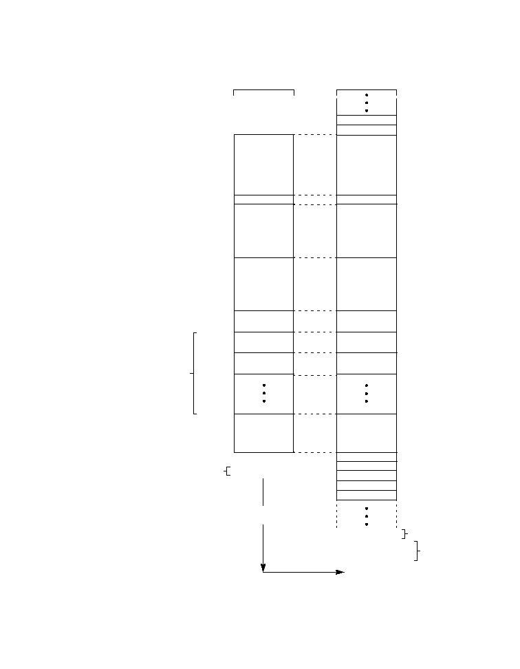
MAC Control Frames
2-45
Copyright � 2000�2001 by LSI Logic Corporation. All rights reserved.
Figure 2.7
Autogenerated Pause Frame Format
Notes:
[1]
< > Means 10B encoded
[2]
/I1/ or /I2/, depends on
running disparity
A[0:7]REG2
A[8:15]REG2
A[16:23]REG1
A[24:31]REG1
A[32:39]REG0
A[40:47]REG0
MAC
10-Bit PHY
10101010
10101010
10101010
10101010
10101010
10101010
10101010
10101011
PRE
SFD
DA
SA
L/T
PARAM
FCS[31:24]
FCS[23:16]
FCS[15:8]
FCS[7:0]
Interface
/I2/
/I2/
/S/
D21.2
D21.2
D21.2
D21.2
D21.2
D21.2
D21.6
[1]
<A[0:7]REG2>
<A[8:15]REG2>
<A[16:23]REG1>
<A[24:31]REG1>
<A[32:39]REG0>
<A[40:47]REG0>
D8.4
D8.0
<FCS[31:24]>
<FCS[23:16]>
<FCS[15:8]>
<FCS[7:0]>
/T/
/R/
/I1/ or /I2/
/I2/
/I2/
a b c d e f g h i j
[2]
MSB
LSB
TX[0]
RX[0]
TX[9]
RX[9]
10-Bit PHY
Interface
PCS 10B
PCS 8B
Bits
Transmitted
Bytes
Transmitted
10000000
00000001
01000011
00000000
00000000
10000000
D1.0
D0.4
D2.6
D0.0
D0.0
D1.0
00010001
00010000
00000000
10000000
OP
P[8:15]REG20
P[0:7]REG20
00000000
00000000
PAD
FCS
(42 Bytes)
DATA
A B C D E F G H
D0.0
D1.0
<P[8:15]REG20>
<P[0:7]REG20>
D0.0
D0.0

2-46
Functional Description
Copyright � 2000�2001 by LSI Logic Corporation. All rights reserved.
2.17.4 Reserved Multicast Address Disable
Receive pause frames are normally rejected as invalid if they do not have
the reserved multicast address in the destination address field. Setting
the MCFLTR bit in
"Register 19�Flow Control 1," Section 4.3.16
,
programs the controller to accept receive pause frames regardless of the
contents in the destination address field. When this bit is cleared, any
value in the destination address field is accepted as a valid address.
2.17.5 MAC Control Frame AutoSend
The level of data in the receive FIFO also triggers the transmission of
autogenerated pause frames. This feature is referred to as MAC control
frame AutoSend. Appropriately setting the MCASEND[3:0] bits in
"Register 19�Flow Control 1," Section 4.3.16
, enable the AutoSend
feature. When MAC control frame AutoSend is enabled, autogenerated
pause frames are transmitted when the receive FIFO data exceeds a
programmable threshold level called the MAC control AutoSend
threshold. The MAC control AutoSend threshold can be set with the four
MACSEND bits in
"Register 19�Flow Control 1," Section 4.3.16
. The
automatic pause frame generation mechanism is described in more
detail in
Section 2.17.1, "Automatic Pause Frame Generation"
.
2.18 Reset
The controller has four resets which are described in
Table 2.13
. The
controller should be ready for normal operation 1
�
s after the reset
sequence has been completed for that bit.

Counters
2-47
Copyright � 2000�2001 by LSI Logic Corporation. All rights reserved.
2.19 Counters
The controller has a set of 53 management counters. Each counter
tabulates the number of times a specific event occurs. A complete list of
all counters along with their definitions is shown in
Table 2.14
. and
described in
Chapter 4, Registers
.These counters provide the necessary
statistics to completely support the following specifications:
�
RMON Statistics Group (IETF RFC1757)
�
SNMP Interfaces Group (IETF RFC1213 and 1573)
�
Ethernet-Like MIB (IETF RFC1643)
�
Ethernet MIB (IEEE 802.3z, clause 30)
Table 2.13
Reset Description
Name
Initiated By
Reset Action
Controller
Reset
RESETn pin
asserted LOW
Reset datapath
Flush transmit FIFO
RST bit = 1 in Register 7
(Configuration i)
Flush receive FIFO
Reset bits to default values
Reset counters to 0
Transmit
Reset
TXRST bit = 1 in Register 7
(Configuration 1)
Reset transmit data path
Flush transmit FIFO
Reset TX counters to 0
Receive
Reset
RXRST bit = 1 in Register 7
(Configuration 1)
Reset receive data
separate path
Flush receive FIFO
Reset RX counters to 0
AutoNegotiation
Restart
ANRST bit = 1 in Register 7
(Configuration 1)
Starts AutoNegotiation
sequence
Counter Reset
CTRRST bit = 1 in Register 7
(Configuration 1)
Reset counters to 0

2-48
Functional Description
Copyright � 2000�2001 by LSI Logic Corporation. All rights reserved.
All counters are 32 bits wide. To obtain each 32-bit counter result,
perform a read operation over the register interface. The address
locations for each counter are shown in both
Table 2.14
and
Table 4.2
.
For the two 16-bit register locations associated with each 32-bit counter,
the register with the lower value address always contains the least
significant 16 bits of the counter result. Thus, C0 of the lower value
address register is the counter LSB; C15 of the higher value address
register is the counter MSB.
When a counter read operation is initiated, the 32-bit counter result to be
accessed is transferred to two internal 16-bit holding registers. These
holding registers freeze and store the counter result for the duration of
the read operation, while allowing the internal counter to continue to
increment if needed.
When a counter is read, the count can, under program control, be
automatically reset to zero or remain unchanged. Counters can be
programmed to either stop counting when they reach their maximum
count or roll over. Burst reading is only supported for the low and high
value address of the same counter. To read the value of multiple
counters, either REGCSn or REGRDn must be deasserted then
reasserted.
Each counter has an associated status bit that is set when the counter
becomes half full. These status bits can be individually programmed to
cause an interrupt.
The counter set in
Table 2.14
includes the packet and octet statistics for
the transmit and receive sides. The RMON specification literally states
that packet and octet counters should only tabulate received information.
This is sometimes interpreted to mean both transmitted and received
information because Ethernet was originally a shared media protocol. As
such, packet and octet counters for both transmit and receive are
available in the controller, and the transmit and receive packet and octet
counts can be summed together if desired.
The exact correspondence of the actual MIB objects from the IETF and
IEEE specifications to the actual controller counters locations is
described in
Chapter 5, Application Information
.

Counters
2-49
Copyright � 2000�2001 by LSI Logic Corporation. All rights reserved.
Table 2.14
Counter Definition
Counter
Number
Counter Name
(MIB Object Name)
Counter Description
RX/TX
Definition
Size
(Bits)
Register
Address
REGAD[7:0]
(Low/High)
RMON Statistics Group MIB (RFC 1757)
1
etherStatsDropEvents
RX
Packets with receive FIFO overflow
error.
32
0b10000000
0b10000001
2
etherStatsOctets
RX
Bytes, exclusive of preamble, in good
or bad packets. Bytes in packets
with bad SFD are excluded.
1
32
0b10000010
0b10000011
3
etherStatsPkts
RX
All packets, good or bad.
1
32
0b10000100
0b10000101
4
etherStatsBroadcastPkts
RX
Broadcast packets, good only.
1
32
0b10000110
0b10000111
5
etherStatsMulticastPkts
RX
Multicast packets, good only.
1
32
0b10001000
0b10001001
6
etherStatsCRCAlignErrors
RX
Packets of legal-length with CRC error
or alignment error.
There are no alignment errors in 8B10B
Gigabit Ethernet, so this counter will
only count CRC errors for legal length
packets.
32
0b10001010
0b10001011
7
etherStatsUndersizePkts
RX
Packets of length < 64 bytes with no
other errors.
32
0b10001100
0b10001101
8
etherStatsOversizePkts
RX
Packets of length > Max_Packet_Length
with no other errors.
32
0b10001110
0b10001111
9
etherStatsFragments
RX
Packets of length < 64 bytes with CRC
error or alignment error.
There are no alignment errors in 8B10B
Gigabit Ethernet, so this counter will
only count CRC errors with length < 64.
32
0b10010000
0b10010001
10
etherStatsJabber
RX
Packets of length > Max_Packet_Length
with CRC error or alignment error.
There is no jabber function in Gigabit
Ethernet, so this counter is undefined.
32
0b10010010
0b10010011

2-50
Functional Description
Copyright � 2000�2001 by LSI Logic Corporation. All rights reserved.
11
etherStatsCollisions
TX/
RX
CRS asserted and one or more
collsions occurred.
Since controller is Full Duplex only,
this counter is undefined.
32
0b10010100
0b10010101
12
etherStatsPkts64Octets
RX
Packets of length = 64 bytes, good or
bad.
1
32
0b10010110
0b10010111
13
etherStatsPkts65to127Octets
RX
Packets of length between 65�127
bytes, inclusive, good or bad.
1
32
0b10011000
0b10011001
14
etherStatsPkts128to255Octets
RX
Packets of length between 128�255
bytes, inclusive, good or bad.
1
32
0b10011010
0b10011011
15
etherStatsPkts256to511Octets
RX
Packets of length between 256�511
bytes, inclusive, good or bad.
1
32
0b10011100
0b10011101
16
etherStatsPkts512to1023Octets
RX
Packets of length between 512�1023
bytes, inclusive, good or bad.
1
32
0b10011110
0b10011111
17
etherStatsPkts1024to1518Octets
RX
Packets of length between 1024 and
Max_Packet_Length, inclusive, or bad.
1
32
0b10100000
0b10100001
18
etherStatsOctets_TX
TX
Bytes, exclusive of preamble,
in good or bad packets.
1
32
0b10100010
0b10100011
19
etherStatsPkts_TX
TX
All packets, good or bad.
1
32
0b10100100
0b10100101
20
etherStatsBroadcastPkts_TX
TX
Broadcast packets, good only.
1
32
0b10100110
0b10100111
21
etherStatsMulticastPkts_TX
TX
Multicast packets, good only.
1
32
0b10101000
0b10101001
22
etherStatsPkts64Octets_TX
TX
Packets of length = 64 bytes, good or
bad.
1
32
0b10101010
0b10101011
23
etherStatsPkts65to127Octets_TX
TX
Packets of length between 65�127
bytes, inclusive, good or bad.
1
32
0b10101100
0b10101101
24
etherStatsPkts128to255Octets_TX
TX
Packets of length between 128�255,
inclusive, good or bad.
1
32
0b10101110
0b10101111
25
etherStatsPkts256to511Octets_TX
TX
Packets of length between 256�511
bytes, inclusive, good or bad.
1
32
0b10110000
0b10110001
Table 2.14
Counter Definition (Cont.)
Counter
Number
Counter Name
(MIB Object Name)
Counter Description
RX/TX
Definition
Size
(Bits)
Register
Address
REGAD[7:0]
(Low/High)

Counters
2-51
Copyright � 2000�2001 by LSI Logic Corporation. All rights reserved.
26
etherStatsPkts512to1023Octets_TX
TX
Packets of length between 512�1023
bytes, inclusive, good or bad.
1
32
0b10110010
0b10110011
27
etherStatsPkts1024to1518Octets_
TX
TX
Packets of length between 1023
and Max_Packet _Length,
inclusive, good or bad.
1
32
0b10110100
0b10110101
SNMP Interfaces Group MIB (RFC 1213 & 1573)
28
ifInOctets
RX
Bytes, including preamble,
in good or bad packets.
32
0b10110110
0b10110111
29
ifInUcastPkts
RX
Unicast packets, good only.
32
0b10111000
0b10111001
ifInMulticastPkts
RX
Multicast packets, good only.
Equivalent to "etherStatsMulticastPkts"
Use Ctr. #5
ifInBroadcastPkts
RX
Broadcast packets, good only.
Equivalent to "etherStatsBroadcastPkts"
Use Ctr. #4
ifInNUcastPkts
RX
Broadcast and multicast packets, good
only.
Equivalent to "etherStatsBroadcastPkts
+ etherStatsMulticastPkts"
Use Ctr. #4
and 5
ifInDiscards
RX
Packets with receive FIFO overflow
error.
Equivalent to "etherStatsDropEvents"
Use Ctr. #1
ifInErrors
RX
All packets, bad only.
Equivalent to "etherStatsCRCAlignError
+ etherStatsUndersizePkts +
etherStatsOversizePkts"
Use Ctr. #6
and 7 and 8
30
ifOutOctets
TX
Bytes, including preamble,
in good or bad packets.
32
0b10111010
0b10111011
31
ifOutUcastPkts
TX
Unicast packets, good and bad.
32
0b10111100
0b10111101
32
ifOutMulticastPkts
TX
Multicast packets, good and bad.
32
0b10111110
0b10111111
Table 2.14
Counter Definition (Cont.)
Counter
Number
Counter Name
(MIB Object Name)
Counter Description
RX/TX
Definition
Size
(Bits)
Register
Address
REGAD[7:0]
(Low/High)

2-52
Functional Description
Copyright � 2000�2001 by LSI Logic Corporation. All rights reserved.
33
ifOutBroadcastPkts
TX
Broadcast packets, good and bad.
32
0b11000000
0b11000001
ifOutNUcastPkts
TX
Broadcast and multicast packets,
good and bad.
Equivalent to "ifOutMulticastPkts +
ifOutBroadcastPkts"
Use Ctr.
#32 and 33
34
ifOutDiscards
TX
Packets with transmit FIFO underflow
error.
32
0b11000010
0b11000011
35
ifOutErrors
TX
All Packets, bad only,
exclusive of legal-length errors.
32
0b11000100
0b11000101
Ethernet-Like Group MIB
(RFC 1643)
36
dot3StatsAlignmentErrors
RX
Packets with alignment error only.
There are no alignment errors in
8B10B Gigabit Ethernet,
so this counter is undefined.
32
0b11000110
0b11000111
dot3StatsFCSErrors
RX
Packets with CRC error only.
Equivalent to
"etherStatsCRCAlignErrors"
Use Ctr. #6
38
dot3StatsSingleCollisionFrames
TX
Packets successfully transmitted after
one and only one collision (ie: attempt
value = 2).
Since controller is Full Duplex only,
this counter is undefined.
32
0b11001010
0b11001011
39
dot3StatsMultipleCollisionFrames
TX
Packets successfully transmitted after
more than one collision (ie: 2<attempt
value<16).
Since controller is Full Duplex only,
this counter is undefined.
32
0b11001100
0b11001101
40
dot3StatsSQETestErrors
RX
Number of times SQE was asserted.
There is no SQE for Gigabit Ethernet,
so this counter is undefined.
32
0b11001110
0b11001111
41
dot3StatsDeferredTransmissions
TX
Packets deferred, i.e. packets whose
transmission was delayed due to busy
medium, on first attempt only.
Since controller is Full Duplex only,
this counter is undefined.
32
0b11010000
0b11010001
Table 2.14
Counter Definition (Cont.)
Counter
Number
Counter Name
(MIB Object Name)
Counter Description
RX/TX
Definition
Size
(Bits)
Register
Address
REGAD[7:0]
(Low/High)

Counters
2-53
Copyright � 2000�2001 by LSI Logic Corporation. All rights reserved.
42
dot3StatsLateCollisions
TX
Packets that encounter a late collision,
i.e. encountered collisions more than
512-bit times into transmitted packet.
A late collision is counted twice:
as a collision and a late collision.
Since controller is Full Duplex only,
this counter is undefined.
32
0b11010010
0b11010011
43
dot3StatsExcessiveCollisions
TX
Packets not successfully transmitted
after more than 15 collisions
(ie: attempt value=16).
Since controller is Full Duplex only,
this counter is undefined.
32
0b11010100
0b11010101
dot3StatsInternalMacTransmitErrors
TX
Packets with transmit FIFO underflow
error.
Equivalent to "ifOutDiscards"
Use Ctr. #34
44
dot3StatsCarrierSenseErrors
TX
Carrier sense dropout errors, i.e.
number of times that carrier sense is
not asserted or deasserted during
packet transmission, without a collision.
This counter is only incremented once
per packet, regardless of the number of
dropout errors in the packet.
There is no CRS loopback in 8B10B
Ethernet, so this counter is undefined.
32
0b11010110
0b11010111
dot3StatsFrameTooLongs
RX
Packets of length > Max_Packet_Length
with no other errors.
Equivalent to "etherStatsOversizePkts"
Use Ctr. #8
dot3StatsInternalMacReceiveErrors
RX
Packets with receive FIFO overflow
error.
Equivalent to "etherStatsDropEvents"
Use Ctr. #1
Ethernet MIB
(IEEE 802.3z Clause 30)
44
aFramesTransmittedOK
TX
All packets, good only.
Equivalent to
"etherStatsPkts_TX - ifOutErrors"
32
Use Ctr.
#19 through
35
aSingleCollisionFrames
TX
Packets successfully transmitted after
one and only one collision (ie: attempt
value = 2).
Equivalent to
"dot3StatsSingleCollisionFrames"
Use Ctr. #38
Table 2.14
Counter Definition (Cont.)
Counter
Number
Counter Name
(MIB Object Name)
Counter Description
RX/TX
Definition
Size
(Bits)
Register
Address
REGAD[7:0]
(Low/High)

2-54
Functional Description
Copyright � 2000�2001 by LSI Logic Corporation. All rights reserved.
44
aMultipleCollisionFrames
TX
Packets successfully transmitted after
more than one collision (ie: 2<attempt
value <16).
Equivalent to
"dot3StatsMultipleCollisionFrames"
32
Use Ctr. #39
aFramesReceivedOK
RX
All packets, good only.
Equivalent to "ifInUcastPkts +
etherStatsBroadcastPkts +
etherStatsMulticastPkts"
Use Ctr. #29
and 4 and 5
aFrameCheckSequenceErrors
RX
Packets with CRC error only.
Equivalent to "dot3StatsFCSErrors"
Use Ctr. #37
aAlignmentErrors
RX
Packets with alignment error only.
Equivalent to
"dot3StatsAlignmentErrors"
Use Ctr. #36
45
aOctetsTransmittedOK
TX
Bytes, exclusive of preamble,
in good packets only.
32
0b11011000
0b11011001
aFramesWithDeferredXmissions
TX
Packets deferred, i.e. packets whose
transmission was delayed due to busy
medium, on first attempt only.
Equivalent to
"dot3StatsDeferredTransmissions"
Use Ctr. #41
aLateCollisions
TX
Packets that encounter a late collision,
i.e. encountered collisions more than
512-bit times into transmitted packet.
A late collision is counted twice,
as a collision and a late collision.
Equivalent to "dot3StatsLateCollisions"
Use Ctr. #42
aFrameAbortedDueToXSCollisions
TX
Packets not successfully transmitted
after more than 15 collisions
(ie: attempt value=16).
Equivalent to
"dot3StatsExcessiveCollisions"
Use Ctr. #43
aFrameAbortedDueToIntMACXmit
Error
TX
Packets with transmit FIFO underflow
error.
Equivalent to "ifOutDiscards"
Use Ctr. #34
Table 2.14
Counter Definition (Cont.)
Counter
Number
Counter Name
(MIB Object Name)
Counter Description
RX/TX
Definition
Size
(Bits)
Register
Address
REGAD[7:0]
(Low/High)

Counters
2-55
Copyright � 2000�2001 by LSI Logic Corporation. All rights reserved.
45
aCarrierSenseErrors
TX
Carrier sense dropout errors, i.e.
number of times that carrier sense is
not asserted or deasserted during
packet transmission, without a collision.
This counter is only incremented once
per packet, regardless of the number of
dropout errors in the packet.
Equivalent to
"dot3StatsCarrierSenseErrors"
32
Use Ctr. #44
46
aOctetsReceivedOK
RX
Bytes, exclusive of preamble,
in good packets only.
32
0b11011010
0b11011011
aFramesLostDueToIntMACRcvr
Error
RX
Packets with receive FIFO overflow
error.
Equivalent to "etherStatsDropEvents"
Use Ctr. #1
aMulticastFrameXmittedOK
TX
TX Multicast packets, good only.
Equivalent to
"etherStatsMulticastPkts_TX"
Use Ctr. #21
aBroadcastFramesXmittedOK
TX
TX Broadcast packets, good only.
Equivalent to
"etherStatsBroadcastPkts_TX"
Use Ctr. #20
47
aFramesWithExcessiveDefferal
TX
Packets with excessive deferral,
i.e. packets waiting for transmission
longer than two max packet times.
Since controller is Full Duplex only,
this counter is undefined.
32
0b11011100
0b11011101
aMulticastFramesReceivedOK
RX
Multicast packets, good only.
Equivalent to "etherStatsMulticastPkts"
Use Ctr. #5
aBroadcastFramesReceivedOK
RX
Broadcast packets, good only.
Equivalent to "etherStatsBroadcastPkts"
Use Ctr. #4
48
aInRangeLengthErrors
RX
Packets of legal-length whose actual
length is different from length/type field
value.
32
0b11011110
0b11011111
49
aOutOfRangeLengthField
RX
Packets with length/type
field value > Max_Packet_Length.
32
0b11100000
0b11100001
aFrameTooLongErrors
RX
Packets of length > Max_Packet_Length
with no other errors.
Equivalent to "etherStatsOversizePkts"
Use Ctr. #8
Table 2.14
Counter Definition (Cont.)
Counter
Number
Counter Name
(MIB Object Name)
Counter Description
RX/TX
Definition
Size
(Bits)
Register
Address
REGAD[7:0]
(Low/High)

2-56
Functional Description
Copyright � 2000�2001 by LSI Logic Corporation. All rights reserved.
a. Bad RX packet = legal-length error, CRC error, receive FIFO overflow, symbol error.
Where: CRC Error is bad FCS with an integral number of octets. Alignment Error is bad FCS with
nonintegral number of octets. Symbol Error is an invalid codeword or a /V/.
b. Bad TX packet = legal-length error, transmit FIFO underflow.
c. Legal-length packet is between 64 and Max_Packet_Length in bytes. Preamble is not included
in length count.
d. Max_Packet_Length for the counters can be programmed to be either 1518, 1522, 1535, or
unlimited bytes. 1518 is the default for both transmit and receive.
e. The counter result is stored in two 16-bit registers. Thus, there are two register addresses for
each counter. Of the two registers for a given counter, the register with the lower value address
contains the least significant counter bits.
f. The RMON specs explicitly states that packet and octet counters should only tabulate received
information. This is sometimes interpreted to mean both transmitted and received information
because Ethernet was originally a shared media. As such, transmit packet and octet counters are
also available in counters 18�27 and can be summed with receive packet and octet counts if
desired.
49
aSQETestErrors
RX
Number of times SQE was asserted.
Equivalent to "dot3StatsSQETestError"
32
Use Ctr. #40
50
aSymbolErrorDuringCarrier
RX
One or more symbol errors received
from a PHY during packet reception,
exclusive of collision. This counter is
only incremented once per packet,
regardless of the number
of symbol errors in that packet.
32
0b11100010
0b11100011
aMACControlFramesTransmitted
TX
Valid MAC Control packets.
Equivalent to
"apauseMACCtrlFramesTransmitted"
Use Ctr. #52
aMACControlFramesReceived
RX
Valid MAC Control packets.
Equivalent to
"apauseMACCtrlFramesReceived"
Use Ctr. #53
51
aUnsupportedOpcodesReceived
RX
Valid MAC Control packets
with non-pause opcode.
32
0b11100100
0b11100101
52
apauseMACCtrlFramesTransmitted
TX
Valid MAC Control packets
with pause opcode.
32
0b11100110
0b11100111
53
apauseMACCtrlFramesReceived
RX
Valid MAC Control packets
with pause opcode.
32
0b11101000
0b11101001
1. Footnotes
Table 2.14
Counter Definition (Cont.)
Counter
Number
Counter Name
(MIB Object Name)
Counter Description
RX/TX
Definition
Size
(Bits)
Register
Address
REGAD[7:0]
(Low/High)

Counters
2-57
Copyright � 2000�2001 by LSI Logic Corporation. All rights reserved.
2.19.1 Counter Half Full
Each 32-bit counter has a half-full status output bit associated with it.
The half-full bits are stored in
"Register 112�115�Counter Half Full 1-4,"
Section 4.3.23
. A half-full bit is set when its counter value reaches
0x80000000 (MSB bit goes from a 0 to a 1), so it is set when the counter
becomes half full.
The counter half-full bits latch themselves when they are set. Each bit
stays latched until either the bit is read or the counter register with which
the bit is associated is read. Counter half-full bits are also interrupt bits
(the setting of any counter half-full bit can be programmed to cause the
assertion of the interrupt pin, REGINT). When a read clears the counter
half-full bit, the interrupt is also cleared.
Note:
REGINT stays asserted until all interrupt bits are cleared.
Each counter half-full bit can be individually programmed to assert (or
not assert) the REGINT pin. Setting the appropriate mask bit associated
with the counter half full
"Registers 120�123�Counter Half Full Mask 1-
4," Section 4.3.24
, programs the controller to mask (disable) the interrupt
caused by the corresponding counter half full detect bit.
2.19.2 Counter Reset On Read
A read operation on a counter does not normally affect the counter
values. However, setting the CTR_RD bit in
"Register 9�Configuration 3,"
Section 4.3.10
, programs the counter to automatically reset to zero when
read.
When the CTR_RD bit is set, a counter is cleared to 0 whenever any one
of the two 16-bit counter registers associated with a 32-bit counter is
read. An internal holding register stores the entire 32-bit counter result
so that the result is correctly read as long as two successive 16-bit
counter register reads are performed from the same counter. In order to
read the cleared value, the read operation needs to be deasserted then
reasserted (i.e., REGCSn and REGRDn).
When the CTR_RD bit is cleared (default), a read does not affect the
count in the counter, as long as the counter is not at maximum count. If
a counter is at maximum count, its count is always reset to 0 when the
counter is read.

2-58
Functional Description
Copyright � 2000�2001 by LSI Logic Corporation. All rights reserved.
2.19.3 Counter Rollover
Counters normally roll over to zero when they exceed their maximum
count, (receive an increment when counter is at maximum count). The
counters can be programmed to freeze and stop counting once they
reach their maximum count. Setting the CTR_ROLL bit in
"Register 9�
Configuration 3," Section 4.3.10
, programs the counters to freeze when
they reach their maximum count.
2.19.4 Counter Maximum Packet Size
The maximum packet size used for the management counter statistics
can be programmed to be one of four values. Setting the CMXPKT[1:0]
bits in
"Register 10�Configuration 4," Section 4.3.11
, select the maximum
packet size. This selection is described in the register descriptions for
those registers and is also summarized in
Table 2.15
.
The bits in
Table 2.15
affect the maximum packet size for the counters
only; the maximum packet size for the MAC section is described in
Section 2.8, "Receive MAC"
.
2.19.5 Counter Reset
Setting the CTRRST bit in
"Register 7�Configuration 1," Section 4.3.8
,
resets all counters to zero. Asserting the controller reset pin, RESETn,
also resets the counters to zero.
Table 2.15
Counter Maximum Packet Size Selection
CMXPKT [1:0]
Maximum Packet Size (bytes)
11
Unlimited
10
1535
01
1522
00
1518

Loopback
2-59
Copyright � 2000�2001 by LSI Logic Corporation. All rights reserved.
2.20 Loopback
To enable the diagnostic loopback mode, set the LPBK bit in
"Register
10�Configuration 4," Section 4.3.11
. When the loopback mode is
enabled, the transmit data input to the transmit system interface and
output from the 8B10B encoder is internally looped back into the receive
8B10B decoder and is available to be read from the receive system
interface.
2.21 Test Modes
The TEST pin is reserved for factory test, and must be tied LOW for
normal operation.
Asserting the TAP pin HIGH, sets all inputs and outputs in the
high-impedance state. This pin is intended for controller and board
diagnostic testing.

2-60
Functional Description
Copyright � 2000�2001 by LSI Logic Corporation. All rights reserved.

8101/8104 Gigabit Ethernet Controller
3-1
Copyright � 2000�2001 by LSI Logic Corporation. All rights reserved.
Chapter 3
Signal Descriptions
This chapter describes the 8101/8104 Gigabit Ethernet Controller signals
in the following sections:
�
Section 3.1, "System Interface Signals"
�
Section 3.2, "10-Bit PHY Interface Signals"
�
Section 3.3, "Register Interface Signals"
�
Section 3.4, "Micellaneous Signals"
�
Section 3.5, "Power Supply Signals"
Figure 3.1
is a diagram of the 8101/8104 signals.

3-2
Signal Descriptions
Copyright � 2000�2001 by LSI Logic Corporation. All rights reserved.
Figure 3.1
8101/8104 Interface Diagram
SCLK
TXENn
TXD[31:0]
TXBE[3:0]
TXSOF
TXEOF
TXWM1n
TXWM2n
TXDC
CLR_TXDC
FCNTRL
TXCRCn
RXENn
RXOEn
RXD[31:0]
RXBE[3:0]
RXSOF
RXEOF
RXWM1
RXWM2
RXDC
CLR_RXDC
RXABORT
System
Interface
TBC
TX[9:0]]
RBC[1:0]
RX[9:0]
EN_CDET
EWRAP
LCK_REFn
REGCSn
REGCLK
REGD[15:0]
REGA[7:0]
REGRDn
REGWRn
REGINT
TCLK
LINKn
SD
RESETn
TAP
TEST
VCC
GND[30:0]
10-Bit PHY
Interface
Register
Interface
Miscellaneous
3.3 V
�
5%
Ground

System Interface Signals
3-3
Copyright � 2000�2001 by LSI Logic Corporation. All rights reserved.
3.1 System Interface Signals
This section describes the 8101/8104 system interface signals.
CLR_RXDC
Clear RXDC
Input
When CLR_RXDC is asserted, the RXDC pin is cleared.
Wheh CLR_RXDC is LOW, the RXDC pin is not cleared.
CLR_RXDC is clocked in on the rising edge of the
system clock, SCLK.
This pin only clears RXDC when AutoClear mode is
disabled. When AutoClear mode is enabled, this pin is
ignored and RXDC is automatically cleared two clock
cycles after RXEOF is asserted.
CLR_TXDC
Clear TXDC
Input
When CLR_TXDC is HIGH, the TXDC pin is cleared.
When CLR_TXDC is LOW, the TXDC pin is not cleared.
TXDC is clocked in on the rising edge of the system
clock, SCLK.
This pin only clears TXDC when AutoClear mode is
disabled. When AutoClear mode is enabled, this pin is
ignored and TXDC is automatically cleared two clock
cycles after TXEOF is asserted.
FCNTRL
Flow Control Enable
Input
When FCNTRL is HIGH, transmitter automatically
transmits a MAC control pause frame. When FCNTRL is
LOW, the controller resumes normal operation. FCNTRL
is clocked in on the rising edge of the system clock,
SCLK.
RXABORT
Receive FIFO Data Abort
Input
When RXABORT is asserted, the packet being read out
on RXD[31:0] is aborted and discarded. When LOW, the
packet is not aborted and discarded. RXABORT is
clocked in on the rising edge of the system clock, SCLK.
RXBE[3:0]
Receive Byte Enable
Output
These outputs determine which bytes of the current data
on RXD[31:0] contain valid data. RXBE[3:0] is clocked
out of the device on the rising edge of the system
interface clock, SCLK.

3-4
Signal Descriptions
Copyright � 2000�2001 by LSI Logic Corporation. All rights reserved.
RXD[31:0]
Receive Data
Output
This output bus contains the 32-bit received data word
that is clocked out on the rising edge of the system
interface clock, SCLK.
RXDC
Receive Packet Discard
Output
When HIGH, device detects that current packet being
output on the system interface has an error and should
be discarded. When LOW, no discard.
Asserting the RXABORT pin or setting the AUTORXAB
bit in
"Register 9�Configuration 3," Section 4.3.10
,
automatically discards the packet being output. RXDC is
clocked out on the rising edge of the system clock, SCLK.
If AutoClear mode is not enabled, this output is latched
HIGH and stays latched until cleared with the assertion
of the CLR_RXDC pin. If AutoClear mode is enabled, this
output is latched HIGH and automatically clears itself
LOW two clock cycles after RXEOF is asserted. RXDC
can also be cleared with RXABORT if programmed to do
so.
RXENn
Receive Enable
Input
This input must be asserted active LOW to enable the
current data word to be clocked out of the receive FIFO
on RXD[31:0]. RXENn is clocked in on the rising edge of
the system interface clock, SCLK.
RXEOF
Receive End Of Frame
Output
This output is asserted on the same clock cycle as the
last word of the packet is being read out of the receive
FIFO on RXD[31:0]. RXEOF is clocked out of the device
on the rising edge of the system interface clock, SCLK.
RXOEn
Receive Output Enable
Input
When LOW, all receive outputs are active. When HIGH,
receive outputs (RXD[31:0], RXBE[3:0], RXSOF, RXEOF)
are high-impedence.
RXSOF
Receive Start Of Frame
Output
This output is asserted on the same clock cycle as the
first word of the packet is being read out of the receive
FIFO on RXD[31:0]. RXSOF is clocked out of the device
on the rising edge of the system interface clock, SCLK.

System Interface Signals
3-5
Copyright � 2000�2001 by LSI Logic Corporation. All rights reserved.
RXWM1
Receive FIFO Watermark 1
Output
When RXWM1 is LOW, the receive FIFO data is less
than or equal to the receive FIFO watermark 1 threshold.
When HIGH, the receive FIFO data is greater than the
watermark. RXWM1 is clocked out on the rising edge of
the system clock, SCLK. Data is valid on RXD[31:0] when
either RXWM1 or RXWM2 is asserted, independent of
RXENn.
RXWM2
Receive FIFO Watermark 2
Output
When RXWM2 is LOW, the receive FIFO data is less
than or equal to the receive FIFO watermark 2 threshold
and no EOF in FIFO. When HIGH, the receive FIFO data
is greater than the watermark. RXWM2 is clocked out on
the rising edge of the system clock, SCLK. Data is valid
on RXD[31:0] when either RXWM1 or RXWM2 is
asserted, independent of RXENn.
SCLK
System Interface Clock
Input
This input clocks data in and out of the transmit and
receive FIFOs on TXD[31:0] and RXD[31:0], respectively.
All system interface inputs and outputs are also clocked
in and out on the rising edge of SCLK, with the exception
of RXOEn. SCLK clock frequency must be between
33�66 MHz.
TXBE[3:0]
Transmit Byte Enable
Input
These inputs determine which bytes of the current 32-bit
word on TXD[31:0] contain valid data. TXBE[3:0] is
clocked into the device on the rising edge of the system
interface clock, SCLK.
TXCRCn
Transmit CRC Enable
Input
When TXCRC is LOW, CRC is calculated and appended
to the current packet being input on the system interface.
When TXCRC is HIGH, CRC is not calculated. TXCRCn
is clocked in on the rising edge of the system clock,
SCLK, and must be asserted on the same SCLK clock
cycle as TXSOF.
TXD[31:0]
Transmit Data
Input
This input bus contains the 32-bit data word that is
clocked into the transmit FIFO on the rising edge of the
system interface clock, SCLK.

3-6
Signal Descriptions
Copyright � 2000�2001 by LSI Logic Corporation. All rights reserved.
TXDC
Transmit Packet Discard
Output
When TXDC is HIGH, the controller detects that current
packet being input on the system interface has an error,
rest of packet ignored. When LOW, The packet is not
discarded. TXDC is clocked out on thr rising edge of the
system clock.
If AutoClear mode is not enabled, this output is latched
HIGH and stays latched until cleared with the assertion
of the CLR_TXDC pin. If AutoClear mode is enabled, this
output is latched HIGH and automatically clears itself
LOW two clock cycles after TXEOF is asserted.
TXENn
Transmit Enable
Input
This input must be low to enable the current data word
on TXD[31:0] to be clocked into the transmit FIFO.
TXENn is clocked in on the rising edge of the system
interface clock, SCLK.
TXEOF
Transmit End Of Frame
Input
This input must be asserted on the same clock cycle as
the last word of the packet is being clocked in on
TXD[31:0]. TXEOF is clocked into the device on the rising
edge of the system interface clock, SCLK.
TXSOF
Transmit Start Of Frame
Input
This input must be asserted on the same clock cycle as
the first word of the packet is being clocked in on
TXD[31:0]. TXSOF is clocked into the device on the rising
edge of the system interface clock, SCLK.
TXWM1n
Transmit FIFO Watermark 1
Output
When TXWM1n is HIGH, the transmit FIFO data is less
than or equal to the transmit FIFO watermark 1. When
LOW, the transmit FIFO data is above the watermark.
TXWM1n is clocked out on the rising edge of the system
clock, SCLK.
TXWM2n
Transmit FIFO Watermark 2
Output
When TXWM2n is HIGH, the transmit FIFO data is less
than or equal to the transmit FIFO watermark 2. When
LOW, the transmit FIFO data is above the watermark.
TXWM2n is clocked out on the rising edge of the system
clock, SCLK.

10-Bit PHY Interface Signals
3-7
Copyright � 2000�2001 by LSI Logic Corporation. All rights reserved.
3.2 10-Bit PHY Interface Signals
This section describes the 8101/8104 10-Bit PHY interface signals.
EN_CDET
Comma Detect Enable
Output
This output is asserted when either the receive 8B10B
PCS state machine is in the loss of synchronization state
or the CDET bit is set in
"Register 9�Configuration 3,"
Section 4.3.10
. This output is typically used to enable the
comma detect function in an external physical layer
device.
EWRAP
Loopback Output Enable
Output
This output is asserted whenever the EWRAP bit is set
in
"Register 9�Configuration 3," Section 4.3.10
. This
output is typically used to enable loopback in an external
physical layer device.
LCK_REFn
Receiver Lock
Output
This output is asserted whenever the LCK_REFn bit is
set in
"Register 9�Configuration 3," Section 4.3.10
. This
output is typically used to enable the receive
lock-to-reference mechanism in an external physical
layer.
RBC[1:0]
Receive Clock
Input
The RBC[1:0] signals clock receive data into the
controller on the clock rising edge. RBC[1:0] are
62.5 MHz clocks, 180
�
out of phase, that clock data into
the controller on RX[9:0] at an effective rate of 125 MHz.
For the device to acquire synchronization, the comma
code must be input on RXD[9:0] on RBC1 rising edges.
RX[9:0]
Receive Data
Input
These inputs contain receive data that are clocked in on
the rising edges of RBC[1:0].
TBC
Transmit Clock
Output
This output clock transmits data out on TX[0:9] on its
rising edge. TBC is a 125 MHz clock and is generated
from TCLK.

3-8
Signal Descriptions
Copyright � 2000�2001 by LSI Logic Corporation. All rights reserved.
TX[9:0]
Transmit Data
Output
These interface outputs transmit data on the rising edge
of TBC.
3.3 Register Interface Signals
This section describes the 8101/8104 register interface signals.
REGA[7:0]
Register Interface Address
Input
These inputs provide the address for the specific internal
register to be accessed, and are clocked into the device
on the rising edge of REGCLK.
REGCLK
Register Interface Clock
Input
This input clocks data in and out on REGD[15:0],
REGA[7:0], REGRDn, and REGWRn on its rising edge.
REGCLK frequency must be between 5�40 MHz.
REGCSn
Register Interface Chip Select
Input
This input must be asserted to enable reading and writing
data on REGD[15:0] and REGA[7:0]. This input is
clocked in on the rising edge of REGCLK.
REGD[15:0]
Register Interface Data Bus
Bidirectional
This bus is a bidirectional 16-bit data path to and from the
internal registers. Data is read and written from and to
the internal registers on the rising edge of the register
clock, REGCLK.
REGINT
Register Interface Interrupt
Output
This output is asserted when certain interrupt bits in the
registers are set, and it remains latched HIGH until all
interrupt bits are read and cleared.
REGRDn
Register Interface Read
Input
When this input is asserted, the accessed internal
register is read (data is output from the register). This
input is clocked into the device on the rising edge of
REGCLK.
REGWRn
Register Interface Write
Input
When this input is asserted, the accessed internal
register is written (data is input to the register). This input
is clocked into the device on the rising edge of REGCLK.

Micellaneous Signals
3-9
Copyright � 2000�2001 by LSI Logic Corporation. All rights reserved.
3.4 Micellaneous Signals
This section describes the 8101/8104 micellaneous signals.
LINKn
Receive Link
Output
When this signal is HGH, there is no link. When this
signal is asserted, the receive link is synchronized and
configured.
RESERVED
Reserved
These pins are reserved and must be left floating.
RESETn
Reset
Input
When this signal is HIGH, controller is in normal
operation. When this signal is asserted, controller resets,
FIFO's are cleared, counters are cleared, and register
bits are set to default values.
SD
Signal Detect
Input
When this signal is asserted, data detected on receive
10-bit PHY is valid. When SD is LOW, data is not valid
and the 8B10B PCS receiver is forced to a loss of sync
state. This signal is ignored (assumed high) unless the
SD_EN bit in
"Register 9�Configuration 3,"
Section 4.3.10
, is cleared.
TAP
3-state all pins
Input
This pin is used for testing purposes only. When
asserted, all output and bidirectional pins are placed in a
high-impedence state.
TEST
Test Mode
Input
This pin is used for factory test and must be tied LOW for
proper operation.
TCLK
Transmit Clock
Input
This 125 MHz input clock is used by the 8B10B PCS
section and generates the 125 MHz transmit output clock,
TBC, is used to output data on the 10-bit PHY interface.

3-10
Signal Descriptions
Copyright � 2000�2001 by LSI Logic Corporation. All rights reserved.
3.5 Power Supply Signals
This section describes the 8101/8104 power supply signals.
VCC[26:0]
Positive Supply.
�
+3.3 V
�
5% Volts
GND[26:0]
Ground
�
0 Volts

8101/8104 Gigabit Ethernet Controller
4-1
Copyright � 2000�2001 by LSI Logic Corporation. All rights reserved.
Chapter 4
Registers
The 8101/8104 controller has 136 internal 16-bit registers. Twenty-two
registers are available for setting configuration inputs and reading status
outputs. The remaining 114 registers are associated with the
management counters.
This chapter contains the following sections:
�
Section 4.1, "Register Interface"
�
Section 4.2, "Register Addresses"
�
Section 4.3, "Register Definitions"
4.1 Register Interface
The register interface is a 16-bit bidirectional data interface that allows
access to the internal registers. The register interface consists of 29
signals:
�
Sixteen bidirectional data I/O bits (REGD[15:0])
�
Eight register address inputs (REGA[7:0])
�
One chip select input (REGCSn)
�
One clock input (REGCLK) The REGCLK clock frequency must be
between 5
-
40 MHz.
�
One read select input (REGRDn)
�
One write select input (REGWRn)
�
One interrupt output (REGINT)
All register accesses are done on the rising edge of the REGCLK clock.
To access a register through the register interface, REGCSn must be
asserted and is sampled on the rising edge of REGCLK. On that same

4-2
Registers
Copyright � 2000�2001 by LSI Logic Corporation. All rights reserved.
rising edge of REGCLK, the address of the register that is accessed is
clocked in on REGA[7:0]. On that same rising edge of REGCLK, either
REGRDn or REGWRn must also be asserted. These signals determine
whether the register access is a read or write cycle. During a write cycle,
the data to be written to a specific register is clocked in on the rising
edge of the same clock that clocked in the other inputs. During a read
cycle, the data is output on REGD[15:0] some delay after the rising edge
of REGCLK that clocked in the input information. REGCSn can remain
LOW for multiple REGCLK cycles so that many registers can be read or
written during one REGCSn assertion.
During read cycles, the delay from REGCLK to data valid on the
REGD[15:0] pins is a function of which register is being accessed. Data
read from any register, exclusive of the Counter 1
-
53 registers, appears
on the REGD[15:0] pins in one REGCLK cycle. Data read from the
Counter 1
-
53 registers takes at most six REGCLK cycles to be available
on REGD[15:0] for the first 16 bits of the counter result, and at most
three REGCLK cycles for the second 16 bits of the counter result. Refer
to
Chapter 6, Specifications
for details of the interface timing
characteristics.
4.1.1 Bit Types
The register interface is bidirectional, and there are many types of bits in
the registers. The bit type definitions are summarized in
Table 4.1
. Write
bits (W) are inputs during a write cycle and are 0 during read cycles.
Read bits (R) are outputs during a read cycle and ignored and high-
impedance during a write cycle. Read/Write bits (R/W) are actually write
bits that can be read during a read cycle. R/WSC bits are R/W bits that
are self clearing after a set period of time or after a specific event has
completed. R/LL bits are read bits that latch themselves when they go to
0 and they stay latched until read. After they are read, they are set to 1.
R/LH bits are the same as R/LL bits except that they latch to 1. R/LT are
read bits that latch themselves whenever they make a transition or
change value and they stay latched until they are read. After R/LT bits
are read, they are updated to their current value. R/LLI, R/LHI, and R/LTI
bits function the same as R/LL, R/LH and R/LT bits, respectively, except
they also assert interrupt if programmed to do so (not masked).

Register Interface
4-3
Copyright � 2000�2001 by LSI Logic Corporation. All rights reserved.
4.1.2 Interrupt
An interrupt is triggered when certain output status bits change state.
These bits are called interrupt bits and are designated as R/LLI, R/LHI,
and R/LTI bits, as described in the previous section. The interrupt bits
reside in
"Register 11�Status 1," Section 4.3.12,
and
"Register 112�115�
Counter Half Full 1-4," Section 4.3.23,
. Interrupt bits automatically latch
Table 4.1
Register Bit Type Definition
Bit Types
Definition
Symbol
Name
Write Cycle
Read Cycle
W
Write
Input
No operation, output not valid
R
Read
No operation, input ignored
Output
R/W
Read/Write
Input
Ouput
R/W
SC
Read/Write
Self Clearing
Input
Clears itself after operation
completed
Ouput
R/LL
R/LLI
Read, Latch when 0
Read, Latch when
0, Assert Interrupt
No operation latching
Output
Input ignored when bit goes to 0,
bit latched, and interrupt asserted
(if not masked)
When bit is read, bit updated and
interrupt cleared
R/LH
R/LHI
Read/write
Read/write, latch
HIGH with interrupt
No operation, input ignored
Output
When bit goes to 1, bit latched &
interrupt asserted (if not masked)
When bit is read, bit updated and
interrupt cleared
R/LT
R/LTI
Read, Latch on
Transition
Read, Latch on
Transition with
interrupt
No operation, input ignored
Output
When bit transitions, bit latched and
interrupt asserted (if not masked)
When bit is read, bit updated and
interrupt cleared

4-4
Registers
Copyright � 2000�2001 by LSI Logic Corporation. All rights reserved.
themselves and assert the interrupt pin, REGINT. Interrupt bits stay
latched until they are read. When interrupt bits are read, the interrupt pin
REGINT is deasserted and the interrupt bits that caused the interrupt are
updated to their current value.
Each interrupt bit can be individually masked and subsequently removed
as an interrupt bit. Setting the appropriate mask register bits in
"Register
14�Status Mask 1," Section 4.3.13,
register and
"Registers 120�123�
Counter Half Full Mask 1-4," Section 4.3.24,
preform this function.
4.1.3 Register Structure
The Controller has 136 internal 16-bit registers. 22 registers are available
for setting configuration inputs and reading status outputs. The remaining
114 registers are associated with the management counters. The
location of all registers is described in
Table 4.2
Register Address Table.
The definition of each bit for each register is described in Section
4.3.1
through Section
4.3.25
.
4.2 Register Addresses
Table 4.2
lists the register number, register address, register name, and
the paragraph that describes the register.
Table 4.3
lists the register
default values.
Table 4.2
Register Addresses
Register
Numbers
Register
Address
(REGAD[7:0]
Pins)
Register Name
Paragraph
Number
0
0b00000000
MAC Address 1
4.3.1
1
0b00000001
MAC Address 2
4.3.2
2
0b00000010
MAC Address 3
4.3.3
3
0b00000011
MAC Address Filter 1
4.3.4
4
0b00000100
MAC Address Filter 2
4.3.5
5
0b00000101
MAC Address Filter 3
4.3.6

Register Addresses
4-5
Copyright � 2000�2001 by LSI Logic Corporation. All rights reserved.
6
0b00000110
MAC Address Filter 4
4.3.7
7
0b00000111
Configuration 1
4.3.8
8
0b00001000
Configuration 2
4.3.9
9
0b00001001
Configuration 3
4.3.10
10
0b00001010
Configuration 4
4.3.11
11
0b00001011
Status 1
4.3.12
12�13
0b00001100�
0b00001101
Reserved
14
0b00001110
Status Mask 1
4.3.13
15�16
0b00001111�
0b00010000
Reserved
17
0b00010001
Transmit FIFO Threshold
4.3.14
18
0b00010010
Receive FIFO Threshold
4.3.15
19
0b00010011
Flow Control 1
4.3.16
20
0b00010100
Flow Control 2
4.3.17
21
0b00010101
AutoNegotiation Base Page Transmit
4.3.18
22
0b00010110
AutoNegotiation Base Page Receive
4.3.19
23
0b00010111
AutoNegotiation Next Page Transmit
4.3.20
24
0b00011000
AutoNegotiation Next Page Receive
4.3.21
25�31
0b00011001�
0b00011111
Reserved
32
0b00100000
Device ID
4.3.22
33�111
0b00011001�
0b01101111
Reserved
112�115
0b01110000�
0b01110011
Counter Half Full 1
-
4
4.3.23
Table 4.2
Register Addresses (Cont.)
Register
Numbers
Register
Address
(REGAD[7:0]
Pins)
Register Name
Paragraph
Number

4-6
Registers
Copyright � 2000�2001 by LSI Logic Corporation. All rights reserved.
116�119
0b01110100�
0b01110111
Reserved
120�123
0b01111000�
0b01111011
Counter Half Full Mask 1�4
4.3.24
124�127
0b01111100�
0b01111111
Reserved
128�129
0b10000000�
0b10000001
Counter 1- etherStatsDropEvents
4.3.25
130�131
0b10000010�
0b10000011
Counter 2 - etherStatsOctets
4.3.25
132�133
0b10000100�
0b10000101
Counter 3 - etherStatsPkts
4.3.25
134�135
0b10000110�
0b10000111
Counter 4 - etherStatsBroadcastPkts
4.3.25
136�137
0b10001000�
0b10001001
Counter 5 - etherStatsMulticastPkts
4.3.25
138�139
0b10001010�
0b10001011
Counter 6 - etherStatsCRCAlignErrors
4.3.25
140�141
0b10001100�
0b10001101
Counter 7 - etherStatsUndersizePkts
4.3.25
142�143
0b10001110�
0b10001111
Counter 8 - etherStatsOversizePkts
4.3.25
144�145
0b10010000�
0b10010001
Counter 9 - etherStatsFragments
4.3.25
146�147
0b10010010�
0b10010011
Counter 10 - etherStatsJabber
4.3.25
148�149
0b10010100�
0b10010101
Counter 11 - etherStatsCollisions
4.3.25
15
0
�151
0b10010110�
0b10010111
Counter 12 - etherStatsPkts64Octets
4.3.25
Table 4.2
Register Addresses (Cont.)
Register
Numbers
Register
Address
(REGAD[7:0]
Pins)
Register Name
Paragraph
Number

Register Addresses
4-7
Copyright � 2000�2001 by LSI Logic Corporation. All rights reserved.
152�153
0b10011000�
0b10011001
Counter 13 - etherStatsPkts65to127Octets
4.3.25
154�155
0b10011010�
0b10011011
Counter 14 - etherStatsPkts128to255Octets
4.3.25
156�157
0b10011100�
0b10011101
Counter 15 - etherStatsPkts256to511Octet
4.3.25
158�159
0b10011110�
0b10011111
Counter 16 - etherStatsPkts512to1023Octets
4.3.25
160�161
0b10100000�
0b10100001
Counter 17 - etherStatsPkts1024to1518Octets
4.3.25
162�163
0b10100010�
0b10100011
Counter 18 - etherStatsOctets_TX
4.3.25
164�165
0b10100100�
0b10100101
Counter 19 - etherStatsPkts_TX
4.3.25
166�167
0b10100110�
0b10100111
Counter 20 - etherStatsBroadcastPkts_TX
4.3.25
168�169
0b10101000�
0b10101001
Counter 21 - etherStatsMulticastPkts_TX
4.3.25
170�171
0b10101010�
0b10101011
Counter 22 - etherStatsPkts64Octets_TX
4.3.25
172�173
0b10101100�
0b10101101
Counter 23 - etherStatsPkts65to127Octets_TX
4.3.25
174�175
0b10101110�
0b10101111
Counter 24 - etherStatsPkts128to255Octets_TX
4.3.25
176�177
0b10110000�
0b10110001
Counter 25 - etherStatsPkts256to511Octets_TX
4.3.25
178�179
0b10110010�
0b10110011
Counter 26 - etherStatsPkts512to1023Octets_TX
4.3.25
180�181
0b10110100�
0b10110101
Counter 27 - etherStatsPkts1024to1518Octets_TX
4.3.25
Table 4.2
Register Addresses (Cont.)
Register
Numbers
Register
Address
(REGAD[7:0]
Pins)
Register Name
Paragraph
Number

4-8
Registers
Copyright � 2000�2001 by LSI Logic Corporation. All rights reserved.
182�183
0b10110110�
0b10110111
Counter 28 - ifInOctets
4.3.25
184�185
0b10111000�
0b10111001
Counter 29 - ifInUcastPkts
4.3.25
186�187
0b10111010�
0b10111011
Counter 30 - ifOutOctets
4.3.25
188�189
0b10111100�
0b10111101
Counter 31 - ifOutUcastPkts
4.3.25
190�191
0b10111110�
0b10111111
Counter 32 - ifOutMulticastPkts
4.3.25
192�193
0b11000000�
0b11000001
Counter 33 - ifOutBroadcastPkts
4.3.25
194�195
0b11000010�
0b11000011
Counter 34 - ifOutDiscards
4.3.25
196�197
0b11000100�
0b11000101
Counter 35 - ifOutErrors
4.3.25
198�199
0b11000110�
0b11000111
Counter 36 - dot3StatsAlignmentErrors
4.3.25
200�201
0b11001000�
0b11001001
Reserved
202�203
0b11001010�
0b11001011
Counter 38 - dot3StatsSingleCollisionFrames
4.3.25
204�205
0b11001100�
0b11001101
Counter 39 - dot3StatsMultipleCollisionFrames
4.3.25
206�207
0b11001110�
0b11001111
Counter 40 - dot3StatsSQETestErrors
4.3.25
208�209
0b11010000�
0b11010001
Counter 41 - dot3StatsDeferredTransmissions
4.3.25
210�211
0b11010010�
0b11010011
Counter 42 - dot3StatsLateCollisions
4.3.25
Table 4.2
Register Addresses (Cont.)
Register
Numbers
Register
Address
(REGAD[7:0]
Pins)
Register Name
Paragraph
Number

Register Addresses
4-9
Copyright � 2000�2001 by LSI Logic Corporation. All rights reserved.
212�213
0b11010100�
0b11010101
Counter 43 - dot3StatsExcessiveCollisions
4.3.25
214�215
0b11010110�
0b11010111
Counter 44 - dot3StatsCarrierSenseErrors
4.3.25
216�217
0b11011000�
0b11011001
Counter 45 - aOctetsTransmittedOK
4.3.25
218�219
0b11011010�
0b11011011
Counter 46 - aOctetsReceivedOK
4.3.25
220�221
0b11011100�
0b11011101
Counter 47 - aFramesWithExcessiveDefferal
4.3.25
222�223
0b11011110�
0b11011111
Counter 48 - aInRangeLengthErrors
4.3.25
224�225
0b11100000�
0b11100001
Counter 49 - aOutOfRangeLengthField
4.3.25
226�227
0b11100010�
0b11100011
Counter 50 - aSymbolErrorDuringCarrier
4.3.25
228�229
0b11100100�
0b11100101
Counter 51 - aUnsupportedOpcodesReceived
4.3.25
230�231
0b11100110�
0b11100111
Counter 52 - aPauseMACCtrlFramesTransmitted
4.3.25
232�233
0b11101000�
0b11101001
Counter 53 - aPauseMACCtrlFramesReceived
4.3.25
234�255
0b11101010�
0b11111111
Reserved
Table 4.2
Register Addresses (Cont.)
Register
Numbers
Register
Address
(REGAD[7:0]
Pins)
Register Name
Paragraph
Number

4-10
Registers
Copyright � 2000�2001 by LSI Logic Corporation. All rights reserved.
Table 4.3
Register Default Values
Register
Numbers
Register Address
(REGAD[7:0] Pins)
Register Name
Default
(Hex)
0
0b00000000
MAC Address 1
0x0000
1
0b00000001
MAC Address 2
0x0000
2
0b00000010
MAC Address 3
0x0000
3
0b00000011
MAC Address Filter 1
0x0000
4
0b00000100
MAC Address Filter 2
0x0000
5
0b00000101
MAC Address Filter 3
0x0000
6
0b00000110
MAC Address Filter 4
0x0000
7
0b00000111
Configuration 1
0x03F2
8
0b00001000
Configuration 2
0x07E5
9
0b00001001
Configuration 3
0x07E0
10
0b00001010
Configuration 4
0x0000
11
0b00001011
Status 1
0x0000
12�13
0b00001100�0b00001101
Reserved
14
0b00001110
Status Mask 1
0xFFFF
15�16
0b00001111�0b00010000
Reserved
17
0b00010001
Transmit FIFO Threshold
0x8620
18
0b00010010
Receive FIFO Threshold
0x00C0
19
0b00010011
Flow Control 1
ox9800
20
0b00010100
Flow Control 2
0xF000
21
0b00010101
AutoNegotiation Base Page Transmit
0x00A0
22
0b00010110
AutoNegotiation Base Page Receive
0x0000
23
0b00010111
AutoNegotiation Next Page Transmit
0x0000
24
0b00011000
AutoNegotiation Next Page Receive
0x0000
25�31
0b00011001�0b00011111
Reserved
32
0b00100000
Device ID
0x1000
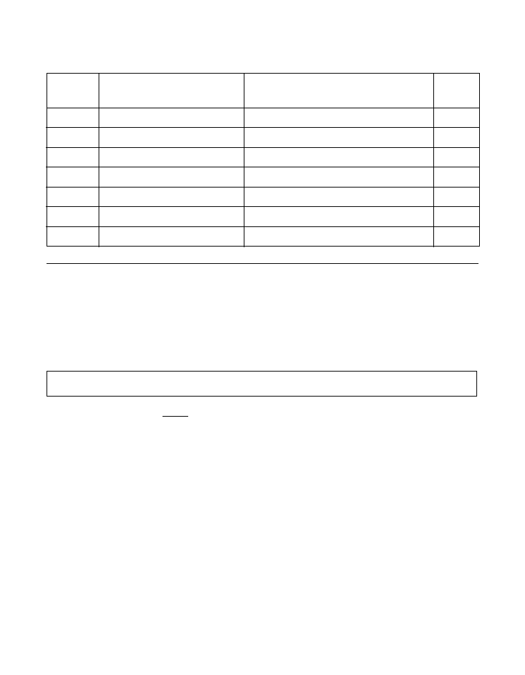
Register Definitions
4-11
Copyright � 2000�2001 by LSI Logic Corporation. All rights reserved.
4.3 Register Definitions
The following paragraphs describe the 8101/8104 internal registers.
4.3.1 Register 0�MAC Address 1
Note:
A[47] 15-bit occurs on the REGD15 pin.
A[47:32]
MAC Address, First Word
[15:0], R/W
This is the fist of three words in the 48-bit MAC address.
The MAC address is used to receive unicast address
filtering of the DA, and serves as the SA for automatically
generated MAC control pause frames.
A0 (see Register 2) corresponds to the first bit
transmitted or received by the MAC section (DA[0] or
SA[0] in
Figure 2.3
).
33�111
0b00011001�0b01101111
Reserved
112�115
0b01110000�0b01110011
Counter Half Full 1
-
4
0x0000
116�119
0b01110100�0b01110111
Reserved
120�123
0b01111000�0b01111011
Counter Half Full Mask 1�4
oxFFFF
124�127
0b01111100�0b01111111
Reserved
128�233
0b10000000�0b11101001
Counter 1-53 32-bit Management Counters 0x0000
234�255
0b11101010�0b11111111
Reserved
Table 4.3
Register Default Values (Cont.)
Register
Numbers
Register Address
(REGAD[7:0] Pins)
Register Name
Default
(Hex)
15
0
A[47:32]

4-12
Registers
Copyright � 2000�2001 by LSI Logic Corporation. All rights reserved.
4.3.2 Register 1�MAC Address 2
Note:
A[31] 15-bit occurs on the REGD15 pin.
A[31:16]
MAC Address, Second Word
[15:0], R/W
This is the second of three words in the 48-bit MAC
address.
The MAC address is used to receive unicast address
filtering of the DA, and serves as the SA for automatically
generated MAC control pause frames.
A0 (see Register 2) corresponds to the first bit
transmitted or received by the MAC section (DA[0] or
SA[0] in
Figure 2.3
.
4.3.3 Register 2�MAC Address 3
Note:
A[15] 15-bit occurs on the REGD15 pin.
A[15:0]
MAC Address, Third Word
[15:0], R/W
This is the third of three words that comprise the 48-bit
MAC address.
The MAC address is used to receive unicast address
filtering of the DA, and serves as the SA for automatically
generated MAC control pause frames.
A0 corresponds to the first bit transmitted or received by
the MAC section (DA[0] or SA[0] in
Figure 2.3
).
4.3.4 Register 3�MAC Address Filter 1
15
0
A[31:16]
15
0
A[15:0]
15
8
F7[7:0]

Register Definitions
4-13
Copyright � 2000�2001 by LSI Logic Corporation. All rights reserved.
Note:
F7[7] 15-bit occurs on the REGD15 pin.
F7[7:0], F6[7:0]
MAC Address Filter
[15:0], R/W
This is the first of four words in the 64-bit MAC address
filter.
The MAC address filter is used to filter the destination
address on multicast packets.
4.3.5 Register 4�MAC Address Filter 2
Note:
F5[7] 15-bit occurs on the REGD15 pin.
F5[7:0], F4[7:0]
MAC Address Filter
[15:0], R/W
This is the second of four words in the 64-bit MAC
address filter.
The MAC address filter is used to filter the destination
address on multicast packets.
7
0
F6[7:0]
15
8
F5[7:0]
7
0
F4[7:0]

4-14
Registers
Copyright � 2000�2001 by LSI Logic Corporation. All rights reserved.
4.3.6 Register 5�MAC Address Filter 3
Note:
F3[7] 15-bit occurs on the REGD15 pin
F3[7:0], F2[7:0]
MAC Address Filter
[15:0], R/W
This is the third of four words in the 64-bit MAC address
filter.
The MAC address filter is used to filter the destination
address on multicast packets.
4.3.7 Register 6�MAC Address Filter 4
Note:
F1[7] 15-bit occurs on the REGD15 pin
F1[7:0], F0[7:0]
MAC Address Filter
[15:0], R/W
This is the fourth of four words in the 64-bit MAC address
filter.
The MAC address filter is used to filter the destination
address on multicast packets.
15
8
F3[7:0]
7
0
F2[7:0]
15
8
F1[7:0]
7
0
F0[7:0]

Register Definitions
4-15
Copyright � 2000�2001 by LSI Logic Corporation. All rights reserved.
4.3.8 Register 7�Configuration 1
Note:
RST 15-bit occurs on the REGD15 pin
RST
Reset
15, R/WSC
RXRST
Receive Reset
14, R/WSC
TXRST
Transmit Reset
13, R/WSC
ANRST
AutoNegotiation Restart
12, R/WSC
CTRRST
Counter Reset
11, R/WSC
15
14
13
12
11
10
9
8
RST
RXRST
TXRST
ANRST
CTRRST
APAD
IPG[2:1]
7
6
5
4
3
2
1
0
IPG[0]
TXPRMBL
TXCRC
RXPRMBL
RXCRC
STSWRD1
STSWRD0
PEOF
RST
Description
1
Controller is reset; it self-clears in 1
�
s
0
Nominal operation
RXRST
Description
1
Receive data path reset, self-clears when the start
of the new packet is detected
0
Normal
TXRST
Description
1
Transmit data, data reset, self-clearing in 1
�
s
0
Normal
ANRST
Description
1
AutoNegotiation algorithm restarted, self-clearing
after AutoNegotiation process starts
0
No Reset
CTRRST
Description
1
All counters reset to 0, self-clearing in 1
�
s
0
No reset

4-16
Registers
Copyright � 2000�2001 by LSI Logic Corporation. All rights reserved.
APAD
AutoPad Enable
10, R/W
IPG[2:0]
Transmit Interpacket Gap Select
[9:7], R/W
TXPRMBL
Transmit Preamble Enable
6, R/W
TXCRC
Transmit CRC Enable
5, R/W
RXPRMBL
Receive Preamble Enable
4, R/W
APAD
Description
1
All undersize transmit packets padded to 64 bytes
0
No autopad
IPG[2:0]
Description
111
Tranmsit IPG is 96 bits (IEEE specification
minimum)
110
Transmit IPG is 122 bits
101
Transmit IPG is 80 bits
100
Transmit IPG is 64 bits
011
Transmit IPG is 192 bits-(2 x IEEE specification
minimum)
010
Transmit IPG is 384 bits-(4 x IEEE specification
minimum)
001
Transmit IPG is 768 bits-(8 x IEEE specification
minimum)
000
Transmit IPG is 32 bits
TXPRMBL
Description
1
Preamble added to beginning of transmit packet
0
Preamble not added
TXCRC
Description
1
CRC calculated and added to end of transmit
packet
0
CRC not added
RXPRMBL
Description
1
Preamble is stored in RX FIFO with rest of packet
0
Preamble stripped off

Register Definitions
4-17
Copyright � 2000�2001 by LSI Logic Corporation. All rights reserved.
RXCRC
Receive CRC Enable
3, R/W
STSWRD[1:0] Receive Status Word Append Select
[2:1], R/W
PEOF
Receive EOF Position Select
0, R/W
4.3.9 Register 8�Configuration 2
Note:
REJUCST 15-bit occurs on the REGD15 pin
REJUCST
Receive Unicast Packets Reject
15, R/W
RXCRC
Description
1
CRC is stored in RX FIFO with rest of packet
0
CRC stripped off
STSWRD[1:0]
Description
11
Reserved
10
Receive status word for nondiscarded packets
and discarded packets
01
Receive status word for nondiscarded packets
00
No receive status word
PEOF
Description
1
Receive EOF at end of packet data
0
Receive EOF at end of receive status word
15
14
13
12
11
10
9
8
REJUCST
REJMCST
REJBCST
REJALL
ACPTALL
DIS_OVF
DIS_CRC
DIS_USIZE
7
6
5
4
0
DIS_OSIZE
DIS_CWRD
DIS_RXAB
RES = 0
REJUCST Description
1
Receiver rejects all unicast packets
0
Accept unicast packet if DA value in registers [0:2]

4-18
Registers
Copyright � 2000�2001 by LSI Logic Corporation. All rights reserved.
REJMCST
Receive Multicast Packets Reject
14, R/W
REJBCST
Receive Broadcast Packets Reject
13, R/W
REJALL
Receive All Packet Reject
12, R/W
ACPTALL
Receive All Packets Enable
11, R/W
DIS_OVF
Discard Overflow Packet Enable
10, R/W
DIS_CRC
Discard CRC Error Packet Enable
9, R/W
REJMCST
Description
1
Receiver rejects all multicast packets
0
Accept multicast packet if DA passes MAC
address filter
REJBCST
Description
1
Receiver rejects all broadcast packets
0
Accept broadcast packet
REJALL
Description
1
Receiver rejects all packets
0
Normal
ACPTALL
Description
1
Receiver accepts all packets regardless of
address (not including MAC control frames)
0
Normal
DIS_OVF
Description
1
Discard receive packet with receive FIFO
overflow error
0
No discard
DIS_CRC
Description
1
Discard receive packet with CRC error
0
No discard

Register Definitions
4-19
Copyright � 2000�2001 by LSI Logic Corporation. All rights reserved.
DIS_USIZE
Discard Undersize Packet Enable
8, R/W
DIS_OSIZE
Discard Oversize Packet Enable
7, R/W
Note:
Clearing this bit to 0 allows maximum packet size to be
unlimited in length.
DIS_CWRD
Discard Codeword Error Packet Enable
6, R/W
DIS_RXAB
Discard RXABORT Packet Enable
5, R/W
RES
Reserved
[4:0], R/W
Must be left at default value or written to 0 for proper
operation.
4.3.10 Register 9�Configuration 3
Note:
RES 15-bit occurs on the REGD15 pin
DIS_USIZE
Description
1
Discard receive undersize packet
0
No discard
DIS_OSIZE
Description
1
Discard receive oversize packet
0
No discard
DIS_CWRD
Description
1
Discard receive packets that contain PCS
codeword error
0
No discard
DIS_RXAB
Description
1
Discard receive packets that are aborted with
RXABORT
0
No discard (i.e. RXABORT pin is disabled)
15
14
13
12
11
10
9
8
RES
AUTOCLR
AUTORXAB
CTR_RD
CTR_ROLL
EWRAP
LCKREF
7
6
5
4
3
2
1
0
CDET
AN_EN
RMXPKT1
RMXPKT2
RXAB_DEF
SINTF_DIS FCNTRL_DIS
SD_EN

4-20
Registers
Copyright � 2000�2001 by LSI Logic Corporation. All rights reserved.
RES
Reserved
[15:14]
,
R/W
Must be left at default value or written to 0 for proper
operation.
AUTOCLR
AutoClear Mode Enable
13, R/W
AUTORXAB
AutoAbort Enable
12, R/W
CTR_RD
Counter Reset On Read Enable
11, R/W
CTR_ROLL
Counter Rollover Enable
10, R/W
EWRAP
EWRAP Pin Assert
9, R/W
LCKREF
LCKREFn Pin Assert
8, R/W
AUTOCLR
Description
1
TXDC and RXDC automatically cleared at next
EOF
0
TXDC and RXDC cleared by CLR_TXDC and
CLR_RXDC pins, respectively
AUTORXAB
Description
1
Current packet aborted and RXDC automatically
cleared at next EOF
0
No Abort
CTR_RD
Description
1
Counters reset to 0 when read
0
Counters not reset when read (only if count
<
maximum count)
CTR_ROLL
Description
1
Counters rollover to 0 after maximum count
0
Counters stop at maximum count
EWRAP
Description
1
EWRAP pin is asserted active HIGH
0
Deassert
LCKREF
Description
1
LCKREFn pin is asserted
0
Deassert

Register Definitions
4-21
Copyright � 2000�2001 by LSI Logic Corporation. All rights reserved.
CDET
EN_CEDT Pin Assert
7, R/W
AN_EN
AutoNegotiation Enable
6, R/W
RMXPKT[1:0] Receive MAC Maximum Packet Size Select
[5:4], R/W
Note:
Max packet size is unlimited if bit 7 = 0
RXAB_DEF
RXABORT Pin Definition
3, R/W
SINTF_DIS
System Interface Disable
2, R/W
CDET
Description
1
EN_CDET pin is asserted active HIGH
0
EN_CDET pin is controlled by receive PCS
state machine
AN_EN
Description
1
AutoNegotiation algorithm enabled
0
Disabled
RMXPKT[1:0]
Description
11
Reserved
10
1535 Bytes
01
1522 Bytes
00
1518 Bytes
RXAB_DEF
Description
1
RXABORT pin and autoabort feature discards
data
0
RXABORT pin and autoabort feature discards
data and status word
SINTF_DIS
Description
1
System interface disabled (see system
interface section)
0
Normal

4-22
Registers
Copyright � 2000�2001 by LSI Logic Corporation. All rights reserved.
FCNTRL_DIS FCNTRL Pin
1, R/W
SD_EN
Signal Detect Pin Enable
0, R/W
4.3.11 Register 10�Configuration 4
Note:
ENDIAN 15-bit occurs on the REGD15 pin
ENDIAN
Endian Select
15, R/W
BUSSIZE
Bus Size Word Width
14, R/W
RES
Reserved
13, [9:8], [5:0], R/W
Must be left at default value or written to 0 for proper
device operation.
LPBK
Loopback Enable
12, R/W
FCNTRL_DIS Description
1
FCNTRL pin disabled (does not cause
autogenerated pause frame transmission).
0
Enabled
SD_EN
Description
1
Enabled
0
SD pin disabled, i.e., internal SD always asserted,
does not affect receive word synchronization
15
14
13
12
11
10
9
8
7
6
5
0
ENDIAN BUSSIZE
RES
LPBK
LNKDN
TBC_DIS
RES
CMXPKT1 CMXPKT0
RES
ENDIAN
Description
1
RXD/TXD data in big endian format
0
RXD/TXD data in little endian format
BUSSIZE
Description
1
Receive system bus word width is 16 bits
0
Receive system bus word width is 32 bits
LPBK
Description
1
Loopback mode enabled
0
Normal

Register Definitions
4-23
Copyright � 2000�2001 by LSI Logic Corporation. All rights reserved.
LNKDN
Link Down FIFO Flush Enable
11, R/W
TBC_DIS
TX Disable
10, R/W
RES
Reserved
[9:8], [5:0] R/W
Must be left at default value or written to 0 for proper
device operation.
CMXPKT[1:0] Counter Max Packet Size Select
[7:6], R/W
4.3.12 Register 11�Status 1
Note:
RSYNC 15-bit occurs on the REGD15 pin
RSYNC
Receive Word Synchronization Detect
15, R/LTI
RES
Reserved
[14:13], [10:8], [2:0]
Must be left at default value or written to 0 for proper
device operation.
LNKDN
Description
1
When receive link is down, data exiting the TX
FIFO is discarded
0
Normal
TBC_DIS
Description
1
TBC, TX [9:0] outputs disabled (high impedance)
0
Enabled
CMXPKT[1:0]
Description
11
Unlimited
10
1535 bytes
01
1522 bytes
00
1518 bytes
15
14
13
12
11
10
8
7
6
5
4
3
2
0
RSYNC
RES
SD
LINK
RES
AN_NP AN_TX_NP AN_RX_NP AN_RX_BP AN_RMTRST
RES
RSYNC
Description
1
Receive 8B10B PCS has acquired word
synchronization
0
Not synchronized

4-24
Registers
Copyright � 2000�2001 by LSI Logic Corporation. All rights reserved.
SD
Signal Detect Pin Status
12, R
LINK
Link Detect Status
11, R/LTI
AN_NP
AutoNegotiation Next Page Status
7, R/LHI
AN_TX_NP
AutoNegotiation TX Next Page Status
6, R
AN_RX_NP
AutoNegotiation RX Next Page Status
5, R
AN_RX_BP
AutoNegotiation RX Base Page Status
4, R
AN_RMTRST AutoNegotiation Remote Restart Status
3, R/LHI
SD
Description
1
SD input pin HIGH
0
SD input pin LOW
LINK
Description
1
Link pass (receiver in sync, AutoNegotiation done)
0
Link fail
AN_NP
Description
1
One next page exchange done (both RX and TX)
0
Not done
AN_TX_NP
Description
1
Transmission of next page done
0
Not done
AN_RX_NP
Description
1
Reception of next page done, next page valid
0
Not done
AN_RX_BP
Description
1
Reception of base page done, base page valid
0
Not done
AN_RMTRST
Description
1
AutoNegotiation restarted because remote
end sent restart codes or invalid characters
0
Normal

Register Definitions
4-25
Copyright � 2000�2001 by LSI Logic Corporation. All rights reserved.
4.3.13 Register 14�Status Mask 1
Note:
MASK_RSYNC 15-bit occurs on the REGD15 pin
MASK_RSYNC
Interrupt Mask - Receive Word Synchronization
Detect
15, R/W
RES
Reserved
[14:12], [10:8], [6:4], [2:0], R/W
Must be left at default value or written to 1 for proper
device operation.
MASK_LINK
Interrupt Mask - Link Status Detect
11, R/W
MASK_AN_NP
Interrupt Mask - AutoNegotiation Next Page
Status
7, R/W
MASK_AN_RMTRST
Interrupt Mask - AutoNegotiation Remote Restart
Status
3, R/W
15
14
12
11
10
8
7
6
4
3
2
0
MASK_RSYNC RES = 1 MASK_LINK RES = 1
MASK_AN_NP
RES = 1
MASK_AN_RMTRST
RES = 1
MASK_RSYNC
Description
1
Mask interrupt for RSYNC in Register 11
0
No mask
MASK_LINK
Description
1
Mask interrupt for LINK in Register 11
0
No mask
MASK_AN_NP
Description
1
Mask interrupt for AN_NP in Register 11
0
No mask
MASK_AN_RMTRST
Description
1
Mask interrupt for AN_RMTRST in
Register 11
0
No mask

4-26
Registers
Copyright � 2000�2001 by LSI Logic Corporation. All rights reserved.
4.3.14 Register 17�Transmit FIFO Threshold
Note:
TWM1[4] 15-bit occurs on the REGD15 pin
TWM1[4:0]
Transmit FIFO Watermark 1 Threshold
[15:11], R/W
TWM2[4:0]
Transmit FIFO Watermark 2 Threshold
[10:6], R/W
15
11
10
6
5
0
TWM1[4:0]
TWM2[4:0]
TASND[5:0]
TWM1[4:0]
Description
Range
0
-
1024 words (0
-
4096 bytes)
Increment
32 words (128 bytes)
11111
Reserved, do not use
11110
992 words in FIFO (3968 bytes)
11101
960 words in FIFO (3840 bytes
00001
64 words in FIFO (256 bytes)
00000
32 words in FIFO (128 bytes)
.
..
TWM2[4:0]
Description
Range
0
-
1024 words (0
-
4096 bytes)
Increment
32 words (128 bytes)
11111
Reserved, do not use
11110
992 words in FIFO (3968 bytes)
11101
960 words in FIFO (3840 bytes)
00001
64 words in FIFO (256 bytes)
00000
32 words in FIFO (128 bytes)
.
..

Register Definitions
4-27
Copyright � 2000�2001 by LSI Logic Corporation. All rights reserved.
TASND[5:0]
Transmit FIFO AutoSend Threshold
[5:0], R/W
Note 1:
An EOF written into FIFO also starts transmission of that
packet regardless of the AutoSend threshold setting.
Note 2:
The 0b000000 setting in TASND[5:0] lets the FIFO fill up
before transmission starts, facilitating transmission of
oversize packets.
4.3.15 Register 18�Receive FIFO Threshold
Note:
RWM1[15] 15-bit occurs on REGD15 pin.
RWM1[7:0]
Receive FIFO Watermark 1 Threshold
[15:8], R/W
TASND[5:0]
Description
Range
0
-
1024 words (0
-
4096 bytes)
Increment
8 words (32 bytes)
111111
Reserved do not use
111110
Transmit starts when 504 words in FIFO
000010
Transmit starts when 24 words in FIFO
000001
Transmit starts when 16 words in FIFO
000000
Transmit starts when 992 words in FIFO
.
..
15
8
7
0
RWM1[7:0]
RWM2[7:0]
RWM1[7:0]
Description
Range
0
-
4096 words (0
-
16386 bytes)
Increment
16 words (64 bytes)
11111111
Reserved, do not use
11111110
4080 words in FIFO (16320 bytes)
11111110
4064 words in FIFO (16256 bytes)
00000001
32 words in FIFO (128 bytes)
00000000
16 words in FIFO (64 bytes)
.
..

4-28
Registers
Copyright � 2000�2001 by LSI Logic Corporation. All rights reserved.
RWM2[7:0]
Receive FIFO Increment = 16 Words (64 Bytes)
Watermark 2 Threshold
[7:0], R/W
4.3.16 Register 19�Flow Control 1
Note:
MCNTRL 15-bit occurs on REGD15 pin
MCNTRL
MAC Control Frame Enable
15, R/W
MCPASS[1:0]
MAC Control Frame Pass Through
Enable
[14:13], R/W
RWM2[7:0]
Description
Range
0
-
4096 words (0
-
16386 bytes)
11111111
Reserved, do not use
11111110
4080 words in FIFO (16320 bytes)
11111110
4064 words in FIFO (16256 bytes)
00000001
32 words in FIFO (128 bytes)
00000000
16 words in FIFO (64 bytes)
.
..
15
14
13
12
11
10
7
6
0
MCNTRL
MCPASS[1:0]
MCFLTR
MCENDPS
MCASND[3:0]
RES = 0
MCNTRL
Description
1
Valid receive MAC control frames cause the
transmitter to pause (flow control enabled)
0
Transmitter not paused (flow control disable)
MCPASS[1:0] Description
11
Valid MAC control frame that have pause
opcode are passed through to receive FIFO
10
Valid MAC control frames that have any opcode
are passed through to receive FIFO
01
Valid MAC control frames that have nonpause
opcode are passed through to receive FIFO
00
MAC control frames are not passed through to
receive FIFO

Register Definitions
4-29
Copyright � 2000�2001 by LSI Logic Corporation. All rights reserved.
MCFLTR
MAC Control Frame Address Filter Enable
12, R/W
MCENDPS
MAC Control Frame End Pause Enable
11, R/W
MCASND[3:0]
MAC Control Frame AutoSend
Threshold
[10:7], R/W
These bits determine the receive FIFO threshold, which
causes the automatic transmission of pause frames.
Autogenerated pause frame transmission is also affected
by the FCNTRL pin and bit 1.
RES
Reserved
[6:0], R/W
Must be left at defaults or written to 0 for proper
operation.
4.3.17 Register 20�Flow Control 2
Note:
P15 15-bit occurs on REGD15 pin
MCFLTR
Description
1
Use reserved multicast address or station
address as the DA to determine MAC control
pause frame validity
0
Use any address as the DA to determine MAC
control pause frame validity
MCENDPS
Description
1
When FNCTRL is deasserted, send transmit
MAC control frame with pause_time = 0
0
Normal
MCASND[3:0]
Description
1111
15360 bytes
0010
2048 bytes
0001
1024 bytes
0000
Disabled, i.e. RX FIFO data does not cause
autogenerated pause frame transmission.
.
..
15
0
P[15:0]

4-30
Registers
Copyright � 2000�2001 by LSI Logic Corporation. All rights reserved.
P[15:0]
Pause Time
[15:0], R/W
The contents of this register are inserted into the
pause_time parameter field of all autogenerated transmit
MAC control pause frames. Upon successful reception of
these autogenerated pause frames, a remote device
does not transmit data for a time interval equal to the
decimal value of this register times 512 ns.
P0 is the LSB.
Any pause time value less than or equal to 0x32 is sent
as 0x32.
4.3.18 Register 21�AutoNegotiation Base Page Transmit
Note:
NP 15-bit occurs on REGD15 pin
NP
Next Page Enable
15, R/W
ACK
Acknowledge
14, R/W
Note
:
Writing this bit has no effect on device operation. The
transmitted bit is controlled by internal state machine.
RF[2:1]
Remote Fault
[13:12], R/W
15
14
13
12
11
9
8
7
6
5
4
0
NP
ACK
RF[2:1]
RES
PS_DIR
PS
HDX
FDX
RES
NP
Description
1
Next page exists
0
No next page
ACK
Description
1
Received AutoNegotiation word recognized
0
Not recognized
RF[2:1]
Description
11
AutoNegotiation error
10
Offline
01
Link failure
00
No error, link OK

Register Definitions
4-31
Copyright � 2000�2001 by LSI Logic Corporation. All rights reserved.
RES
Reserved
[11:9], R/W
Reserved for future IEEE use
PS_DIR PS
Pause Capable
[8:7], R/W
HDX
Half-Duplex Capable
6, R/W
FDX
Full-Duplex Capable
5, R/W
RES
Reserved
[4:0], R/W
Reserved for future IEEE use.
4.3.19 Register 22�AutoNegotiation Base Page Receive
Note:
NP 15-bit occurs on the REGD15 pin.
NP
Next Page Enable
15, R
PS_DIR PS
Description
11
Capable of receive pause only
10
Capable of transmit pause only
01
Capable of transmit and receive pause
00
Not capable
HDX
Description
1
Capable of half duplex
0
Not capable
FDX
Description
1
Capable of full duplex
0
Not capable
15
14
13
12
11
9
8
7
6
5
4
0
NP
ACK
RF[2:1]
RES
PS_DIR
PS
HDX
FDX
RES
NP
Description
1
Next page exists
0
No next page

4-32
Registers
Copyright � 2000�2001 by LSI Logic Corporation. All rights reserved.
ACK
Acknowledge
14, R
RF[2:1]
Remote Fault
[13:12], R
RES
Reserved
[11:9], [4:0], R
Reserved for future IEEE use.
PS_DIR, PS
Pause Capable
[8:7], R
HDX
Half-Duplex Capable
6, R
FDX
Full-Duplex Capable
5, R
ACK
Description
1
Received AutoNegotiation word recognized
0
Not recognized
RF[2:1]
Description
11
AutoNegotiation error
10
Offline
01
Link failure
00
No error, link OK
PS_DIR, PS
Description
11
Capable of receive pause only
10
Capable of transmit pause only
01
Capable of transmit and receive pause only
00
Not capable
HDX
Description
1
Capable of half-duplex
0
Not capable
FDX
Description
1
Capable of full-duplex
0
Not capable

Register Definitions
4-33
Copyright � 2000�2001 by LSI Logic Corporation. All rights reserved.
4.3.20 Register 23�AutoNegotiation Next Page Transmit
Note:
NP 15-bit occurs on REGD15 pin
NP
Next Page Enable
15, R/W
ACK
Acknowledge
14, R/W
Note:
Writing this bit has no effect on device operation. The
transmitted bit is controlled by internal state machine.
PAGE
Page Type
13, R/W
ACK2
Acknowledge 2
12, R/W
15
14
13
12
11
10
0
NP
ACK
PAGETYPE
ACK2
TOGGLE
MSG[10:0]
NP
Description
1
Additional next page exists
0
This is the last next page
ACK
Description
1
Received AutoNegotiation word recognized
0
Not recognized
PAGE
Description
1
Message page
0
Unformatted page
ACK2
Description
1
Able to comply with the received message
0
Not able to comply

4-34
Registers
Copyright � 2000�2001 by LSI Logic Corporation. All rights reserved.
TOGGLE
Toggle Bit
11, R/W
Note:
Writing this bit has no effect on device operation. The
transmitted bit is controlled by internal state machine.
MSG[10:0]
Message
[10:0], R/W
These bits carry the 11-bit message associated with this
next page. Refer to IEEE 802.3z specifications for details
on the format and definition of these bits.
4.3.21 Register 24�AutoNegotiation Next Page Receive
Note:
NP 15-bit occurs on the REGD15 pin
NP
Next Page Enable
15, R
ACK
Acknowledge
14, R
PAGETYPE
Page Type
13, R
TOGGLE
Description
1
Value of the toggle bit in previously transmitted
AutoNegotiation word was 0
0
Value of the toggle bit in previously transmitted
AutoNegotiation word was 1
15
14
13
12
11
10
0
NP
ACK
PAGETYPE
ACK2
TOGGLE
MSG[10:0]
NP
Description
1
Additional next page exists
0
This is last next page
ACK
Description
1
Received AutoNegotiation word recognized
0
Not recognized
PAGETYPE
Description
1
Message page
0
Unformatted page

Register Definitions
4-35
Copyright � 2000�2001 by LSI Logic Corporation. All rights reserved.
ACK2
Acknowledge 2
12, R
TOGGLE
Toggle Bit
11, R
MSG[10:0]
Message
[10:0], R
These bits carry the 11-bit message associated with this
next page. Refer to the IEEE 802.3z specifications for
details on the format and definition of these bits.
4.3.22 Register 32�Device ID
Note:
PART[3] 15-bit occurs on the REGD15 pin.
PART[3:0]
Part Number
[15:12], R
This field contains a 4-bit number that uniquely identifies
the device.
HREV[3:0]
Hardware Revision Number
[11:8], R
This field contains a 4-bit number that identifies that a
revision was made to the device and the revision did not
affect any register bit definitions.
RES
Reserved
[7:4], R/W
Reserved for future use.
SREV[3:0]
Software Revision Number
[3:0], R/W
This field contains a 4-bit number that identifies that a
revision was made to the device and the revision did
affect register bit definitions.
ACK2
Description
1
Able to comply with the received message
0
Not able to comply
TOGGLE
Description
1
Value of the toggle bit in previous transmitted
AutoNegotiation word was 0
0
Value of the toggle bit in previous transmitted
AutoNegotiation word was 1
15
12
11
8
7
4
3
0
PART[3:0]
HREV[3:0]
RES
SREV[3:0]

4-36
Registers
Copyright � 2000�2001 by LSI Logic Corporation. All rights reserved.
4.3.23 Register 112�115�Counter Half Full 1
-
4
Note:
HFULL[15] 15-bit occurs on the REGD15 pin.
HFULL[15:0]
Counter Half Full Detect
[15:0], R/LHI
These bits indicate when a counter is near overflow is
half full. These four registers contain 53 counter half-full
detect bits, one bit for each of the 53 counters.
Bit 0 in Counter Half Full Register 0 corresponds to
Counter 1 as listed in
Table 4.1
; bit 15 in Counter Half
Full Register 0 corresponds to Counter 16; bit 4 of
Counter Half Full Register 4 corresponds to Counter 53.
4.3.24 Registers 120�123�Counter Half Full Mask 1
-
4
Note:
MASK_HFULL[15] 15-bit occurs on the REGD15 pin
MASK_HFULL[15:0]
Counter Half Full Detect Mask
[15:0], R/W
The MASK_HFULL[15:0] bits mask (disable) the interrupt
caused by the counter half-full detect bits. These four
registers contain 53 mask bits, one bit for each of the 53
half-full detect bits.
Bit 0 in Counter Half Full Mask Register 0 masks the
interrupt caused by the half full detect bit for Counter 1;
bit 15 in Counter Half Full Mask Register 0 corresponds
to Counter 16; bit 4 in Counter Half Full Mask Register 3
corresponds to Counter 53.
15
0
HFULL[15:0]
HFULL[15:0]
Description
1
Counter has reached a count of 0x80000000,
(half full).
0
Count
<
0x80000000
15
0
MASK_HFULL[15:0]

Register Definitions
4-37
Copyright � 2000�2001 by LSI Logic Corporation. All rights reserved.
4.3.25 Registers 128
-
233�Counter 1
-
53
Note:
C15 15-bit occurs on the REGD15 pin.
C[15:0]
Counter Result Value
[15:0], R
These 106 registers contain the results of the 53 32-bit
management counters.
Each 32-bit counter result value resides in two 16-bit
registers. For the two registers associated with each
counter, the register with the lower value address always
contains the least-significant 16 bits of the counter result.
C0 of the lower value address is the counter LSB; C15 of
the higher value is the counter MSB.
The definition and register address for each counter is
shown in
Table 2.14
. The register address for each
counter is also shown in
Table 4.2
.
MASK_HFULL[15:0] Description
1
Mask (disable) the interrupt caused by
the corresponding Counter Half Full
Detect Bit.
0
No mask
15
0
C[15:0]

4-38
Registers
Copyright � 2000�2001 by LSI Logic Corporation. All rights reserved.

8101/8104 Gigabit Ethernet Controller
5-1
Copyright � 2000�2001 by LSI Logic Corporation. All rights reserved.
Chapter 5
Application Information
This Chapter provides application information for the 8101/8104 Gigabit
Ethernet Controller. The chapter contains the following sections
�
Section 5.1, "Typical Ethernet Port"
�
Section 5.2, "10-Bit PHY Interface"
�
Section 5.3, "System Interface"
�
Section 5.4, "Reset"
�
Section 5.5, "Loopback"
�
Section 5.6, "AutoNegotiation"
�
Section 5.7, "Management Counters"
�
Section 5.8, "TX Packet and Octet Counters"
�
Section 5.9, "Power Supply Decoupling"

5-2
Application Information
Copyright � 2000�2001 by LSI Logic Corporation. All rights reserved.
5.1 Typical Ethernet Port
A typical example of a Gigabit Ethernet switch port using the 8101/8104
controller is shown in
Figure 5.1
.
Figure 5.1
Gigabit Ethernet Switch Port Using the 8101/8104
5.2 10-Bit PHY Interface
The 10-bit PHY interface directly couples to any external physical layer
device that complies with the IEEE 802.3z or the 10-bit ANSI X3.230
interface standards.
5.2.1 External Physical Layer Devices
In a typical configuration, the controller is connected to an external
Serializer/Deserializer (SerDes) Integrated circuit, as shown in
Figure 5.1
. A list of SerDes devices whose specifications are compatible
with and can directly connect to the controller is shown in
Table 5.1
.
TX DATA
RX DATA
MGMT
8101/8104
Gigabit
MAC + PCS
32
32
16
IEEE
802.3 10-Bit
Interface
Serializer/
Deserializer
IC
ANSI
PECL
Interface
Fiber
Optic
Transceiver
Optical
Fiber
MAC
PHY

System Interface
5-3
Copyright � 2000�2001 by LSI Logic Corporation. All rights reserved.
5.2.2 Printed Circuit Board Layout
The 10-bit PHY interface clocks data at 125 MHz. The setup and hold
times on the timing signals are very short. The outputs are specified
assuming a maximum load of only 10 pf. For these reasons, it is
imperative that the SerDes or other physical layer device be placed as
close as possible to the controller, preferably within one inch. In addition,
care should be taken to eliminate any extra loading on all the 10-bit PHY
interface signal lines. Also, the clock and data lines in both receive and
transmit directions should be routed along the same paths so that they
have similar parasitics and delays, to prevent degrading setup and hold
times. Termination is not necessary if these precautions are taken.
5.3 System Interface
The system interface requires the selection of watermarks and close
attention to printed circuit board layout.
5.3.1 Watermarks
There are two independent watermarks on both the transmit and receive
FIFOs. The usage of these watermarks is unspecified and is left to the
discretion of the system designer. Below are three examples of
watermark usage based on transferring data in any of the following ways:
�
Complete packets
�
Fixed block sizes
�
Variable block sizes
Table 5.1
Compatible SerDes Devices
Vendor
Device No.
Vitesse
VSC7135
Hewlett-Packard
HDMP-1636
HDMP-1646
Sony
CXB1589Q
AMCC
52052
TriQuint
TQ9506

5-4
Application Information
Copyright � 2000�2001 by LSI Logic Corporation. All rights reserved.
5.3.1.1 Complete Packet Watermarks
To transfer data to and from the controller in completed packets, only one
watermark is needed. Either transmit watermark could be chosen for this
application. On the receive side, RXWM2 should be chosen because it
is asserted when a complete packet is loaded into the RX FIFO. The
transmit and receive watermark thresholds should preferably be set to a
value equal to or larger than the maximum size packet (1518 bytes or
greater). On the transmit side, the data is written into the TX FIFO in
complete packet bursts when the system requires. On the receive side
the data is read out of the RX FIFO beginning with the assertion of
RXWM2 and ending when RXEOF is asserted.
5.3.1.2 Fixed Block Watermarks
To transfer data to and from the controller in fixed block sizes (64 bytes
at a time, for example), only one watermark is needed. Either transmit
watermark could be chosen for this application. On the receive side,
RXWM2 should be chosen because it is asserted when a complete
packet is loaded into the RX FIFO. The transmit watermark threshold is
set to a low value (64 bytes for example), and the receive watermark
thresholds preferably are set to a value equal to or greater than the fixed
cell size (64 bytes in this example). On the transmit side, the data is
written into the TX FIFO in fixed block size bursts when the system
requires. When the transmit watermark is deasserted, another block
must be written into the TX FIFO. On the receive side, the data is read
out of the RX FIFO beginning with the assertion of RXWM2 and ending
when the fixed block has been read out (64 bytes in this example) or
RXEOF has been asserted.
5.3.1.3 Variable Block Watermarks
To transfer data to and from the controller in variable cell sizes, two
watermarks are needed. The TXWM1n and RXWM1 watermark
thresholds are set to some low value (64 bytes for this example) while
the TXWM2n and RXWM2 watermark thresholds are set to some high
value (1024 bytes for example). On the transmit side, the data is written
into the TX FIFO when the system requires. If TXWM2n is asserted, the
data input must be halted. If TXWM1n is deasserted, the data input must
be resumed. In this way, the TX FIFO contents are kept between the high
and low watermark thresholds, which potentially increses the external

Reset
5-5
Copyright � 2000�2001 by LSI Logic Corporation. All rights reserved.
system loading efficiency. Similarly, on the receive side the data must be
read out of the RX FIFO when RXWM2 is asserted. If RXWM1 is
deasserted, or RXEOF is asserted, the data output must be halted. If
RXWM2 is asserted the data output must be resumed. In this way, the
RX FIFO contents are kept between the high and low watermarks.
The transmit and receive watermarks can also be used to indicate that
the FIFO is full or empty (or almost full or almost empty), if desired.
5.3.2 PCB Layout
Because the data rate of the system interface can be as high as 66 MHz,
care should be taken to keep PCB trace lengths of all critical signals as
short as possible, preferably less than 2 inches in length. If this guideline
is followed termination is not necessary.
5.4 Reset
While the device is being reset, it transmits valid 10B symbols out of the
10-bit PHY interface on TXD[0:9] and TBC. If the device is reset with the
RESETn pin for a long period of time, these 10B symbols may be
mistakenly decoded as valid packet information and fill up the memory
in a remote device. The reset procedure outlined in
Table 5.2
avoids this
situation and is recommended for use when the RESETn pin is asserted
for long periods of time. When the reset bit is used for device reset the
above situation is avoided because the reset bit is self-clearing in 1
�
s.

5-6
Application Information
Copyright � 2000�2001 by LSI Logic Corporation. All rights reserved.
5.5 Loopback
The controller has a loopback mode, but most external SerDes devices
connected to the controller 10-bit PHY interface also have a loopback
mode. Sometimes it is desirable to use the SerDes loopback mode
instead of the controller loopback mode because the SerDes loopback
mode tests a larger and/or different section of the system circuitry. When
the SerDes loopback mode is used, it is recommended that the
procedure outlined in
Table 5.3
be followed.
Table 5.2
Reset Procedure
Step
Action
Result
1
Set the TBC_DIC bit
Stop transmission of data from the 10-bit PHY interface to
SerDes.
2
Wait for more than 20
�
s
Insures that the remote device receiver detects that the link has
been broken
so it will not decode 10B data as valid.
3
Assert RESETn
Start the reset period.
4
Wait more than 10
�
s.
Allow enough time for all circuits
in controller to be reset.
5
Deassert RESETn
Stop the reset period.
6
Clear the TBC_DIC bit
Turns on 10-bit PHY interface and returns controller to normal
operation.

AutoNegotiation
5-7
Copyright � 2000�2001 by LSI Logic Corporation. All rights reserved.
5.6 AutoNegotiation
AutoNegotiation is a handshake operation between the controller and the
external device (see
Section 2.15, "AutoNegotiation"
). If the external
device is capable of AutoNegotiation, the procedures described in
Section 5.6.1, "AutoNegotiation at Power Up"
should be followed. If the
external device is not capable of AutoNegotiation, refer to
Section 5.6.2,
"Negotiating with a Non-AutoNegotiation Capable Device"
.
Table 5.3
SerDes Loopback Procedure
STEP
Action
Result
1
Set the REJALL bit in Register 8 Ignore all receive data until the loopback mode is ready
for operation.
2
Set the EWRAP bit in Register 9 Enable the external SerDes loopback mode.
3
Clear the SD_EN bit in Register
9
Ignore the signal detect output from optical transceiver
because the receive optical data may be invalid.
4
Set the TBC_DIS bit in Register
10
Stop transmission of data out of 10-bit PHY interface
which causes the SerDes and controller to lose sync so
that they properly resync to the new data stream.
5
Wait more than 200
�
s
Allow time for the SerDes and controller receivers to lose
sync.
6
Clear the TBC_DIS bit in
Register 10
Turn on the transmitter so that the SerDes and controller
receivers can gain sync.
7
Wait more than 200
�
s
Allow time for the SerDes and controller receivers to gain
sync.
8
Clear the REJALL bit in Register
8
Stop ignoring receive data and turn on the receive MAC.
9
Do loopback tests
10
Clear the EWRAP bit, and set
the SD_EN bit in Register 9 (if
SD pin is used)
Turn off the SerDes loopback mode and enable the signal
detect function (if used).
11
Set the ANRST bit in Register 7 Restarts AutoNegotiation. Controller is ready for normal
operation when AutoNegotation is completed.

5-8
Application Information
Copyright � 2000�2001 by LSI Logic Corporation. All rights reserved.
5.6.1 AutoNegotiation at Power Up
When the device is powered up the AutoNegotiation algorithm must
handshake with the remote device to configure itself for a common mode
of operation. To insure smooth and proper AutoNegotiation operation at
power up it is recommended that the procedure outlined in
Table 5.4
be
followed.
Table 5.4
AutoNegotiation Power Up Procedure
STEP
Action
Result
1
Wait for the SD pin to go HIGH (If
SD is not used, go to the next step.)
Waits for valid data from the optical transceiver.
2
Set RST bit in Register 7
Resets the device.
3
Set bits [15:0] in Register 21
Sets up the capabilities for AutoNegotiation.
4
Set the remaining
register bits as needed.
Sets up the device for the desired operation.
5
Set ANRST bit in Register 7
Restarts AutoNegotiation.
6
Wait > 50
�
s
Wait for AutoNegotiation to complete.
7
Read LINK bit in register 11 twice. If
0, then done. If 1, repeat #5�7
(up to seven times).
Determine if AutoNegotiation done and link pass. If
link pass, device ready for operation. If link fail, retry
again seven more times. If no link pass after seven
times, disable ANEG and try manual link pass.
8
Clear AN_EN bit in Register 9
Disable AutoNegotiation.
9
Clear ANRST bit in Register 7
Clears all internal AutoNegotiation circuitry.
10
Wait > 100
�
s
Wait for manual link pass.
11
Read LINK bit in Register 11 twice.
If 0, go to first step. If 1, done.
If manual link pass, then device ready for operation. If
link fail, then redo procedure until link pass is
achieved.

Management Counters
5-9
Copyright � 2000�2001 by LSI Logic Corporation. All rights reserved.
5.6.2 Negotiating with a Non-AutoNegotiation Capable Device
When the controller has AutoNegotiation enabled and the remote device
to which it is connected has the AutoNegotiation disabled (or does not
have AutoNegotiation capability at all), the controller stays in the link fail
state and continually restarts AutoNegotiation because it cannot
complete a negotiation sequence successfully. Conversely, the remote
device goes to the link pass state because it sees the AutoNegotiation
words transmitted to it as valid idle symbols. For proper operation
between two devices, the controller and the remote device must both be
either set with AutoNegotiation enabled or set with AutoNegotiation
disabled.
5.7 Management Counters
The controller management counters provide the necessary statistics to
completely support the following IETF and IEEE specifications:
�
IETF RFC 1757:
RMON Statistics Group
�
IETF RFC 1213 and 1573
SNMP Interfaces Group
�
IETF RFC 1643:
Ethernet-Like MIB
�
IEEE 802.3/Cl. 30:
Ethernet MIB
A complete list of the counters along with their definitions was already
defined in
Table 2.14
. A map of the actual MIB objects from the IETF
and IEEE specifications to the specific controller counters is shown
below in
Table 5.5
�
Table 5.8
.

5-10
Application Information
Copyright � 2000�2001 by LSI Logic Corporation. All rights reserved.
Table 5.5
MIB Objects vs. Counter Location for RMON Statistics
Group MIB (RFC 1757)
Counter Location
MIB Objects
Counter
Register Address
(Low/High)
etherStatsDropEvents
1
0b10000000
0b10000001
etherStatsOctets
2
0b10000010
0b10000011
etherStatsPkts
3
0b10000100
0b10000101
etherStatsBroadcastPkts
4
0b10000110
0b10000111
etherStatsMulticastPkts
5
0b10001000
0b10001001
etherStatsCRCAlignErrors
6
0b10001010
0b10001011
etherStatsUndersizePkts
7
0b10001100
0b10001101
etherStatsOversizePkts
8
0b10001110
0b10001111
etherStatsFragments
9
0b10010000
0b10010001
etherStatsJabber
10
0b10010010
0b10010011
etherStatsCollisions
11
0b10010100
0b10010101
etherStatsPkts64Octets
12
0b10010110
0b10010111
etherStatsPkts65to127Octets
13
0b10011000
0b10011001
etherStatsPkts128to255Octets
14
0b10011010
0b10011011

Management Counters
5-11
Copyright � 2000�2001 by LSI Logic Corporation. All rights reserved.
etherStatsPkts256to511Octets
15
0b10011100
0b10011101
etherStatsPkts512to1023Octets
16
0b10011110
0b10011111
etherStatsPkts1024to1518Octets
17
0b10100000
0b10100001
Table 5.6
MIB Objects vs. Counter Location for SNMP Interface
Group MIB (RFC 1213 and 1573)
Counter Location
MIB Objects
Counter
#
Register Address
(Low/High)
ifInOctets
28
0b10110110
0b10110111
ifInUcastPkts
29
0b10111000
0b10111001
ifInMulticastPkts
5
0b10001000
0b10001001
ifInBroadcastPkts
4
0b10000110
0b10000111
ifInNUcastPkts
5 and 4
0b10001000
0b10001001
and
0b10000110
0b10000111
ifInDiscards
1
0b10000000
0b10000001
Table 5.5
MIB Objects vs. Counter Location for RMON Statistics
Group MIB (RFC 1757) (Cont.)
Counter Location
MIB Objects
Counter
Register Address
(Low/High)

5-12
Application Information
Copyright � 2000�2001 by LSI Logic Corporation. All rights reserved.
ifInErrors
6 and 7
and 8
0b10001010
0b10001011
and
0b10001100
0b10001101
and
0b10001110
0b10001111
ifOutOctets
30
0b10111010
0b10111011
ifOutUcastPkts
31
0b10111100
0b10111101
ifOutMulticastPkts
32
0b10111110
0b10111111
ifOutBroadcastPkts
33
0b11000000
0b11000001
ifOutNUcastPkts
32 and 33
0b10111110
0b10111111
and
0b11000000
0b11000001
ifOutDiscards
34
0b11000010
0b11000011
ifOutErrors
35
0b11000100
0b11000101
Table 5.6
MIB Objects vs. Counter Location for SNMP Interface
Group MIB (RFC 1213 and 1573) (Cont.)
Counter Location
MIB Objects
Counter
#
Register Address
(Low/High)

Management Counters
5-13
Copyright � 2000�2001 by LSI Logic Corporation. All rights reserved.
Table 5.7
MIB Objects vs. Counter Location for Ethernet-Like
Group MIB (RFC 1643)
Counter Location
MIB Objects
Counter
#
Register Address
(Low/High)
dot3StatsAlignmentErrors
36
0b11000110
0b11000111
dot3StatsFCSErrors
6
0b10001010
0b10001011
dot3StatsSingleCollisionFrames
38
0b11001010
0b11001011
dot3StatsMultipleCollisionFrames
39
0b11001100
0b11001101
dot3StatsSQETestErrors
40
0b11001110
0b11001111
dot3StatsDeferredTransmissions
41
0b11010000
0b11010001
dot3StatsLateCollisions
42
0b11010010
0b11010011
dot3StatsExcessiveCollisions
43
0b11010100
0b11010101
dot3StatsInternalMacTransmitErrors
34
0b11000010
0b11000011
dot3StatsCarrierSenseErrors
44
0b11010110
0b11010111
dot3StatsFrameTooLongs
8
0b10001110
0b10001111
dot3StatsInternalMacReceiveErrors
1
0b10000000
0b10000001

5-14
Application Information
Copyright � 2000�2001 by LSI Logic Corporation. All rights reserved.
Table 5.8
MIB Objects vs. Counter Location For Ethernet MIB
(IEEE 802.3z, Clause 30)
Counter Location
MIB Objects
Counter
#
Register Address
(Low/High)
aFramesTransmittedOK
19
through
35
0b10100100
0b10100101
through
0b11000100
0b11000101
aSingleCollisionFrames
38
0b11001010
0b11001011
aMultipleCollisionFrames
39
0b11001100
0b11001101
aFramesReceivedOK
29 and
4 and 5
0b10111000
0b10111001
and
0b10000110
0b10000111
and
0b10001000
0b10001001
aFrameCheckSequenceErrors
6
0b10001010
0b10001011
aAlignmentErrors
36
0b11000110
0b11000111
aOctetsTransmittedOK
45
0b11011000
0b11011001
aFramesWithDeferredXmissions
41
0b11010000
0b11010001
aLateCollisions
42
0b11010010
0b11010011
aFrameAbortedDueToXSCollisions
43
0b11010100
0b11010101
aFrameAbortedDueToIntMACXmitError
34
0b11000010
0b11000011
aCarrierSenseErrors
44
0b11010110
0b11010111

Management Counters
5-15
Copyright � 2000�2001 by LSI Logic Corporation. All rights reserved.
aOctetsReceivedOK
46
0b11011010
0b11011011
aFramesLostDueToIntMACRcvrError
1
0b10000000
0b10000001
aMulticastFrameXmittedOK
21
0b10101000
0b10101001
aBroadcastFramesXmittedOK
20
0b10100110
0b10100111
aFramesWithExcessiveDefferal
47
0b11011100
0b11011101
aMulticastFramesReceivedOK
5
0b10001000
0b10001001
aBroadcastFramesReceivedOK
4
0b10000110
0b10000111
aInRangeLengthErrors
48
0b11011110
0b11011111
aOutOfRangeLengthField
49
0b11100000
0b11100001
aFrameTooLongErrors
8
0b10001110
0b10001111
aSQETestErrors
40
0b11001110
0b11001111
aSymbolErrorDuringCarrier
50
0b11100010
0b11100011
aMACControlFramesTransmitted
52
0b11100110
0b11100111
aMACControlFramesReceived
53
0b11101000
0b11101001
Table 5.8
MIB Objects vs. Counter Location For Ethernet MIB
(IEEE 802.3z, Clause 30) (Cont.)
Counter Location
MIB Objects
Counter
#
Register Address
(Low/High)

5-16
Application Information
Copyright � 2000�2001 by LSI Logic Corporation. All rights reserved.
5.8 TX Packet and Octet Counters
The controller counter set includes packet and octet counters for the
transmit and receive packets. The RMON specifications state that packet
and octet counters should only tabulate received information. This is
sometimes interpreted to mean both transmitted and received
information, because Ethernet was originally a shared media protocol. As
such, the tables above only point to receive packet and octet counters,
but the transmit packet and octet counters are also available in counters
17 through 26 and can be summed with the receive packet and octet
counts if desired.
5.9 Power Supply Decoupling
There are 23 VCCs (VCC[22:0]) and 31 GNDs (GND[30:0]) on the
controller. All GNDs should also be connected to a large ground plane.
If the GNDs vary in potential by even a small amount, noise and latch up
can result. The GNDs should be kept to within 50 mV of each other.
Some of the VCC pins on the controller go to the internal core logic, and
the remaining VCCs go to the I/O buffers. The core and I/O VCCs should
be isolated from each other to minimize jitter on the 10-bit PHY interface.
It is recommended that all of the I/O VCCs be directly connected to a
large VCC plane. It is also recommended that the core VCCs (pins 70,
aUnsupportedOpcodesReceived
51
0b11100100
0b11100101
aPauseMACCtrlFramesTransmitted
52
0b11100110
0b11100111
aPauseMACCtrlFramesReceived
53
0b11101000
0b11101001
Table 5.8
MIB Objects vs. Counter Location For Ethernet MIB
(IEEE 802.3z, Clause 30) (Cont.)
Counter Location
MIB Objects
Counter
#
Register Address
(Low/High)

Power Supply Decoupling
5-17
Copyright � 2000�2001 by LSI Logic Corporation. All rights reserved.
97, 135, 147, and193 of the 8101 or pins B6, D13, G14, N13, and R7 of
the 8104) be isolated from the I/O VCCs with a 2-ohm resistor between
the VCC plane and the device core VCC pins, as shown in
Figure 5.2
.
Figure 5.2
Decoupling Recommendations
The 2 ohm resistor will reduce the amount of noise coupling from the I/O
VCCs to the core VCCs. A resistor is recommended over a ferrite bead
because the inductance of a ferrite bead can induce noise spikes at the
device pins. Decoupling capacitors should then be placed between the
device VCC pins and GND plane, as shown in
Figure 5.2
and described
as follows.
The external SerDes device that is typically connected to the 10-bit PHY
interface can also be very sensitive to noise from the VCC plane.
Recommendations from the manufacturer of the SerDes device used
should be followed. Generically, it has been found from practice that the
SerDes should be isolated from all devices on the PCB with a ferrite
bead between the VCC plane and all of the SerDes VCC pins, as shown
in
Figure 5.2
. In addition, it has been found from practice that the analog
VCC
[5]
Other
Devices
GND
[1]
I/O
[3]
8101/8104
GND
[1]
[1]
VCC
Core
VCC
Analog
[4]
SerDes
GND
[2]
[2]
VCC
Digital
VCC
3.3 V
Ferrite Bead
Ferrite
Bead
GND Plane
Notes:
[1]
It is recommended that a 0.1/0.001
�
F pair of capacitors for every four VCCs less than 0.5 inches from
the device VCC/GND pins, evenly distributed around all four sides of the devices.
[2]
Same as Note [1] except every two VCCs.
[3]
Core VCC pins are 70, 97, 135, 147, and 193 of the 8101 or pins B6, D13, G14, N13, and R7 of the
8104. All remaining VCC pins are I/O VCCs.
[4]
These are generic recommendations for SerDes. Follow any recommendations fromthe specific
SerDes manufacturer.
[5]
This is a generic recommendation for other digital devices. Follow any recommendations from the spevific
device manufacturers.
2
Controller
VCC Plane

5-18
Application Information
Copyright � 2000�2001 by LSI Logic Corporation. All rights reserved.
and digital VCC pins on the SerDes device should be isolated from each
other with a ferrite bead placed between the analog SerDes VCC pins
and the digital SerDes VCC pins, as shown in
Figure 5.2
. Decoupling
capacitors should then be placed between the SerDes device VCC pins
and GND plane, as shown in
Figure 5.2
and described as follows.
For the controller and other digital devices there should be a pair of
0.1
�
f and 0.001
�
f decoupling capacitors connected between VCC and
GND for every four sets of VCC/GND pins placed as close as possible
to the device pins, preferably within 0.5" and evenly distributed around all
four sides of the devices. For the external SerDes device, there should
be a pair of 0.1/0.001
�
f capacitors for every two sets of VCC/GND pins.
The 0.1
�
f and 0.001
�
f capacitors reduce the LOW and HIGH frequency
noise, respectively, on the VCC at the device.
The PCB layout and power supply decoupling discussed above should
provide sufficient decoupling to achieve the following when measured at
the device:
�
The resultant AC noise voltage measured across each VCC/GND set
should be less than 100 mVpp.
�
All VCCs should be within 50 mVpp of each other.
�
All GNDs should be within 50 mVpp of each other.

8101/8104 Gigabit Ethernet Controller
6-1
Copyright � 2000�2001 by LSI Logic Corporation. All rights reserved.
Chapter 6
Specifications
This Chapter describes the specifications of the 8101/8104 Gigabit
Ethernet Controller and consists of the following Sections:
�
Section 6.1, "Absolute Maximum Ratings"
�
Section 6.2, "DC Electrical Characteristics"
�
Section 6.3, "AC Electrical Characteristics"
�
Section 6.4, "8101/8104 Pinouts and Pin Listings"
�
Section Figure 6.13, "8104 208-Pin BGA Pinout"
�
Section 6.5, "Package Mechanical Dimensions"
6.1 Absolute Maximum Ratings
Absolute maximum ratings are limits, which when exceeded may cause
permanent damage to the device or affect device reliability. All voltages
are specified with respect to GND, unless otherwise specified.
VCC supply voltage
-
0.3 V to 4.0 V
All inputs and outputs
-
0.3 V to 5.5 V
Package power dissipation
2.2 Watt @ 70
�
C
Storage temperature
-
65 to +150
�
C
Temperature under bias
-
10 to +85
�
C
Lead temperature (soldering, 10 sec)
260
�
C
Body temperature (soldering, 30 sec)
220
�
C

6-2
Specifications
Copyright � 2000�2001 by LSI Logic Corporation. All rights reserved.
6.2 DC Electrical Characteristics
Table 6.1
lists and describes the DC electrical characteristics of the
8101/8104. Unless otherwise noted, all test conditions are as follows:
�
TA = 0 to +70
�
C
�
VCC = 3.3 V
�
5%
�
SCLK = 66 MHz
�
0.01%
�
TCLK = 125 MHz
�
0.01%
Table 6.1
DC Electrical Characteristics
Symbol
Parameter
Limit
Unit
Conditions
Min
Typ
Max
VIL
Input LOW voltage
�
�
0.8
Volt
VIH
Input HIGH voltage
2
�
5.5
Volt
IIL
Input LOW current
�
�
-
1
�
A
VIN = GND
IIH
Input HIGH current
�
�
1
�
A
VIN = VCC
VOL
Output LOW voltage
GND
�
0.4
Volt
IOL =
-
4 mA
All except LINKn
GND
�
1
Volt
IOL =
-
20 mA LINKn
VOH
Output HIGH voltage
2.4
�
VCC
Volt
IOL = 4 mA
All except LINKn
VCC
-
1.0
�
VCC
Volt
IOL = 20 mA LINKn
CIN
Input capacitance
�
�
5
pF
ICC
VCC supply current
�
�
300
mA
No output load

AC Electrical Characteristics
6-3
Copyright � 2000�2001 by LSI Logic Corporation. All rights reserved.
6.3 AC Electrical Characteristics
The following tables list and describe the the AC electrical characteristics
of the 8101/8104. Unless otherwise noted, all test conditions are as
follows:
�
TA = 0 to +70
�
C
�
VCC = 3.3 V
�
5%
�
SCLK = 66 MHz
�
0.01%
�
TCLK = 125 MHz
�
0.01%
�
Input conditions:
All Inputs: tr, tf
4 ns, 0.8 V to 2.0 V
�
Output loading
TBC, TX[0:9]: 10 pF
LINK: 50 pF
All other digital outputs: 30 pF
�
Measurement points:
Data active to 3-state: 200 mV change
Data 3-state to active: 200 mV change
All inputs and outputs: 1.5 Volts
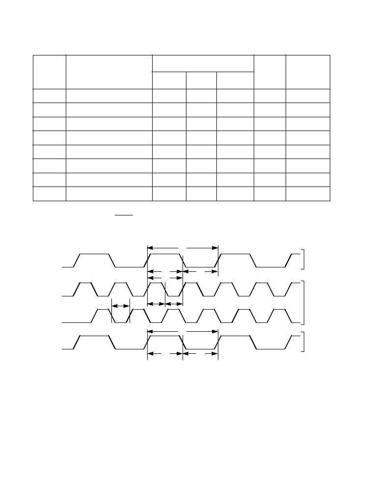
6-4
Specifications
Copyright � 2000�2001 by LSI Logic Corporation. All rights reserved.
Note:
Refer to
Figure 6.1
for timing diagram.
Figure 6.1
Input Clock Timing
Table 6.2
Input Clock Timing Characteristics
Symbol
Parameter
Limit
Unit
Conditions
Min
Typ
Max
t1
SCLK cycle time
1/33
1/66
1 MHz
t2
SCLK duty cycle
40
60
%
t3
TCLK period
7.9992
8
8.0008
ns
t4
TCLK HIGH time
3.6
4.4
ns
t5
TCLK LOW time
3.6
4.4
ns
t6
TCLK to TBC delay
0
8
ns
t7
REGCLK cycle time
1/5
1/40
1 MHz
t8
REGCLK duty cycle
40
60
%
SCLK
TCLK
TBC
REGCLK
System
Interface
t
1
t
2
t
2
t
3
t
4
t
5
t
6
t
7
t
8
t
8
10-Bit PHY
Interface
Register
Interface

AC Electrical Characteristics
6-5
Copyright � 2000�2001 by LSI Logic Corporation. All rights reserved.
Note:
Refer to
Figure 6.2
for timing diagram.
Table 6.3
Transmit System Interface Timing Characteristics
Symbol
Parameter
Limit
Unit
Conditions
Min
Typ
Max
t11
TXENn setup time
5
ns
t12
TXENn hold time
0
ns
t13
TXENn deassert time
1 SCLK
cycle
ns
t14
TXD, TXBE, TXSOFn,
TXEOF, and TXCRC
setup time
5
ns
t15
TXD, TXBE, TXSOFn,
TXEOF, and TXCRC
hold time
0
ns
t16
TXWMn delay time
0
8
ns
t17
TXWMn rise/fall time
4
ns
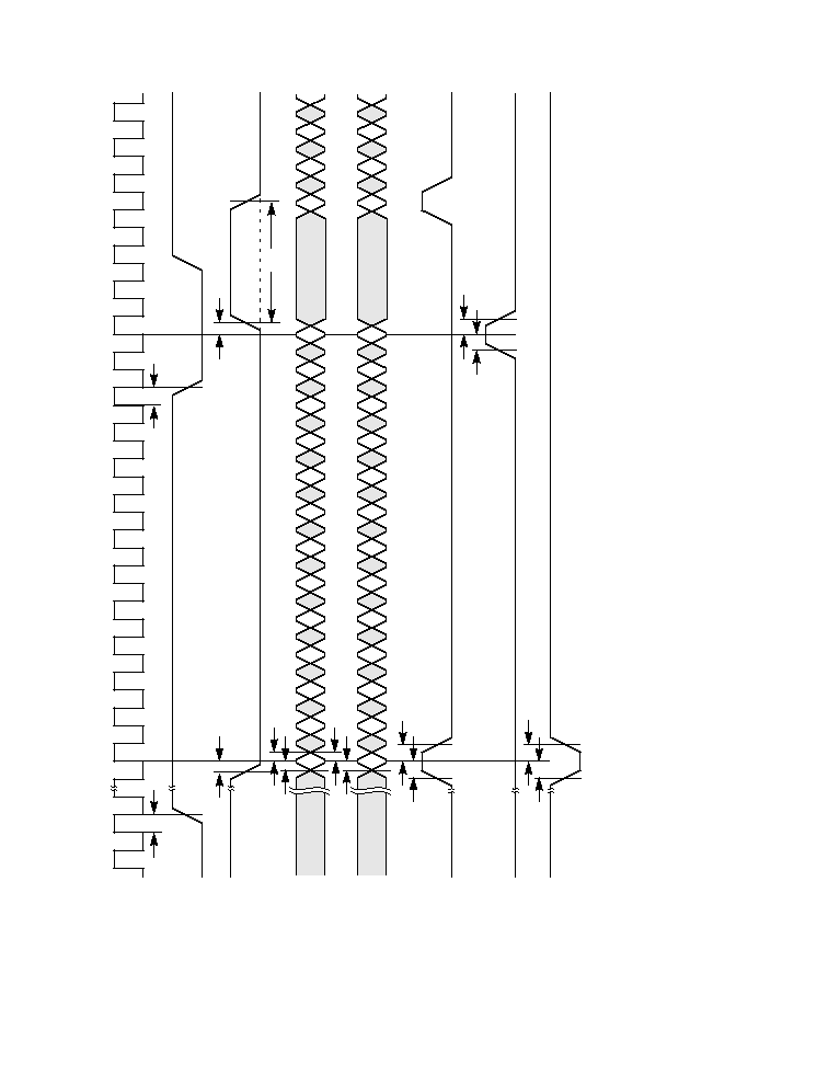
6-6
Specifications
Cop
yr
ight
�
2000�2001
b
y
LSI
Logic
Cor
por
ation.
All
r
ights
reser
v
ed.
Figure 6.2
Transmit System Interface Timing
SCLK
TXWMn[2:1]
TX_ENn
TXD[31:0]
TXBE[3:0]
TXSOF
TXEOF
TXCRCn
t
16
t
16
t
11
t
14
t
15
t
12
t
13
[1]
t
14
t
15
t
14
t
15
t
14
t
15
Note:
[1] Back-to-back packet transmission allowed without TXENn deassertion.
t
14
t
15

AC Electrical Characteristics
6-7
Copyright � 2000�2001 by LSI Logic Corporation. All rights reserved.
Note:
Refer to
Figure 6.3
�
Figure 6.5
for timing diagrams.
Table 6.4
Receive System Interface Timing Characteristics
Symbol
Parameter
Limit
Unit
Conditions
Min
Typ
Max
t31
RXENn setup time
5
ns
t32
RXENn hold time
1
ns
t33
RXENn deassert time
3 SCLK
cycles
ns
t34
RXD, RXBE, RXSOF,
RXEOF, and RXWM
delay time
0
8
ns
t35
RXD, RXBE, RXSOF,
RXEOF, and RXWM
rise/fall time
4
ns
t41
RXABORT setup time
5
ns
t42
RXABORT hold time
0
ns
t43
RXABORT assert to
RXWM deassert delay
0
1 SCLK
cycles
+ 8 ns
ns
t46
RXOEn deassert to data
High-Z delay
0
15
ns
t47
RXOEn assert to data
active delay
0
15
ns
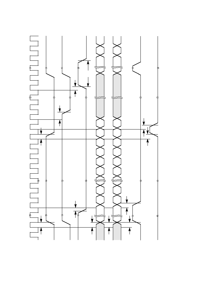
6-8
Specifications
Cop
yr
ight
�
2000�2001
b
y
LSI
Logic
Cor
por
ation.
All
r
ights
reser
v
ed.
Figure 6.3
Receive System Interface Timing
SCLK
RXWM1
RX_ENn
RXD[31:0]
RXBE[3:0]
RXSOF
RXEOF
t
34
t
34
t
31
t
33
t
34
t
34
RXWM2
t
34
t
32
t
34
First
Word
Last
Word
Status
Word
First
Word
1111
0001-
1111
t
34
1111
1111
1111
1111
1111
1111
1111
1111
1111
1111
t
34
t
34
AC Electrical Characteristics
6-9
Copyright � 2000�2001 by LSI Logic Corporation. All rights reserved.
Figure 6.4
Receive System Interface RXABORT Timing
Figure 6.5
Receive System Interface RXOEn Timing
SCLK
RXWM[2:1]
RXABORT
RXD[31:0]
RXBE[3:0]
RXSOF
RXEOF
t
41
First
Word
RX_ENn
t
43
t
42
Aborted Packet Status Word
1111
1111
11 11
1111
1111
1111
RXOEn
RXD[31:0]
RXBE[3:0]
RXSOF
RXEOF
t
46
High-Z
t
47

6-10
Specifications
Copyright � 2000�2001 by LSI Logic Corporation. All rights reserved.
Note:
Refer to
Figure 6.6
for timing diagram.
Figure 6.6
System Interface RXDC/TXDC Timing
Table 6.5
System Interface RXDC/TXDC Timing Characteristics
Symbol Parameter
Limit
Unit
Conditions
Min
Typ
Max
t51
TXDC/RXDC
assert delay time
0
8
ns
t52
TXDC/RXDC
deassert delay time
0
2 SCLK
cycle
+ 8 ns
ns
AutoClear mode off
0
3 SCLK
cycle
+ 8 ns
ns
AutoClear mode on
t53
CLR_TXDC/RXDC
setup time
5
ns
t54
CLR_TXDC/RXDC
hold time
0
ns
TXDC/RXDC
rise and fall time
4
ns
SCLK
TXENn
CLR_TXDC
TXEOF
RXEOF
t
53
TXDC
t
51
t
52
t
54
RXENn
RXDC
CLR_RXDC
Autoclear
Mode
Off
Autoclear
Mode
Off
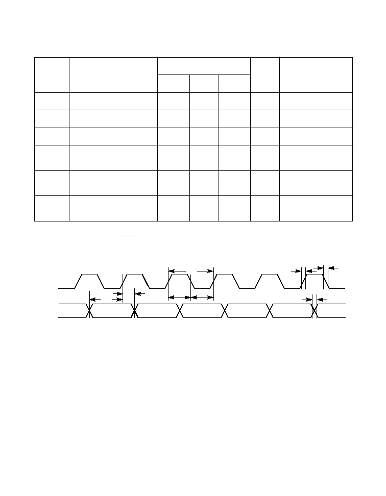
AC Electrical Characteristics
6-11
Copyright � 2000�2001 by LSI Logic Corporation. All rights reserved.
Note:
Refer to
Figure 6.7
for timing diagram.
Figure 6.7
Transmit 10-Bit PHY Interface Timing
Table 6.6
Transmit 10-Bit PHY Interface Timing Characteristics
Symbol
Parameter
Limit
Unit
Conditions
Min
Typ
Max
t61
TBC period
7.992
8
8.008
ns
t62
TBC HIGH time
3.2
4.8
ns
t63
TBC LOW time
3.2
4.8
ns
t64
TX[0:9] data valid before
TBC rising edge
2.0
ns
Assumes TBC duty
cycle = 40
-
60%
t65
TX[0:9] data valid after
TBC rising edge
1.0
ns
Assumes TBC duty
cycle = 40�60%
t66
TBC, TX[0:9]
rise and fall time
0.7
2.4
ns
t
66
TBC
TX[0:9]
t
62
t
63
t
61
t
64
t
65
t
66
t
66
6-12
Specifications
Copyright � 2000�2001 by LSI Logic Corporation. All rights reserved.
Note:
Refer to
Figure 6.8
for timing diagram.
Figure 6.8
Receive 10-Bit PHY Interface Timing
Table 6.7
Receive 10-Bit PHY Interface Timing Characteristics
Symbol
Parameter
Limit
Unit
Conditions
Min
Typ
Max
t
71
RBC frequency
62.4937
62.5
62.5063
MHz
t
72
RBC HIGH time
6.4
9.6
ns
6.4
128
ns
During
synchronization
t
73
RBC LOW time
6.4
9.6
ns
6.4
128
ns
During
synchronization
t
74
RBC skew
7.5
8.5
ns
t
75
RX[0:9] setup time
2.5
ns
t
76
RX[0:9] hold time
1.5
ns
t
77
RBC, RX[0:9]
rise and fall time
0.7
2.4
ns
t
76
t
75
t
77
RBC1
RX[0:9]
t
74
t
77
t
77
t
77
t
71
t
76
t
75
t
72
t
73
t
72
t
73
t
71
t
77
RBC0

AC Electrical Characteristics
6-13
Copyright � 2000�2001 by LSI Logic Corporation. All rights reserved.
Note:
Refer to
Figure 6.9
and
Figure 6.10
for timing diagrams.
Table 6.8
Register Interface Timing Characteristics
Symbol
Parameter
Limit
Unit
Conditions
Min
Typ
Max
t81
REGCSn, REGWRn,
REGRDn, REGA, REGD
setup time
10
ns
t82
REGCSn, REGWRn,
REGRDn, REGA, REGD
hold time
1
ns
t83
REGCLK to REGD
active delay
10
ns
Read cycle.
All registers except
Counter Registers 1�53
6
REGCLK
cycles +
10 ns
ns
Read cycle. Counter
Registers 1�53, first 16
bits of counter result
3
REGCLK
cycles +
10 ns
ns
Read cycle. Counter
Registers 1�53, second
16 bits of counter result
t84
REGCLK to REGD
3-state delay
0
10
ns
t85
REGCLK to REGINT
assert delay
0
20
ns
t86
REGCLK to REGINT
deassert delay
0
20
ns
t87
Deassertion time between
reads
4
REG-
CLK

6-14
Specifications
Copyright � 2000�2001 by LSI Logic Corporation. All rights reserved.
Figure 6.9
Register Interface Timing (Excluding Counter Read Cycle)
REGCLK
REGWRn
t
7
t
8
t
8
REGCSn
REGRDn
REGD[15:0]
REGA{7:0]
REGINT
t
81
t
82
t
81
t
82
t
81
t
82
t
81
t
82
Data In
t
81
t
82
High-Z
t
83
Data Out
t
85
t
86
t
84
Write Cycle
REGD[15:0] Is Input
Read Cycle
REGD[15:0] is Output
High-Z
High-Z

AC Electrical Characteristics
6-15
Copyright � 2000�2001 by LSI Logic Corporation. All rights reserved.
Figure 6.10 Register Interface Timing, Counter Read Cycle (of the Same Counter)
Not Valid
REGCLK
REGWRn
REGCSn
REGRDn
REGD[15:0]
REGAD[15:0]
t
81
t
82
t
84
t
84
3
1
2
1
6
t
81
t
82
t
84
2nd Counter Address
1st Counter Address
t
81
t
84
High-Z
t
83
2nd 16 Bits of
Counter Result
Not Valid
1st 16 Bits of
Counter Result
t
83
High-Z

6-16
Specifications
Copyright � 2000�2001 by LSI Logic Corporation. All rights reserved.
Figure 6.11 Register Interface Timing, Counter Read Cycle (Between Different
Counters)
Not Valid
REGCLK
REGWRn
REGCSn
REGRDn
REGD[15:0]
REGAD[15:0]
t
81
t
82
t
84
t
84
t
81
Counter Address A
t
81
t
84
High-Z
t
83
16 Bits of
Counter Results
Not Valid
t
83
High-Z
t
81
t
81
t
82
t
81
Counter Address B
t
87
16 Bits of
Counter Results
t
84
Hi-Z
t
82
t
82
t
82
t
82
Note: No burst reading,

8101/8104 Pinouts and Pin Listings
6-17
Copyright � 2000�2001 by LSI Logic Corporation. All rights reserved.
6.4 8101/8104 Pinouts and Pin Listings
Figure 6.12
shows the pinout and
Table 6.9
lists the pins for the 8101
and
Figure 6.13
shows the pinout and
Table 6.10
lists the pins for the
8104.
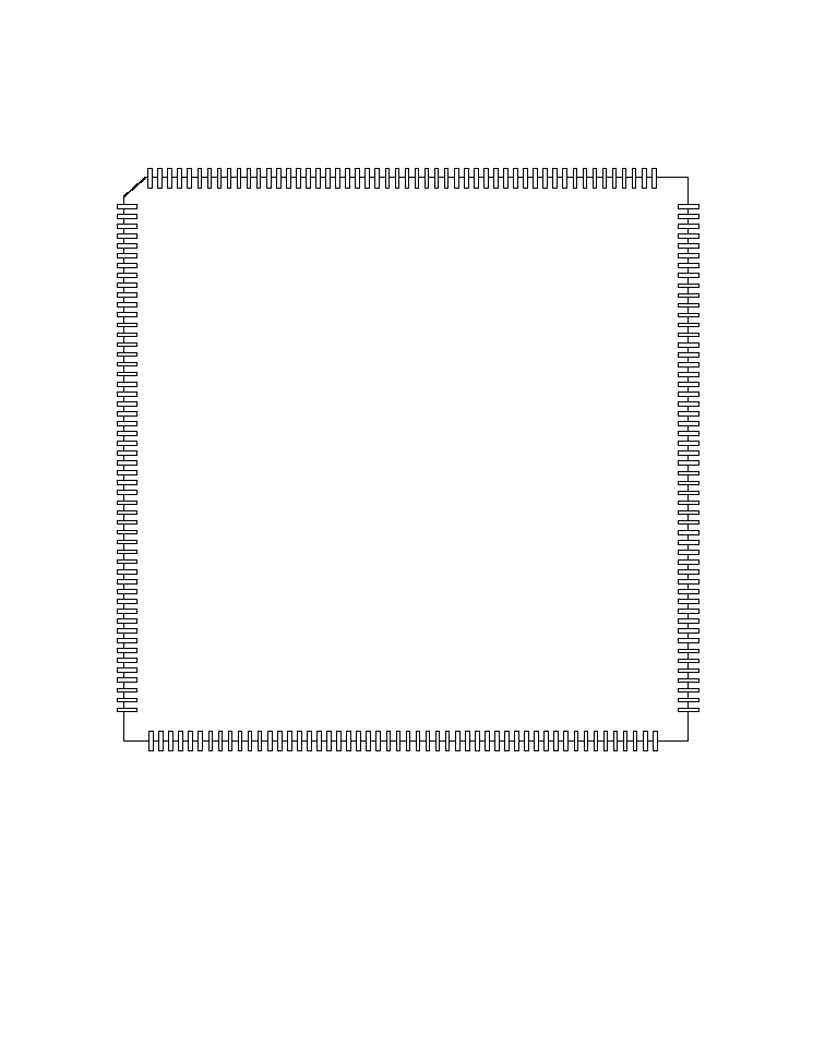
6-18
Specifications
Copyright � 2000�2001 by LSI Logic Corporation. All rights reserved.
Figure 6.12 8101 208-Pin PQFP Pinout
1
3
5
7
9
11
13
15
17
19
21
23
25
27
29
31
33
35
36
37
38
39
40
42
44
46
48
50
52
8101
2
4
6
8
10
12
14
16
18
20
22
24
26
28
30
32
34
41
43
45
47
49
51
156
154
152
150
148
146
144
142
140
138
136
134
132
130
128
126
124
122
121
120
119
118
117
115
113
111
109
107
105
155
153
151
149
147
145
143
141
139
137
135
133
131
129
127
125
123
116
114
112
110
108
106
157
159
161
163
165
167
169
171
173
175
177
179
181
183
185
187
189
191
192
193
194
195
196
198
200
202
204
206
208
158
160
162
164
166
168
170
172
174
176
178
180
182
184
186
188
190
197
199
201
203
205
207
53
55
57
59
61
63
65
67
69
71
73
75
77
79
81
83
85
87
88
89
90
91
92
94
96
98
100
102
104
54
56
58
60
62
64
66
68
70
72
74
76
78
80
82
84
86
93
95
97
99
101
103
RXENn
RXOEn
GND
VCC
VCC
VCC
RESERVED
VCC
VCC
TAP
VCC
TEST
SD
GND
RX0
RX1
RX2
RX3
RX4
GND
RX5
RX6
RX7
RX8
RX9
RBC0
GND
RBC1
LCK_REFn
VCC
EN_CDET
TBC
GND
EWRAP
TX9
GND
TX8
TX7
GND
TX6
TX5
GND
TX4
VCC
TX3
GND
TX2
TX1
GND
TX0
GND
TCLK
RXWM1
RXWM2
RXDC
CLR_RXDC
RXABORT
VCC
GND
SCLK
VCC
VCC
TXENn
TXSOF
TXEOF
GND
TXBE0
TXBE1
TXBE2
TXBE3
GND
TXWM1n
TXWM2n
VCC
TXDC
CLR_TXDC
TXCRCn
TXD0
TXD1
TXD2
TXD3
TXD4
TXD5
TXD6
TXD7
GND
TXD8
TXD9
TXD10
TXD11
TXD12
TXD13
TXD14
VCC
TXD15
TXD16
GND
TXD17
TXD18
TXD19
TXD20
TXD21
TXD22
TXD23
VCC
RXEOF
RXSOF
RXBE3
RXBE2
RXBE1
RXBE0
GND
RXD0
RXD1
RXD2
RXD3
GND
RXD4
RXD5
VCC
VCC
RXD6
RXD7
GND
RXD8
RXD9
RXD10
RXD11
GND
RXD12
RXD13
VCC
RXD14
RXD15
GND
RXD16
RXD17
RXD18
RXD19
GND
RXD20
RXD21
VCC
RXD22
RXD23
GND
RXD24
RXD25
RXD26
RXD27
GND
RXD28
RXD29
VCC
RXD30
RXD31
VCC
LINKn
REGA0
REGA1
REGA2
REGA3
GND
REGA4
REGA5
REGA6
REGA7
REGINT
REGWRn
REGRDn
GND
REGCLK
REGD15
VCC
REGD14
REGD13
REGD12
GND
REGD11
REGD10
REGD9
REGD8
GND
REGD7
VCC
REGD6
REGD5
REGD4
GND
REGD3
REGD2
REGD1
REGD0
GND
GND
REGCSn
RESER
VED
RESETn
FCNTRL
TXD31
VCC
TXD30
TXD29
TXD28
TXD27
TXD26
TXD25
TXD24
208 PQFP
Top View

8101/8104 Pinouts and Pin Listings
6-19
Copyright � 2000�2001 by LSI Logic Corporation. All rights reserved.
Table 6.9
8101 208-Pin PQFP Pin List (Alphabetical Listing)
TXD21
107
TXD22
106
TXD23
105
TXD24
104
TXD25
103
TXD26
102
TXD27
101
TXD28
100
TXD29
99
TXD30
98
TXD31
96
TXDC
134
TXENn
146
TXEOF
144
TXSOF
145
TXWM1n
137
TXWM2n
136
VCC
4
VCC
5
VCC
6
VCC
8
VCC
9
VCC
11
VCC
30
VCC
44
VCC
53
VCC
70
VCC
81
VCC
97
VCC
115
VCC
135
VCC
147
VCC
148
VCC
151
VCC
159
VCC
170
VCC
181
VCC
193
VCC
192
VCC
208
Signal
Pin
Signal
Pin
CLR_RXDC
153
CLR_TXDC
133
EN_CDET
31
EWRAP
34
FCNTRL
95
GND
3
GND
14
GND
20
GND
27
GND
33
GND
36
GND
39
GND
42
GND
46
GND
49
GND
51
GND
59
GND
67
GND
74
GND
79
GND
85
GND
90
GND
91
GND
112
GND
123
GND
138
GND
143
GND
150
GND
162
GND
167
GND
173
GND
178
GND
184
GND
189
GND
196
GND
201
LCK_REFn
29
LINKn
54
RBC0
26
RBC1
28
REGA0
55
REGA1
56
REGA2
57
REGA3
58
REGA4
60
REGA5
61
REGA6
62
REGA7
63
REGCLK
68
REGCSn
92
REGD0
89
REGD1
88
REGD2
87
REGD3
86
REGD4
84
REGD5
83
REGD6
82
REGD7
80
REGD8
78
REGD9
77
REGD10
76
REGD11
75
REGD12
73
REGD13
72
REGD14
71
REGD15
69
REGINT
64
REGRDn
66
REGWRn
65
RESERVED
7
RESERVED
93
RESETn
94
RX0
15
RX1
16
RX2
17
RX3
18
RX4
19
RX5
21
RX6
22
RX7
23
RX8
24
RX9
25
RXABORT
152
RXBE0
202
RXBE1
203
RXBE2
204
RXBE3
205
RXD0
200
RXD1
199
RXD2
198
RXD3
197
RXD4
195
RXD5
194
RXD6
191
RXD7
190
RXD8
188
RXD9
187
RXD10
186
RXD11
185
RXD12
183
RXD13
182
RXD14
180
RXD15
179
RXD16
177
RXD17
176
RXD18
175
RXD19
174
RXD20
172
RXD21
171
RXD22
169
RXD23
168
RXD24
166
RXD25
165
RXD26
164
RXD27
163
RXD28
161
RXD29
160
RXD30
158
RXD31
157
RXDC
154
RXENn
1
RXEOF
207
RXOEn
2
RXSOF
206
RXWM1
156
RXWM2
155
SCLK
149
SD
13
TAP
10
TBC
32
TCLK
52
TEST
12
TX0
50
TX1
48
TX2
47
TX3
45
TX4
43
TX5
41
TX6
40
TX7
38
TX8
37
TX9
35
TXBE0
142
TXBE1
141
TXBE2
140
TXBE3
139
TXCRCn
132
TXD0
131
TXD1
130
TXD2
129
TXD3
128
TXD4
127
TXD5
126
TXD6
125
TXD7
124
TXD8
122
TXD9
121
TXD10
120
TXD11
119
TXD12
118
TXD13
117
TXD14
116
TXD15
114
TXD16
113
TXD17
111
TXD18
110
TXD19
109
TXD20
108
Signal
Pin
Signal
Pin
Signal
Pin

6-20
Specifications
Copyright � 2000�2001 by LSI Logic Corporation. All rights reserved.
Figure
6.13
8104
208-Pin
BGA
Pinout
A1
A2
A3
A4
A5
A6
A7
A8
A9
A10
A11
A12
A13
A14
A15
A16
VCC
RXEOF
RXBE3
RXD0
RXD4
VCC
RXD7
RXD11
RXD16
RXD20
RXD21
RXD23
RXD27
RXD29
RXD30
RXD31
B1
B2
B3
B4
B5
B6
B7
B8
B9
B10
B11
B12
B13
B14
B15
B16
RXOEn
RXENn
RXSOF
RXBE2
RXD2
VCC
RXD8
RXD10
RXD15
RXD19
VCC
RXD25
RXD28
VCC
RXWM1
RXWM2
C1
C2
C3
C4
C5
C6
C7
C8
C9
C10
C
11
C12
C
13
C14
C
15
C16
GND
VCC
VCC
RXBE1
RXD3
VCC
RXD6
RXD12
RXD14
RXD18
RXD22
RXD26
GND
RXABOR
T
CLR_RXDC
TXDC
D1
D2
D3
D4
D5
D6
D7
D8
D9
D10
D
11
D12
D
13
D14
D
15
D16
VCC
VCC
RESER
VED
RXBE0
RXD1
RXD5
RXD9
RXD13
VCC
RXD17
VCC
RXD24
VCC
VCC
SLCK
VCC
E1
E2
E3
E4
E13
E14
E15
E16
VCC
T
A
P
VCC
TEST
GND
TXEOF
TXSOF
TXENn
F1
F2
F3
F4
F13
F14
F15
F16
SD
RX0
RX1
RX2
TXBE3
TXBE2
TXBE0
TXBE1
G1
G2
G3
G4
G7
G8
G9
G10
G
13
G14
G
15
G16
RX4
RX3
RX5
RX6
GND
GND
GND
GND
TXDC
VCC
TXWM2n
TXWM1n
H1
H2
H3
H4
H7
H8
H9
H10
H
13
H14
H
15
H16
RX8
RX7
RX9
RBC0
GND
GND
GND
GND
TXD1
TXD0
TXCRCn
CLR_TXDC
J1
J2
J3
J4
J7
J8
J9
J10
J13
J14
J15
J16
RBC1
LCK_REFn
VCC
VCC
GND
GND
GND
GND
TXD2
TXD3
TXD5
TXD4
K1
K2
K3
K4
K7
K8
K9
K10
K13
K14
K15
K16
TBC
EN_CDET
EWRAP
TX9
GND
GND
GND
GND
TXD6
TXD7
GND
TXD8
L1
L2
L3
L4
L13
L14
L15
L16
TX7
TX8
GND
TX6
TXD9
TXD10
TXD11
TXD12
M1
M2
M3
M4
M13
M
14
M15
M
16
GND
TX5
TX4
VCC
TXD13
TXD14
TXD15
VCC
N1
N2
N3
N4
N5
N6
N7
N8
N9
N10
N
11
N12
N
13
N14
N
15
N16
TX3
TX2
GND
GND
REGWRn
REGD15
REGD12
REGD8
REGD7
REGD5
REGD1
RESER
VED
VCC
TXD17
TXD18
TXD16
P1
P2
P3
P4
P5
P6
P7
P8
P9
P10
P11
P12
P13
P14
P15
P16
TX1
TCLK
REGA3
REGA5
REGINT
REGCLK
REGD13
REGD9
REGD6
REGD4
REGD0
RESETn
TXD30
TXD19
TXD22
TXD20
R1
R2
R3
R4
R5
R6
R7
R8
R9
R10
R
11
R12
R
13
R14
R
15
R16
TX0
VCC
REGA2
REGA4
REGA6
REGRDn
VCC
REGD11
VCC
REGD2
GND
TXD31
TXD28
TXD27
TXD23
TXD21
T1
T2
T3
T4
T5
T6
T7
T8
T9
T10
T11
T12
T13
T14
T15
T16
LINKn
REGA0
REGA1
GND
REGA7
GND
REGD14
REGD10
VCC
REGD3
REGCSn
FCNTRL
TXD29
TXD26
TXD25
TXD24

8101/8104 Pinouts and Pin Listings
6-21
Copyright � 2000�2001 by LSI Logic Corporation. All rights reserved.
Table 6.10
8104 208-Pin BGA Pin List (Alphabetical Listing)
TXD25
T15
TXD26
T14
TXD27
R14
TXD28
R13
TXD29
T13
TXD30
P13
TXD31
R12
TXDC
G13
TXENn
E16
TXEOF
E14
TXSOF
E15
TXWM1n
G16
TXWM2n
G15
VCC
A01
VCC
A06
VCC
B06
VCC
B11
VCC
B14
VCC
C02
VCC
C03
VCC
C06
VCC
D01
VCC
D02
VCC
D09
VCC
D11
VCC
D13
VCC
D14
VCC
D16
VCC
E01
VCC
E03
VCC
G14
VCC
J03
VCC
J04
VCC
M04
VCC
M16
VCC
N13
VCC
R02
VCC
R07
VCC
R09
VCC
T09
Signal
Pin
Signal
Pin
CLR_RXDC C15
CLR_TXDC
H16
EN_CDET
K02
EWRAP
K03
FCNTRL
T12
GND
C01
GND
C13
GND
E13
GND
G07
GND
G08
GND
G09
GND
G10
GND
H07
GND
H08
GND
H09
GND
H10
GND
J07
GND
J08
GND
J09
GND
J10
GND
K07
GND
K08
GND
K09
GND
K10
GND
K15
GND
L03
GND
M01
GND
N03
GND
N04
GND
R11
GND
T04
GND
T06
LCK_REFn
J02
LINKn
T01
RBC0
H04
RBC1
J01
REGA0
T02
REGA1
T03
REGA2
R03
REGA3
P03
REGA4
R04
REGA5
P04
REGA6
R05
REGA7
T05
REGCLK
P06
REGCSn
T11
REGD0
P11
REGD1
N11
REGD2
R10
REGD3
T10
REGD4
P10
REGD5
N10
REGD6
P09
REGD7
N09
REGD8
N08
REGD9
P08
REGD10
T08
REGD11
R08
REGD12
N07
REGD13
P07
REGD14
T07
REGD15
N06
REGINT
P05
REGRDn
R06
REGWRn
N05
RESERVED D03
RESERVED N12
RESETn
P12
RX0
F02
RX1
F03
RX2
F04
RX3
G02
RX4
G01
RX5
G03
RX6
G04
RX7
H02
RX8
H01
RX9
H03
RXABORT
C14
RXBE0
D04
RXBE1
C04
RXBE2
B04
RXBE3
A03
RXD0
A04
RXD1
D05
RXD2
B05
RXD3
C05
RXD4
A05
RXD5
D06
RXD6
C07
RXD7
A07
RXD8
B07
RXD9
D07
RXD10
B08
RXD11
A08
RXD12
C08
RXD13
D08
RXD14
C09
RXD15
B09
RXD16
A09
RXD17
D10
RXD18
C10
RXD19
B10
RXD20
A10
RXD21
A11
RXD22
C11
RXD23
A12
RXD24
D12
RXD25
B12
RXD26
C12
RXD27
A13
RXD28
B13
RXD29
A14
RXD30
A15
RXD31
A16
RXDC
C16
RXENn
B02
RXEOF
A02
RXOEn
B01
RXSOF
B03
RXWM1
B15
RXWM2
B16
SCLK
D15
SD
F01
TAP
E02
TBC
K01
TCLK
P02
TEST
E04
TX0
R01
TX1
P01
TX2
N02
TX3
N01
TX4
M03
TX5
M02
TX6
L04
TX7
L01
TX8
L02
TX9
K04
TXBE0
F15
TXBE1
F16
TXBE2
F14
TXBE3
F13
TXCRCn
H15
TXD0
H14
TXD1
H13
TXD2
J13
TXD3
J14
TXD4
J16
TXD5
J15
TXD6
K13
TXD7
K14
TXD8
K16
TXD9
L13
TXD10
L14
TXD11
L15
TXD12
L16
TXD13
M13
TXD14
M14
TXD15
M15
TXD16
N16
TXD17
N14
TXD18
N15
TXD19
P14
TXD20
P16
TXD21
R16
TXD22
P15
TXD23
R15
TXD24
T16
Signal
Pin
Signal
Pin
Signal
Pin

6-22
Specifications
Copyright � 2000�2001 by LSI Logic Corporation. All rights reserved.
6.5 Package Mechanical Dimensions
The 8101 Gigabit Ethernet Controller is available in the 208-pin Plastic
Quad Flat Pack (PQFP) as shown in
Figure 6.14
. and the 8104 Ball Grid
Array Package as shown in
Figure 6.15
.
Figure 6.14 208-Pin PQFP Mechanical Drawing
Note:
This drawing may not be the latest version.
30. 60
�
0. 30
28. 00
0. 20
1. 25
0. 20
0.10
0. 50
0. 25 min.
0.15
0.10 � 0. 05
0.10 MAX
#1
See Detail A
0
-
8 �
0. 50
0. 20
Detail A
3.40
�
0. 20
4.10 Max.
#208
�
�
30.
60
�
0.
30
28.
00
0.
20
�
�
1. All Dimensions are in (millimeters)
�

Package Mechanical Dimensions
6-23
Copyright � 2000�2001 by LSI Logic Corporation. All rights reserved.
Figure 6.15 208 mini-BGA (HG) Mechanical Drawing
Important:
This drawing may not be the latest version. For board layout and manufacturing, obtain the
most recent engineering drawings from your LSI Logic marketing representative by
requesting the outline drawing for package code HG.

6-24
Specifications
Copyright � 2000�2001 by LSI Logic Corporation. All rights reserved.

Customer Feedback
We would appreciate your feedback on this document. Please copy the
following page, add your comments, and fax it to us at the number
shown.
If appropriate, please also fax copies of any marked-up pages from this
document.
Important:
Please include your name, phone number, fax number, and
company address so that we may contact you directly for
clarification or additional information.
Thank you for your help in improving the quality of our documents.

Customer Feedback
Reader's Comments
Fax your comments to:
LSI Logic Corporation
Technical Publications
M/S E-198
Fax: 408.433.4333
Please tell us how you rate this document: 8101/8104 Gigabit Ethernet
Controller. Place a check mark in the appropriate blank for each
category.
What could we do to improve this document?
If you found errors in this document, please specify the error and page
number. If appropriate, please fax a marked-up copy of the page(s).
Please complete the information below so that we may contact you
directly for clarification or additional information.
Excellent Good Average
Fair
Poor
Completeness of information
____
____
____
____
____
Clarity of information
____
____
____
____
____
Ease of finding information
____
____
____
____
____
Technical content
____
____
____
____
____
Usefulness of examples and
illustrations
____
____
____
____
____
Overall manual
____
____
____
____
____
Name
Date
Telephone
Title
Company Name
Street
City, State, Zip
Department
Mail Stop
Fax

You can find a current list of our U.S. distributors, international distributors, and sales
offices and design resource centers on our web site at
http://www.lsilogic.com/contacts/na_salesoffices.html
