
3, 4 AND 8 PIN AUTOMATIC SHUT-OFF TIMERS
January 2002
DESCRIPTION
The basic ASOT is a CMOS integrated circuit timer that can
be mask programmed from 2.5 minutes to 32 hours as shown in
Table 1. The output of the IC is used to turn on a 12V relay and
has a duty cycle which can be mask programmed from 5% to
37.5% in 2.5% steps as shown in Table 2. The duty cycle can
be selected to optimize operation for a particular relay coil.
There are 5 different versions of the IC.
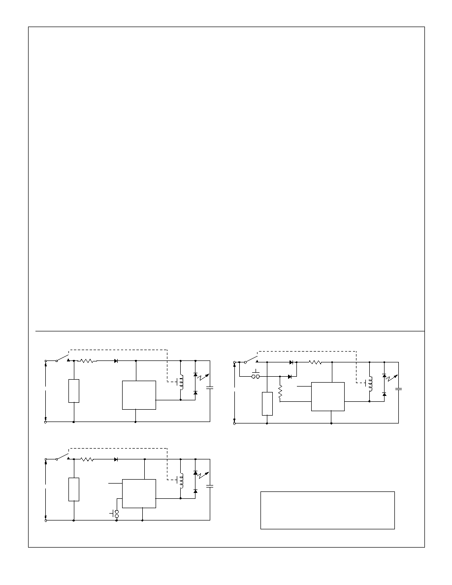
The ASOT is a 3-Pin version housed in a TO-92 package. The
application schematic is shown in Figure 2. When latching
switch S1 is closed, the output turns on energizing relay L1 and
keeping switch S1 closed. When the programmed time-out
expires, the output turns off deenergizing relay L1 and causing
switch S1 to open.
The ASOTR is a 4-Pin version as shown in Figure 3. The out-
put turns on in the same manner as in the 3-Pin version. If
momentary switch S2 is closed, the timer resets and starts
timing out again. The S2 input has an internal pull-up resistor.
Every subsequent momentary switch closure resets the timer.
As in the 3-Pin version, the output remains on until the timeout
expires.
The ASOTT is also a 4-Pin version as shown in Figure 4. In
this version contacts C1 replace switch S1 and are not
accessible. The application of power caused by closing
LSI/CSI
LSI Computer Systems, Inc. 1235 Walt Whitman Road, Melville, NY 11747 (631) 271-0400 FAX (631) 271-0405
ASOT
ASOTR ASOTR1
ASOTT
ASOTT1
UL
Æ
A3800
1
2
3
4
8
5
6
7
V
DD
GND
OUT
IN
NC
NC
NC
DUTY CYCLE IN
V
DD
GND OUT
IN
V
DD
GND
OUT
FIGURE 1. PACKAGE OPTIONS
DIP/SOIC
T O - 9 2
SIP
8-PIN VERSION
4-PIN VERSION
3-PIN VERSION
1
2
3
4
ASOTR1
and
ASOTT1
ASOT
ASOTR
and
ASOTT
the momentary switch S2 causes the output to toggle on as in
the 3-Pin version. If the momentary switch is closed again,
the output toggles off causing contact C1 to open and power
to be removed. The R2 input has an internal pull-up resistor.
The default operaton of the output produces a double duty
cycle for the first 10 milliseconds of output activation to
increase the pull-in torque of the relay. The option to remove
this feature is factory selectable in the ASOT (3-Pin), ASOTR
(4-Pin) and ASOTT (4-Pin) versions. There are also two 8-Pin
versions available which allow the user to change this feature.
The ASOTR1 is the 8-Pin version used in the Figure 3
application and the ASOTT1 is the 8-Pin version used in the
Figure 4 application. In both cases, the duty cycle input has
an internal pull-up resistor. Tying the input to Vss removes
the double duty cycle feature.
ADVANCE INFORMATION
FEATURES:
∑ Minimizes external components and power consumption
∑ Factory calibrated timer
∑ Mask programmable from 2.5 minutes to 32 hours
APPLICATIONS
Control of household appliances, heaters, lighting and AC motors.
Timeout
Numbers Auto Shut-Off Times
01 - 10
0h
0h
0h
0h
0h
0h
0h
0h
0h
0h
2.5m
5m
7.5m
10m
12.5m
15m
17.5m
20m
22.5m
25m
11 - 20
0h
0h
0h
0h
0h
0h
0h
1h
1h
1h
30m
35m
37.5m
40m
45m
50m
52.5m
0m
10m
15m
21 - 30
1h
1h
1h
1h
2h
2h
2h
2h
3h
3h
20m
30m
40m
45m
0m
20m
30m
40m
0m
20m
31 - 40
3h
4h
4h
5h
5h
6h
6h
7h
8h
9h
30m
0m
40m
0m
20m
0m
40m
0m
0m
0m
41 - 50
9h
10h
10h
12h
14h
16h
20h
24h
28h
32h
20m
0m
40m
0m
0m
0m
0m
0m
0m
0m
Duty Cycle Numbers Duty Cycle Percentages
01 - 07
5
7.5
10
12.5
15
17.5
20
08 - 14
22.5
25
27.5
30
32.5
35
37.5
TABLE 1
TABLE 2
7214-011702-1
ABSOLUTE MAXIMUM RATINGS:
(All voltages referenced to V
SS
)
SYMBOL
VALUE
UNIT
Maximum
V
DD
+85
V
Input
V
IN
+5 to V
ss
- 0.3
V
Operating Temperature
T
A
0 to +85
∞C
Storage Temperature
T
STG
-65 to +150
∞C
7214-011702-2
ELECTRICAL CHARACERISTICS:
(All voltages referenced to Vss)
PARAMETER
SYMBOL
MIN
TYP
MAX
UNIT
CONDITION
Shunt Regulator Voltage
V
DD
70
75
80
V
-
Regulator Sink Current
I
SK
-
-
10
mA
-
Supply Current
I
DD
-
-
370
µA
V
DD
= 48V
Power-On-Reset
V
POR
32
37
42
V
-
POR Hysteresis
V
HYS
7
-
12
V
-
Output Driver - ON
I
O
70
-
-
mA
Vo = 5V
I
O
50
-
-
mA
Vo = 3V
Output Driver - OFF
I
O
-
-
50
µA
Vo = V
DD
Output Frequency
F
O
20.5
21.8
23.11
kHz
-
Switch On Delay
S
OD
-
47
-
ms
V
DD
> V
POR
INPUT
Switching Voltage
V
SW
-
-
2.5
V
ASOTR, ASOTT
Source Current
I
SC
-
20
-
µA
ASOTR
@V
IN
= 0V
Positive Clamp Voltage
V
PC
-
-
4
V
ASOTT
@Input Sink Current = 350µA
Negative Clamp Voltage
V
NC
-
-
1
V
ASOTT
@Input Sink Current = 350µA
Duty Cycle Select
I
DC
-
20
-
µA
ASOTR1, ASOTT1
Source Current
@V
IN
= 0V
V
DD
L
O
A
D
Vss
OUT
C1
D2
D1
R1
FIGURE 2. ASOT
V
DD
L
O
A
D
Vss
OUT
C1
D2
D1
R1
IN
L1
L1
S1
S1
S2
AC
AC
DUTY
CYCLE
*
FIGURE 3. ASOTR, ASOTR1
*
This input available only for ASOTR1
V
DD
L
O
A
D
Vss
OUT
C1
D3
D1
R1
IN
L1
S1
AC
DUTY
CYCLE
*
FIGURE 4. ASOTT, ASOTT1
*
This input available only for ASOTT1
D2
C1
R2
The information included herein is believed to be
accurate and reliable. However, LSI Computer Systems,
Inc. assumes no responsibilities for inaccuracies, nor for
any infringements of patent rights of others which may
result from its use.