 | –≠–ª–µ–∫—Ç—Ä–æ–Ω–Ω—ã–π –∫–æ–º–ø–æ–Ω–µ–Ω—Ç: LS7501 | –°–∫–∞—á–∞—Ç—å:  PDF PDF  ZIP ZIP |

TONE ACTIVATED TELEPHONE LINE SWITCH CONTROLLERS
FEATURES:
∑ Circuit activated by Tone with specific Frequency and
Time Duration.
∑ Frequency and Time Duration values are mask
programmable.
∑ Small Signal (as low as - 30 DBM) and Digital Level
Tone signals accommodated.
∑ On-chip active oscillator network and 32,768 Hz
Crystal generates timing.
∑ Low power consumption.
∑ +4.0V to +6V operation (V
DD
- V
SS
).
APPLICATIONS:
∑ Remote telephone line testing
∑ Remote meter reading
∑ Security system dialers.
GENERAL DESCRIPTION:
The LS7501 - LS7510 are CMOS frequency discriminator
circuits designed to respond to a specific frequency
TONE signal when that frequency is maintained within
+10Hz during a continuous 4.5 second Sample Interval
Time. When a valid TONE occurs the Set Relay Level
output goes high for 20 seconds.
A typical application will use the Set Relay Level output
to temporarily switch the telephone line connection.
Valid Frequencies are mask programmable from 11Hz to
4095 Hz, in 1 Hz steps. Valid Sample Interval Times are
mask-programmable from 0.5 seconds to 8.0 seconds, in
0.5 second steps. Table 1 shows mask programmable
options for the available LS7501 - LS7510 part numbers.
Table 1. MASK PROGRAMMED OPTIONS
Part # Frequency (Hz) Part # Frequency (Hz)
LS7501
2683 LS7506 2863
LS7502
2713 LS7507 2893
LS7503
2743 LS7508 2923
LS7504
2773 LS7509 2953
LS7505
2833 LS7510 2983
NOTE: All Part Numbers are programmed with a Sample
Interval Time of 4.5 seconds. Referring to the LS75XX
Block Diagram (Figure 2) each Part Number has the Set
Relay Level option on Pin 8. The 32 KHz option is on Pin
2 with one exception. LS7502 has the 8Hz option.
1
2
3
4
5
6
7
8
12
13
14
15
16
LSI
9
10
11
V
DD (+V)
X2
X1
DIGITAL TONE
AMP IN
AMP OUT
RESET
V
SS (-V)
DTO
TIME BASE
VF OUT
VI OUT
FDEN
DTEN INPUT
SET RELAY PULSE
SET RELAY LEVEL
FIGURE 1
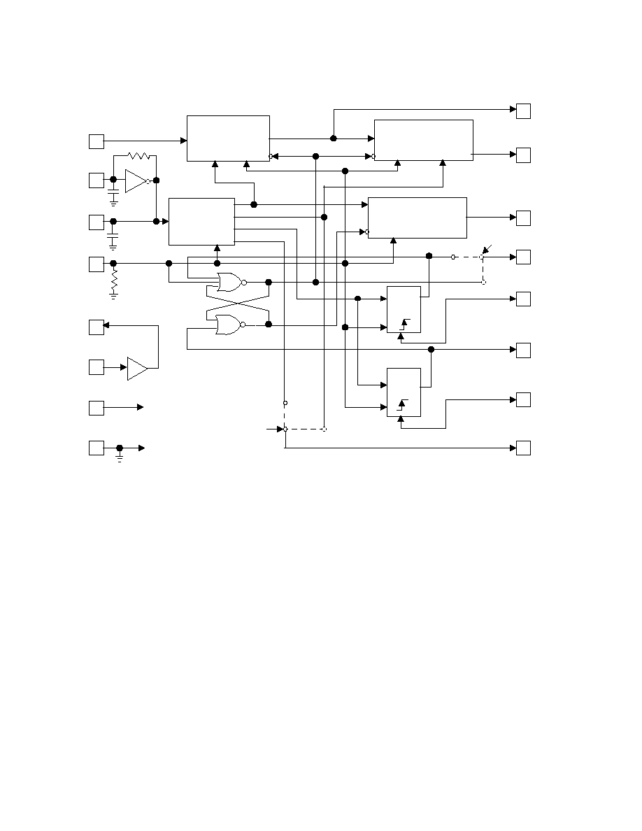
CIRCUIT OPERATION:
Referencing Figure 2, an external C is used to generate a
Power-On Reset pulse at Pin 10. When the Frequency Dis-
criminator samples a valid frequency at Pin 13 for an entire
0.5 second sample period, Pin 3 goes high and the Sample
Interval Timer begins timing. If the Pin 13 frequency is not
valid during any subsequent sample period, Pin 3 goes low
and resets the Sample Interval Timer. When Pin 13 fre-
quency is valid for the programmed period of the Sample In-
terval Timer, a high-going pulse occurs at Pin 4. Normally,
Pin 4 externally connects to Pin 6 and the pulse will cause
the Frequency Discriminator to be disabled, enable the Dis-
connect Timer and bring Set Relay Level high at Pin 8.
When the Disconnect Timer times out (20 seconds) a high-
going pulseoccurs at Pin 1. Normally, Pin 1 externally con-
nects to Pin 5 and the pulse will cause the Frequency Dis-
criminator to be enabled, disable the Disconnect Timer and
bring Set Relay Level low at Pin 8. The circuit operating se-
quence begins again.
A digital level Tone signal connects to Pin 13. A small-signal
Tone frequency should be AC coupled to Pin 12 with Pin 11
externally connected to Pin 13. The 32,768 Hz crystal con-
nects between Pin 14 and Pin 15. Pin 10 has an internal
pull-down resistor.
CONNECTION DIAGRAM - TOP VIEW
STANDARD 16 PIN PLASTIC DIP
Nov. 1993
LSI/CSI
LSI Computer Systems, Inc. 1235 Walt Whitman Road, Melville, NY 11747 (516) 271-0400 FAX (516) 271-0405
LS7501-7510
UL
Æ
A3800

INPUT/OUTPUT DESCRIPTION:
Pin 1 (DTO) : A 500ms positive output pulse occurring
when Disconnect Timer times out.
Pin 2 (TIME BASE) : 32,768Hz or 8Hz pulses. (Mask-
programmable selection).
Pin 3 (VF): A normally low output which goes high
whena Valid Frequency is detected.
Pin 4 (VI): A 125ms positive output pulse occurring when
the Sample Interval Timer times out.
Pin5 (FDEN): A high-going transition input will cause the
Frequency Discriminator to be enabled.
Pin 6 (DTEN ): A high-going transition input will cause
theDisconnect Timer to be enabled.
Pin 7 (SET RELAY PULSE ): A 3.9 ms positive output
pulse occuring when Pin 6 transitions high.
Pin 8 (SET RELAY LEVEL) or (RESET RELAY PULSE):
A normally low output which goes high when Pin 6 transitions
high and goes low again when Pin 5 transitions high. IfRESET
RELAY PULSE is mask programmed, this signal will be a 3.9
ms pulse occurring when Pin 5 transitions high.
Pin 9 (V
SS
): Supply Voltage negative terminal.
Pin 10 (RESET): A logic high applied to this pin will reset the
circuit. This input has an internal pull-down resistor.
Pin 11 (AMP OUT): Output of amplifier.
Pin 12 (AMP IN): Input of amplifier.
Pin 13 (DIGITAL TONE): Digital level frequency input to the
Frequency Discriminator.
Pin 14 (X1): Input terminal of active oscillator network.
Pin 15 (X2): Output terminal of active oscillator network.
Pin 16 (V
DD
): Supply Voltage positive terminal.
ABSOLUTE MAXIMUM RATINGS:
PARAMETER
SYMBOL
VALUE UNIT
Voltage at any input
V
IN
V
SS
-.5 to V
DD
+.5
Volts
Operating Temperature
T
A
-25 to +70
∞C
Storage Temperature
T
STG
-65 to +150
∞C
DC ELECTRICAL CHARACTERISTICS:
(All voltages referenced to V
SS
, T
A
= -25∞C to + 70∞C)
PARAMETER SYMBOL MIN MAX UNIT CONDITION
Supply Voltage V
DD
4.0 6.0 V
-
Supply Current
I
DD
-
30
µA
V
DD
= +5.0V
Input Voltage:
(except AMP IN)
High
V
IH
3.50
-
V
V
DD
= +5.0V
Low
V
IL
-
1.50
V
V
DD
= +5.0V
Output Current:
(except AMP OUT)
Source
I
OH
1000
-
µA
Vo = 0.7V, V
DD
= 5.0V
Sink
I
OL
-
500
µA
Vo = 0.25V, V
DD
= 5.0V
NOTE: Reset input has internal pull-down resistor of about 100K ohms.
AC ELECTRICAL CHARACTERISTICS:
PARAMETER SYMBOL MIN MAX UNIT CONDITION
AMP IN Sensitivity
*
A
I
s
-20
-
DBM
V
DD
= +5.0V
*
Amplifier Input is AC coupled from a 300
source impedance.
Output Switching:
(except AMP OUT)
Rise time
T
R
-
500
ns
V
DD
= +5.0V, CL = 50pF
Fall time
T
F
-
125
ns
V
DD
= +5.0V, CL = 50pF
AMP OUT
CLOCK
GENERATOR
*
*
*
TONE
X1
X2
RESET
AMP IN
V
DD
V
SS
+V
-V
FIGURE 2. LS75XX BLOCK DIAGRAM
FREQUENCY
DISCRIMINATOR
DISCONNECT
TIMER
RESET RELAY PULSE
SET RELAY LEVEL
3.9ms
ONE
SHOT
3.9ms
ONE
SHOT
CLK
1
CLK
1
EN
R
R
CLK
3
CLK3
2Hz
CLK3
8Hz
256H
z
32KHz
R
3
4
1
8
5
7
6
2
VALID
FREQUENCY
VALID
INTERVAL
TIMEOUT
DISCONNECT
TIMER
TIMEOUT
SET RELAY
LEVEL
FREQUENCY
DISCRIMINATOR
ENABLE
SET RELAY
PULSE
DISCONNECT
TIMER ENABLE
TIME
BASE
*
NOTE: MASK PROGRAMMABLE OPTION
CLK
0
CLK
1
CLK
2
13
14
15
10
11
12
16
9
*
SAMPLE INTERVAL
TIMER
EN
R
R
EN
CLK
1
CLK
2
CLK
2
R

POWER SUPPLY
DIFFERENTIAL AMP
AND
BAND PASS FILTER
V
DD
RESET
SET RELAY
LEVEL
FDEN
AMP IN
VI
V
SS
TONE
BACK
OSCILLATOR
CIRCUIT
16 14
10
15
8
5
+
-
C4
12
9
6
4
XTAL
R3
R4
R5
R6
C1
C2
R2
R1
D3
D2
D1
D4
NETWORK
TIP
RING
Q1
+
-
C3
R7
L S 7 5 0 2
X1
X2
DTEN
13
TONE
DESCRIPTION:
This application shows a method for interrogating a tele-
phone line to detect a 2713Hz (+10Hz) tone for a minimum
of 4.5 seconds. (The LS7502 Circuit.)
At the end of the 4.5 second sample period, an oscillator is
energized and generates a tone back signal which mod-
ulates the Tip/Ring telephone line.
As shown in Figure 3, the differential op-amp is connected
to the telephone lines through .001µF coupling capacitors.
This eliminates the DC component and acts as the first filter
for 60Hz. The differential amplifier stage is followed by a
band pass filter centered around 2713Hz. This filter should
be designed for high Q's (Q > 10) and yet utilize current
efficient op-amps.
The band pass output is then squared up and connected
to the Digital Tone input (Pin 13). The input signal is sam-
pled by the digital discrimination section of the LS7502. If
2713Hz (+10Hz) is present for 4.5 seconds, a 125 milli-
second pulse at Pin 4 is applied to the DTEN input (Pin 6)
causing an internal flip-flop to set and the Set Relay Level
output (Pin 8) to go high, activating the tone back os-
cillator.
As the 10µF capacitor (C4) builds up stored charge, it bi-
ases the FDEN input (Pin 5) through R7, until it is sufficient
to reset the internal flip-flop and bring the circuit back to its
idle state and turn the tone back oscillator off. By varying
the R7-C4 network, the time constant for the tone back du-
ration can be varied.
FIGURE 3.
TELEPHONE LINE INTERROGATOR
The information included herein is believed to be
accurate and reliable. However, LSI Computer Systems,
Inc. assumes no responsibilities for inaccuracies, nor for
any infringements of patent rights of others which may
result from its use.
R1 = 50k
, 1/4W
R4 = 1k
, 1/4W
C1,C2 =.001µF, 400V D1-D4 = IN4002
R2 = 15k
, 1/4W
R5,R6 =100k
, 1/4W C3 = 2.2µF,10V Q1 = MPSA42
R3 = 10k
, 1/4W
R7 = 200k
, 1/4W C4 =10µF, 10V XTAL = 32,768Hz