 | –≠–ª–µ–∫—Ç—Ä–æ–Ω–Ω—ã–π –∫–æ–º–ø–æ–Ω–µ–Ω—Ç: LS7535FT | –°–∫–∞—á–∞—Ç—å:  PDF PDF  ZIP ZIP |
DIMMER LIGHT SWITCH
WITH UP AND DOWN CONTROLS
FEATURES:
∑ Phase-lock loop synchronization allows use
as a Wall Switch
∑ Brightness control of incandescent lamps with touch
plates (LS7534) or pushbutton switches (LS7535)
∑ Dual Controls eliminate confusion
∑ Soft turn-on /turn-off
∑ Controls the "Duty Cycle" from 23% to 88%
(conduction angles for AC half-cycles between 41∞
and 159∞, respectively)
∑ Operates at 50Hz/60Hz line frequency
∑ Input for slow dimming
∑ +12V to +18V DC supply voltage (V
SS
- V
DD
)
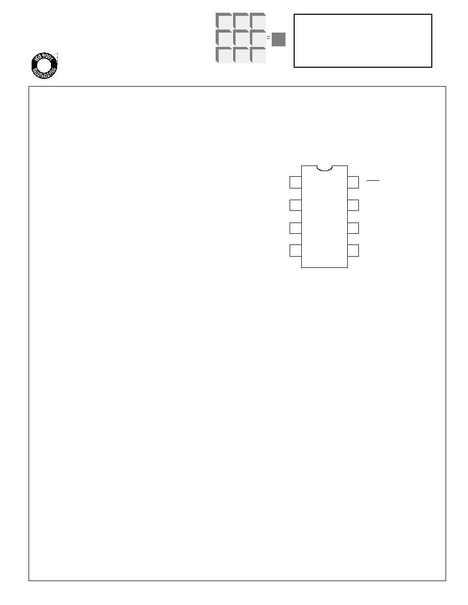
∑ LS7534, LS7535, LS7535FT (DIP); - See Figure 1
LS7534-S, LS7535-S, LS7535FT-S (SOIC)
DESCRIPTION:
LS7534 and LS7535 are MOS integrated circuits
that are designed for brightness control of in-
candescent lamps. The outputs of these ICs control
the brightness of a lamp by controlling the firing an-
gle of a triac connected in series with the lamp. All
internal timings are synchronized with the line fre-
quency by means of a built-in phase-lock loop cir-
cuit. The output occurs once every half-cycle of the
line frequency. Within the half-cycle, the output can
be positioned anywhere between 159∞ conduction
angle for maximum brightness and 41∞ conduction
angle for minimum brightness in relation to the AC
line frequency. The positioning of the output is con-
trolled by applying the proper logic levels at the UP
and DOWN inputs.
These functions may be implemented with very few
interface components which is described in the ap-
plication examples (See Fig. 5A and 5B). For touch
plates, LS7534 is used (Fig. 5A). For pushbutton
switches, LS7535 is used (Fig. 5B).
In the following Operating Description of the applica-
tion examples, an Activation is Touch for LS7534
and Switch Closure for LS7535.
Short Activation (34ms to 325ms)
UP - When the lamp is off, if a short activation is applied to
the UP input, the lamp brightness is ramped up to full-on or
to a previous brightness stored in the memory. The ramp-
up time from off to full-on is 2.8 sec. The ramp-up time from
off to any other brightness is
proportionally shorter. When
the lamp is on at any brightness, a short activation applied
to the UP input has no effect.
DOWN - If a short activation is applied to the DOWN input,
the lamp brightness is ramped down to off. The ramp-down
time from full-on to off is 5.6 seconds. The ramp-down time
from any other brightness is proportionally shorter. When
the lamp is off, a short activation applied to the DOWN input
has no effect.
Long Activation (Greater than 334ms)
UP - If a long activation is applied to the UP input, the lamp
brightness ramps up from the pre-activation brightness as
long as the activation is maintained or until the full bright-
ness is reached. At full brightness any continued long ac-
tivation has no further effect.
DOWN - If a long activation is applied to the DOWN input,
the lamp brightness is ramped down as long as the long ac-
tivation is maintained or until the minimum brightness is
reached. At minimum brightness, any continued long ac-
tivation has no further effect. When the lamp is off, a long
activation applied to the DOWN input has no effect.
PIN ASSIGNMENT - TOP VIEW
LSI
1
2
3
4
8
7
6
5
LS7534
FIGURE 1
TRIG
V
DD
(-V
)
DOWN
UP
V
SS
(+V)
DOZE
CAP
S Y N C
7535-060303-1
LSI/CSI
LSI Computer Systems, Inc. 1235 Walt Whitman Road, Melville, NY 11747 (631) 271-0400 FAX (631) 271-0405
UL
Æ
A3800
LS7534, LS7535
LS7535FT
June 2003
APPLICATION:
LS7535 is ideal for use in electronic dimmers for
"smart-house" type applications because it is designed
to be easily controlled by remote switches.
LS7535FT NOTE
LS7535FT ramp-up and ramp-down times are instantaneous.
Otherwise, it functions the same as LS7535.

UP/DOWN SIGNAL DURATION
SHORT LONG
INPUT 34ms to 325 ms More than 334ms
UP
DOWN
PRE-ACTIVATION
BRIGHTNESS
Off
Max.
Intermediate
Off
Max.
Intermediate
POST-ACTIVATION
BRIGHTNESS
Memory **
(See Note 1)
No Change
No Change
No Change
Off *
Off *
PRE-ACTIVATION
BRIGHTNESS
Off
Max.
Intermediate
Off
Max.
Intermediate
POST-ACTIVATION
BRIGHTNESS
Increases from Min.
No change
Increases from pre-
touch brightness
No change
Decreases from Max.
Decreases from pre-
touch brightness
* 5.6 second ramp-down from max. to off. Ramp-down time from any other brightness is proportionally shorter.
** 2.8 second ramp-up from off to max.
NOTE 1: "Memory" refers to the brightness stored in the memory. The brightness is stored in memory when the
lamp is turned off by a short activation. First time after power-up, a short activation produces max. brightness.
INPUT/OUTPUT DESCRIPTION:
V
SS
(Pin 1)
Supply voltage positive terminal.
DOZE (Pin 2)
A clock applied to this input causes the brightness to de-
crease in equal increments with each negative transition
of the clock. Eventually, when the lamp becomes off, this
input has no further effect. The lamp can be turned on
again by activating the UP input. For the transition from
maximum brightness to off, a total of 83 clock pulses are
needed at the DOZE input.
When either the UP or the DOWN input is active, the
DOZE input is disabled.
CAP (Pin 3)
The CAP input is for external component connection for
the PLL filter capacitor. A capacitor of 0.047µF ± 20%
should be used at this input.
SYNC (Pin 4)
The AC line frequency (50Hz/60Hz), when applied to this
input, synchronizes all internal timings through a phase
lock loop. The signal for this input may be obtained from
the line voltage by employing the circuit arrangement
shown in the application examples.
UP (Pin 5)
This input controls the turn-on and the conduction angle,
¯ ,
of the TRIG output. A description of this is provided in the
DESCRIPTION and TABLE 1. For LS7534, a logic low level
is the active level whereas for LS7535 a logic high level is
the active level. LS7535 has an internal pull-down resistor
of about 500k Ohms on this input.
DOWN (Pin 6)
This input controls the turn-off and the conduction angle, ¯,
of the TRIG output. A description of this is provided in the
DESCRIPTION and TABLE 1. For LS7534, a logic low level
is the active level, whereas for LS7535 a logic high level is
the active level. LS7535 has an internal pull-down resistor
of about 500k Ohms on this input.
V
DD
(Pin 7)
Supply voltage negative terminal.
TRIG (Pin 8)
The TRIG output provides a low level pulse occurring every
half-cycle of the SYNC signal. The conduction angle,
¯,
of
the TRIG output can be varied within the range of 41o to
159o by means of either the UP or the DOWN input.
TABLE 1
7535-012703-2

ABSOLUTE MAXIMUM RATINGS:
PARAMETER
SYMBOL
VALUE
UNIT
DC supply voltage
V
SS -
V
DD
+20
V
Any input voltage
V
IN
V
SS
- 20 to V
SS
+ 0.5
V
Operating temperature
T
A
0 to +80
∞C
Storage temperature
T
STG
-65 to +150
∞C
DC ELECTRICAL CHARACTERISTICS:
(T
A
= 25∞C, all voltages referenced to V
DD
)
PARAMETER
SYMBOL
MIN
TYP
MAX
UNIT
CONDITIONS
Supply voltage
V
SS
+12
-
+18
V
-
Supply current
I
SS
-
1.2
1.7
mA
V
SS
= +15V,
Output off
Input Voltages:
DOZE LO
V
IZL
0
-
V
SS
- 6
V
-
DOZE HI
V
IZH
V
SS
- 2
-
V
SS
V
-
SYNC LO
V
IRL
0
-
V
SS
- 9.5
V
-
SYNC HI
V
IRH
V
SS
- 5.5
-
V
SS
V
-
UP, DOWN LO
V
IOL
0
-
V
SS
- 8
V
-
UP, DOWN HI
V
IOH
V
SS
- 2
-
V
SS
V
-
Input Current:
SYNC, UP, DOWN HI
I
IH
-
-
110
uA
With Series 1.5M
Resistor to
115 VAC Line
SYNC, UP, DOWN LO
I
IL
-
-
100
nA
-
DOZE HI
I
IH
-
-
100
nA
-
DOZE LO
I
IL
-
-
100
nA
-
TRIG HI
V
OH
-
V
SS
-
V
-
TRIG LO
V
OL
-
V
SS
- 8
-
V
V
SS
= +15V
TRIG Sink Current
I
OS
50
-
-
mA
V
SS
= +15V,
V
OL
= V
SS
- 4V
TRANSIENT CHARACTERISTICS (See Fig. 2 and 3)
(All timings are based on fs = 60Hz, unless otherwise specified.)
PARAMETER
SYMBOL
MIN
TYP
MAX
UNIT
SYNC frequency
fs
40
-
70
Hz
UP, DOWN duration (SHORT)
Ts
1
34
-
325
ms
UP, DOWN duration (LONG)
Ts
2
334
-
infinite
ms
¯
ramp time, off to max
T
US
-
2.8
-
sec
(UP,SHORT)
¯
ramp time, min to max
T
UL
-
3.6
-
sec
(UP,LONG)
¯
ramp time, max to min
T
DS
-
5.6
-
sec
(DOWN,SHORT)
¯
ramp time, max to min
T
DL
-
3.6
-
sec
(DOWN,LONG)
TRIG pulse width
T
W
-
33
-
µs
TRIG conduction angle (See Note)
¯
41
-
159
degrees
DOZE frequency
f
D
0
-
500
Hz
NOTE: The phase delay caused by the typical RC network used between SYNC input and the AC line (See Fig. 5A and
Fig. 5B) reduces the effective ¯ values by 8∞.
7535-012703-3

FIGURE 3. OUTPUT CONDUCTION ANGLE,
¯
, vs UP/DOWN INPUTS
Note 1. UP/DOWN input polarity shown is for LS7534. For LS7535, the polarity is reversed.
Note 2. Points A, D, E and K correspond to minimum brightness, where ¯ = 41∞.
Points B, C, G and H correspond to maximum brightness, where ¯ = 159∞.
Points denoted by M correspond to an arbitrary intermediate brightness.
Note 3. Points F, J and L correspond to ¯ = 64∞. The ramp-up or ramp-down rate of ¯ changes at these points
(upon long activation only) indicated by the discontinuity of the slopes. The interval E to F or J to K,
in terms of time and angle, are 934ms and 23∞, respectively.
OUT
¯
SYNC
T
W
T
W
200
150
100
50
0
DOWN
UP
(Degrees)
0
4
8
12
16
0
4
8
12
0
4
8
12
16
20
24
A
B
C
D
E
F
H
K
G
J
M
L
M
T
DL
334ms
334ms
T
S2
T
S2
T
S1
T
S2
T
S1
T
S1
T
S1
T
US
T
DS
T
UL
334ms
¯
SECONDS
FIGURE 2. OUTPUT CONDUCTION ANGLE,
¯
7535-012703-4

TRIG
OUTPUT
DRIVER
DIGITAL
COM-
PARATOR
BRIGHTNESS
MEMORY
ÿ
POINTER
PHASE
LOCK
LOOP
CONTROL
LOGIC
BUF
BUF
BUF
BUF
SYNC
CAP
DOZE
DOWN
UP
(+V)
(-V)
FIGURE 4
L S 7 5 3 4 / L S 7 5 3 5 B L O C K D I A G R A M
4
3
2
6
5
1
7
8
V
SS
V
DD
APPLICATION EXAMPLES:
Typical dimmer light switch circuit schematics are shown in Fig. 5A (LS7534) and
Fig. 5B (LS7535). The brightness of the lamp is set by touching the UP and DOWN
touch plates in Fig. 5A and closure of the UP and DOWN switches in Fig. 5B. The
functions of different components are as follows:
∑ Z, D1, R1, C2 and C5 produce the 15V DC supply for the chip.
∑ R2
and C4
filter and current limit the AC signal for the SYNC input.
∑ C3 is the filter capacitor for the internal PLL.
∑ C1 and L are RFI filters.
∑ In Fig. 5A, R3 and R4 set the touch sensitivity of the UP and DOWN inputs.
∑ In Fig. 5B, R3 limits the current between Vss and the UP and DOWN inputs upon
closure of a switch.
∑ The resistor and diode connected between the chip output and the triac gate
provides current limiting and isolation for the chip. The resistor is R5 in Fig. 5A
and R4 in Fig. 5B.
∑ In Fig. 5B, PCB layout may cause triac switching transients to be coupled to the Up
or Down input which can have the effect of having a Long switch closure "lock-up"
at a certain phase angle output. In this case, capacitors C6 and C7 must be added
as shown.
The information included herein is believed to be
accurate and reliable. However, LSI Computer Systems,
Inc. assumes no responsibilities for inaccuracies, nor for
any infringements of patent rights of others which may
result from its use.
7535-012703-5