
80C03
4-1
MD400121/C
1
80C03
AutoDUPLEX
TM
CMOS Ethernet
Data Link Controller
Features
s
Low Power CMOS Technology
s
Optimized for Embedded Ethernet Applications
s
Meets ANSI/IEEE 802.3 and ISO 8802-3 Standards
for Ethernet (10Base-5) Thin Net (10Base-2)
(10Base-T) and Twisted Pair
s
10 MHz Serial/Parallel Conversion
s
Preamble Generation and Removal
s
Automatic 32-Bit FCS (CRC) Generation and
Checking
s
Collision Handling, Transmission Deferral and
Retransmission with Automatic Jam and
Backoff Functions
s
Error Interrupt and Status Generation
s
Available as "Ethernet Core" for Custom ASIC
Applications
s
Single 5 V
�
10% Power Supply
s
Standard CPU and Peripheral Interface
Control Signals
s
Loopback Capability for Diagnostics
s
Single Phase Clock
s
Inputs and Outputs TTL Compatible
Functional Block Diagram
96253
s
Compatible with SEEQ 8003 and Provides
Additional Features
- 64 bit Multicast Filter
- Transmit Collision Counter
- Total Collision Counter
- Reports Status of "Carrier" and "SQE" During
Transmits
- Transmit No CRC Mode
- Transmit No Preamble Mode
- Transmit Packet Autopadding Mode
- Receive CRC Mode
- Receive Own Transmit Disable Mode
- Group Address Mode
- Fast Receive Discard Mode
- Full Duplex Mode
s
Supports AutoDUPLEX Mode for Automatic Full
Duplex Operation-- Provides 20 MBits/sec
Bandwidth for Switched Networks
s
40 Pin DIP Package, 44 Pin PLCC
AutoDUPLEX is a trademark of SEEQ Technology Inc.
ENCODER
INTERFACE
DATA
INTERFACE
RxTxD (0 � 7)
RxRDY
16-BYTE
RECEIVE
FIFO
RECEIVE
COUNTER
CSN
RxC
DECODER
INTERFACE
SERIAL
/PARALLEL
PARALLEL
/SERIAL
16-BYTE
TRANSMIT
FIFO
CRC
STRIPPER
CRC
CHECKER
ADDRESS
CHECKER
RECEIVE BIT
CONTROL
PLA
RECEIVE
BYTE
CONTROL
CLOCK
DRIVERS
RxD
TxC
RESET
CONTROL
REGISTER
FILE
A2
A1
A0
INT
R x DC
T x RET
COMMAND/
STATUS
INTERFACE
M
U
X
INTERRUPT
AND
CONTROL
CdSt (0 � 7)
WR
RD
CS
TxD
COLL
TxEN
TRANSMIT
BYTE
CONTROL
TRANSMIT
BYTE
COUNTER
ATTEMPT
COUNTER
BACKOFF
CONTROLLER
CRC
GENERATOR
TxRDY
RxRD
RxTxEOF
TxWR
Note: Check for latest Data Sheet revision
before starting any designs.
SEEQ Data Sheets are now on the Web, at
www.lsilogic.com.
This document is an LSI Logic document. Any
reference to SEEQ Technology should be
considered LSI Logic.
80C03
4-2
MD400121/C
2
Description
The SEEQ Ethernet Data Link Controller (EDLC
�
) is
designed to support Data Link Layer (layer 2) of the
Ethernet specification for Local Area Networks (LAN). The
system interface is optimized for ease of connection to
commonly available DMA Controllers and specifically for
BURST MODE OPERATION. The 80C03 interfaces di-
rectly to the 8023A and 8020 Manchester Code Convert-
ers (MCC
TM
) to complete the station resident Ethernet
functions. The protocol used is Carrier Sense, Multiple
Access with Collision Detection (CSMA/CD). The 80C03
EDLC chip is a single VLSI device which is designed to
greatly simplify the development of Ethernet communica-
tion in computer based systems. The 80C03 provides an
economic solution for the construction of an Ethernet
node, providing high speed data communication at 10
Megabits/second and sees applications in terminals,
workstations, personal computers, small business sys-
tems, and large computer systems, in both the office and
industrial environment. The 80C03 EDLC chip has a
universal system interface compatible with almost any
microprocessor, microcomputer, or system bus, allowing
the system designer to make the price/performance
tradeoffs for each application. The transmit and receive
sections of the EDLC chip are independent and can
operate simultaneously to allow reception of a transmitted
frame for use in loopback diagnostics modes.
The 80C03 is compatible with SEEQ 8003 and provides
additional programmable features. The features enabled
on demand are: 64 bit Multicast filter, Transmit Collision
Counter, Total Collision Counter, Status Reporting of
Carrier and SQE during transmits, Transmit no CRC,
Transmit no Preamble, Transmit Packet Autopadding,
Receive CRC, Receive Own Transmit disable, Receive
Group Address mode, Fast Receive Discard Mode, and
Full Duplex Mode.
Functional Description
Frame Format
On an Ethernet communication network, information is
transmitted and received in packets or frames. An Eth-
ernet frame consists of a preamble, two address fields, a
byte-count field, a data field and a frame check sequence
(FCS). Each field has a specific format which is described
in detail below. An Ethernet frame has a minimum length
of 64 bytes and a maximum length of 1518 bytes exclusive
of the preamble. The Ethernet frame format is shown
below.
NOTE:
Field length in bytes in parentheses.
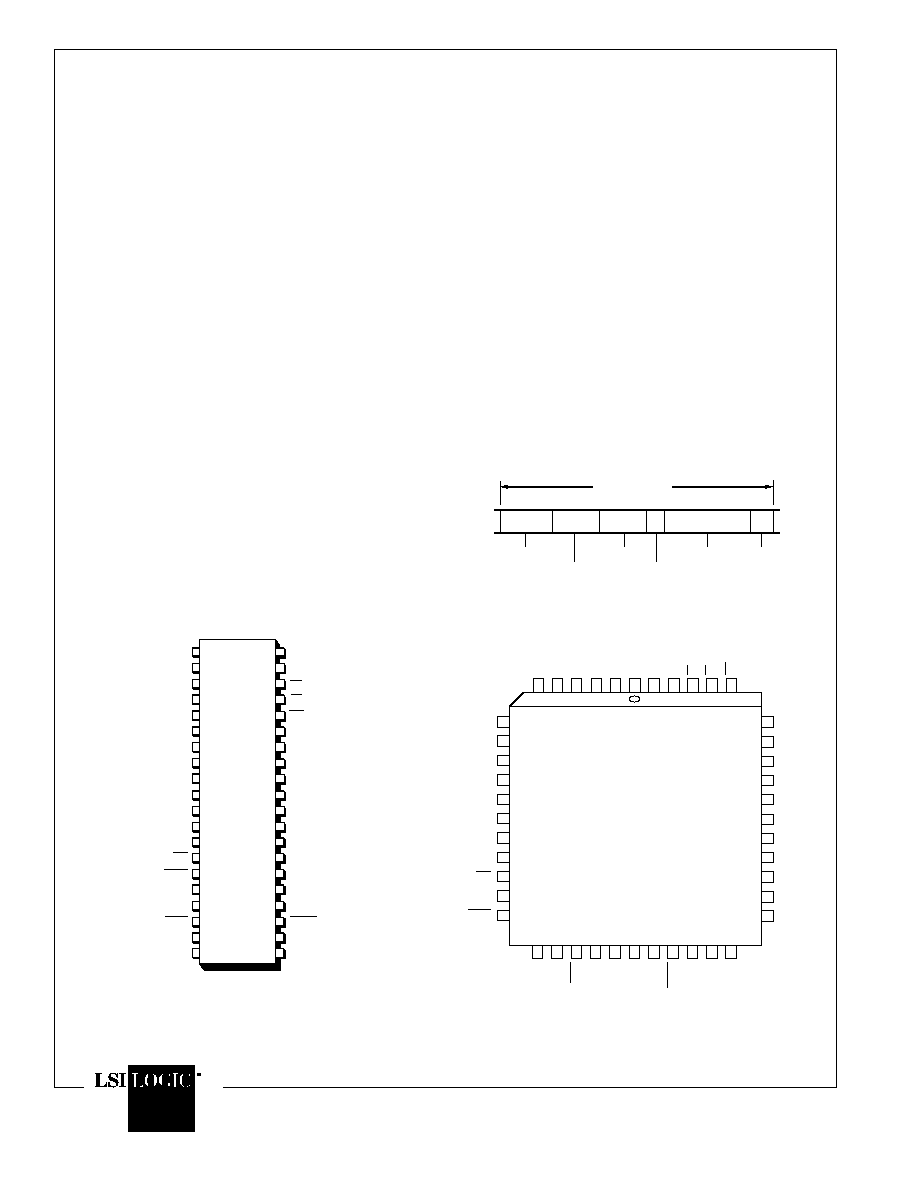
Figure 1. Dual-In-Line
Top View
MCC is a trademarks of SEEQ Technology Inc.
EDLC is a registered trademark of SEEQ Technology Inc.
Figure 2. Plastic Leaded Chip Carrier
Top view
6
5
4
3
2
1
44
43
42
41
40
7
8
9
10
11
12
13
14
15
16
17
18
19
20
21
22
23
24
25
26
27
28
39
38
37
36
35
34
33
32
31
30
29
CdSt 1
CdSt 0
CdSt 2
CdSt 3
CdSt 4
CdSt 5
CdSt 6
CdSt 7
RxC
ADUPLX*
RxTx D0
TxRET
TxD
TxEN
A0
A1
CC
V
A2
WR
RD
CS
VSS
TxRDY
RxTx EOF
RxRDY
RxD
CSN
INT
RxDC
COLL
RxRD
RESET
V
SS
RxTxD5
RxTxD3
RxTxD7
TxWR
RxTxD4
RxTxD6
RxTxD2
RxTxD1
TxC
VSS
V
SS
A1
A0
TxEN
TxD
1
2
3
4
5
6
7
8
9
10
11
12
40
39
38
37
36
35
34
33
32
31
30
29
VCC
A2
WR
RD
13
14
15
16
17
18
19
20
28
27
26
25
24
23
22
21
VSS
TxRET
RxTxD0
RxTxD1
RxTxD2
RxTxD3
RxTxD4
RxTxD5
RxTxD6
RxTxD7
TxC
TxWR
TxRDY
RxTxEOF
RxRD
RxRDY
CdSt0
CdSt1
CdSt2
CdSt3
CdSt4
CdSt5
CdSt6
CdSt7
CS
RxC
RxD
CSN
INT
COLL
RESET
RxDC
PREAMBLE
(8)
DESTINATION
ADDRESS
(6)
SOURCE
ADDRESS
(6)
BYTE
COUNT
(2)
DATA
(46-1500)
FCS
(4)
ETHERNET FRAME

80C03
4-3
MD400121/C
3
FIRST BYTE
LAST BYTE
DESTINATION
ADDRESS
(6 BYTES)
SOURCE
ADDRESS
(6 BYTES)
BYTE COUNT
(2 BYTES)
DATA
(46 � 1500
BYTES)
A7
A15
A23
A31
A39
A47
B7
B15
B23
B31
B39
B47
T7
T15
D7
A0
A8
A16
A24
A32
A40
B0
B8
B16
B24
B32
B40
T0
T8
D0
. . . . . .
. . . . . .
. . . . . .
. . . . . .
. . . . . .
. . . . . .
. . . . . .
. . . . . .
. . . . . .
. . . . . .
. . . . . .
. . . . . .
. . . . . .
. . . . . .
. . . . . .
Figure 3. Typical Frame Buffer Format for
Byte-Organized Memory
EDLC chip encapsulates these fields into an Ethernet
frame by inserting a preamble prior to these information
fields and appending a CRC after the information fields.
The chip can be programmed to exclude inclusion of the
preamble and/or the FCS from the transmit data stream. In
this case it is assumed that the preamble and FCS are
provided as part of the data written to the chip.
Transmission Initiation/Deferral
The Ethernet node initiates a transmission by storing the
entire information content of the frame to be transmitted in
an external buffer memory, and then transferring initial
frame bytes to the EDLC Transmit FIFO. "Transmit-buffer
to FIFO" transfers are coordinated via the TxWR and
TxRDY handshake interface, i.e., bytes are written to the
BIT
NAME
PIN
NO.
RxTxD0
RxTxD1
RxTxD2
RxTxD3
RxTxD4
RxTxD5
RxTxD6
RxTxD7
6
7
8
9
10
11
12
13
PREAMBLE
FIRST BYTE
SIXTH BYTE
A0 . . . A7
A8 . . . A15
. . . . . .
A40 . . . A47
SOURCE ADDRESS . . .
DESTINATION ADDRESS
BITS WITHIN A BYTE TRANSMITTED/RECEIVED BIT NO. "0" FIRST THROUGH BIT NO. "7" LAST.
. . .
Preamble: The preamble is a 64-bit field consisting of 62
alternating "1"s and "0"s followed by a "11" End-of-Pre-
amble indicator.
Destination Address: The Destination Address is a 6-
byte field containing either a specific Station Address, a
Broadcast Address, or a Multicast Address to which this
frame is directed.
Source Address: The Source Address is a 6-byte field
containing the specific Station Address from which this
frame originated.
Byte-Count Field: The Byte-Count Field consists of two
bytes providing the number of valid data bytes in the Data
Field, 46 to 1500. This field is uninterpreted at the Data
Link Layer, and is passed through the EDLC chip to be
handled at the Client Layer.
Data Field: The Data Field consists of 46 to 1500 bytes of
information which are fully transparent in the sense that
any arbitrary sequence of bytes may occur.
Frame Check Sequence: The Frame Check Sequence
(FCS) field is a 32-bit cyclic redundancy check (CRC)
value computed as a function of the Destination Address
Field, Source Address Field, Type Field and Data Field.
The FCS is appended to each transmitted frame, and used
at reception to determine if the received frame is valid.
Transmitting
The transmit data stream consists of the Preamble, four
information fields, and the FCS which is computed in real
time by the EDLC chip and automatically appended to the
frame at the end of the serial data. The Preamble is also
generated by the EDLC chip and transmitted immediately
prior to the Destination Address. Destination Address,
Source Address, Type Field and Data Field are prepared
in the buffer memory prior to initiating transmission. The
Figure 4. Bit Serialization/Deserialization

80C03
4-4
MD400121/C
4
FIFO via TxWR only when TxRDY is HIGH. Actual
transmission of the data onto the network will only occur if
the network has not been busy for the minimum defer time
(9.6
�
s) and any Backoff time requirements have been
satisfied. When transmission begins, the EDLC chip
activates the transmit enable (TxEN) line concurrently with
the transmission of the first bit of the Preamble and keeps
it active for the duration of the transmission.
Collision
When concurrent transmissions from two or more Eth-
ernet nodes occur (collision), the EDLC chip halts the
transmission of the data bytes in the Transmit FIFO and
transmits a Jam pattern consisting of 55555555 hex. At
the end of the Jam transmission, the EDLC chip issues a
TxRET signal to the CPU and begins the Backoff wait
period.
To reinitiate transmission, the initial bytes of the frame
information fields must be reloaded into the EDLC Trans-
mit FIFO. The TxRET is used to indicate to the buffer
manager the need for frame reinitialization. The reloading
of the Transmit FIFO may be done prior to the Backoff
interval elapsing, so that no additional delay need be
incurred to retransmission.
Scheduling of retransmission is determined by a con-
trolled randomization process called Truncated Binary
Exponential Backoff. The EDLC chip waits a random
interval between 0 and 2
K
slot times (51.2
�
s per slot time)
before attempting retransmission, where "K" is the current
transmission attempt number (not to exceed 10).
When 16 consecutive attempts have been made at trans-
mission and all have been terminated due to collision, the
EDLC Transmit Control sets an error status bit and issues
an interrupt to the CPU if enabled.
Terminating Transmission
Transmission Terminates under the following conditions:
Normal: The frame has been transmitted successfully
without contention. Loading of the last data byte into the
Transmit FIFO is signaled to the EDLC chip by activation
of the RxTxEOF signal concurrently with the last byte of
data loaded into the Transmit FIFO. This line acts as a
ninth bit in the Transmit FIFO. When this last byte is
serialized, if the chip is not in Transmit No CRC mode, then
the CRC is appended and transmitted concluding frame
transmission. The Transmission Successful bit of the
Transmit Status Register will be set by a normal termina-
tion.
Collision: Transmission attempted by two or more Eth-
ernet nodes. The Jam sequence is transmitted, the Colli-
sion status bit is set, transmit Collision Counter is updated,
the TxRET signal is generated, and the Backoff interval
begun.
Underflow: Transmit data is not ready when needed for
transmission. Once transmission has begun, the EDLC
chip on average requires one transmit byte every 800 ns
in order to avoid Transmit FIFO underflow (starvation). If
this condition occurs, the EDLC chip terminates the trans-
mission, issues a TxRET signal, and sets the Transmit-
Underflow status bit.
16 Transmission Attempts: If a Collision occurs for the
sixteenth consecutive time, the 16-Transmission-At-
tempts status bit is set, the Collision status bit is set, the
TxRET signal is generated, and the Backoff interval be-
gun. The counter that keeps track of the number of
collisions is modulo 16 and therefore rolls over on the 17th
collision. Bits 15 to 11 on the Collision Count Registers
(80C03 mode) indicates the attempt counter used for
Collision back-off. These can be read and cleared as
described in the Transmit Command register description.
At the completion of every transmission or retransmission,
new status information is loaded into the Transmit Status
Register. Dependent upon the bits enabled in the Trans-
mit Command Register, an interrupt will be generated for
the just completed transmission. In both collision and
underflow the TxRET signal is activated.
Receiving
The EDLC chip is continuously monitoring the network.
When activity is recognized via the Carrier Sense (CSN)
line going active, the EDLC chip synchronizes itself to the
incoming data stream during the Preamble, and then
examines the destination address field of the frame. De-
pending on the Address Match Mode specified, the EDLC
chip will either recognize the frame as being addressed to
itself in a general or specific fashion or abort the frame
reception. The 80C03 also allows counting of all collisions
seen on the network.
Preamble Processing
The EDLC chip recognizes activity on the Ethernet via the
Carrier Sense line. The Preamble is normally 64 bits (8
bytes) long. The Preamble consists of a sequence of 62
alternating "1"s and "0"s followed by "11", with the frame
information fields immediately following. In order for the
decoder phase-lock to occur, the EDLC chip waits 16 bit
times before looking for the "11" end of preamble indicator.
If the EDLC chip receives a "00" before receiving the "11"
in the Preamble, an error condition has occurred. The
frame is not received, and the EDLC chip begins monitor-
ing the network for a carrier again.

80C03
4-5
MD400121/C
5
TRANSMIT
RECEIVE
DATA
BUFFER
BUS
TRANSCEIVER
DMA/
BUFFER
CONTROL
CPU
SYSTEM
MEMORY
80C03
EDLC
8020 or 8023
MANCHESTER
CODE
CONVERTER (MCC)
COLLISION
TRANSMIT
RECEIVE
TO 83C92 CMOS COAX TRANSCEIVER
83C94 CMOS TWISTED PAIR TRANSCEIVER
Figure 5. Typical Ethernet Node Configuration
Address Matching
Ethernet addresses consist of two 6-byte fields. The first
bit of the address signifies whether it is a Station Address
or a Multicast/Broadcast Address.
mine which byte is selected and bits 3 thru 5 to determine
which bit according to the following tables:
FCS Bits
Byte Selected
0 1 2
0 0 0
Byte 0
0 0 1
Byte 1
0 1 0
Byte 2
0 1 1
Byte 3
1 1 1
Byte 7
FCS Bits
Bit Selected
4 5 6
0 0 0
Bit 0
0 0 1
Bit 1
0 1 0
Bit 2
0 1 1
Bit 3
1 1 1
Bit 7
Multicast Address: If the first bit of the incoming address
is a 1 and the EDLC chip is programmed to accept
Multicast Addresses without using Hash filtering, the
frame is received. The 80C03 also can be programmed to
use hash filter for determining acceptance of multicast
addresses.
First Bit
Address
0
Station Address (Physical)
1
Multicast/Broadcast Address
(logical)
Address matching occurs as follows:
Station Address: All destination address bytes must
match the corresponding bytes found in the Station Ad-
dress Register. If Group Address mode is enabled, the last
4 bits of the station address are masked out during address
matching.
After computing the FCS on the first six bytes of the
address field (Destination address), the 80C03 uses bits 0
thru 5 as an address to the Multi-cast address filter
register. Bit 0 of the FCS is assumed to be where receive
data enters the FCS generation circuitry. If the corre-
sponding bit addressed in the Multicast address filter
register is a `1' the 80C03 will receive the frame, otherwise
it will discard the frame. Addressing of the Multicast
address filter register occurs using bits 0 thru 2 to deter-