 | –≠–ª–µ–∫—Ç—Ä–æ–Ω–Ω—ã–π –∫–æ–º–ø–æ–Ω–µ–Ω—Ç: 80C25 | –°–∫–∞—á–∞—Ç—å:  PDF PDF  ZIP ZIP |
80C25
1
MD400142/D
80C25
96345
MCC and AutoDUPLEX are trademarks of SEEQ Technology, Inc.
Pin Configuration
Functional Features
s
Low Power CMOS Technology Ethernet Serial
Interface Adapter with Integrated Manchester
Code Converter (MCC
TM
), AUI and 10Base-T
Transceiver with Output Wave Shaping and on
chip filters.
s
Meets IEEE 802.3 10Base-5, 10Base-2, 10Base-T
Standards
s
Direct Interface to SEEQ & INTEL Controllers,
See the 80C26 Data Sheet for Direct Interface to
AMD and NSC Controllers
s
Automatic or Manual Selection of AUI/10Base-T
Interface
s
Provides AutoDUPLEX
TM
Detect Function for
SEEQ LAN Controllers, Doubling Bandwidth
to 20 MBits/sec for Switched Networks
s
Separate Analog/Digital Power and Ground Pins
to Minimize Noise
Interface Features
s
Meets IEEE 10Base-T Standards and IEEE 802.3
standards for AUI.
s
On Chip Transmit Wave Shaping and Low Pass
Filter Circuits - No External Filters Required
s
Link Integrity Test Disable, Selectable Coded
Link Pulse for AutoDUPLEX Mode
s
Automatic Polarity Correction
s
Low differential and common mode noise on TP
transmit outputs.
s
Differential Transmit Drivers to support 50 Meters
of AUI Cable Lengths.
s
Direct AUI interface to the Manchester Code
Converter.
General Description
The SEEQ 80C25 is a CMOS single chip Ethernet serial
interface adapter with a integrated Manchester Code
Converter (MCC), AUI & 10Base-T transceiver with wave
shaping & filters eliminating the need for external filters.
The 80C25 is designed to interface directly with SEEQ and
Intel Ethernet data link controllers. The chip provides
automatic polarity correction, automatic port selection,
separate analog & digital ground pins & a link disable
feature. It also provides a selectable coded link pulse to
implement AutoDUPLEX function together with SEEQ
family of controllers allowing seamless full duplex opera-
tion in switched network implementations doubling net-
work bandwidth to 20 Mbps in 10Base-T. The 80C25 is
typically suitable for adapter boards, motherboards and
stand-alone TP transceiver designs & switching hubs.
5
6
7
8
9
10
11
CSN
DI ≠
LNK_LED/LNK_DIS
FDPLX_DET
CI +
DO ≠
DI +
CI ≠
2
1
28
27
26
3
CIS
TP/AUI
4
DO +
GND
1
V
CC1
25
24
23
22
21
20
19
TPO ≠
TPO +
TPI ≠
TXEN
TPI +
RXD
TXD
TXC
12
13
14
15
16
17
18
X1
RXC
REXT
FDPLX
COL
GND
2
V
CC2
28 Pin PLCC
Top View
Full Duplex
AutoDUPLEX
TM
CMOS Ethernet Interface Adapter
in 28L Package
Note: Check for latest Data Sheet revision
before starting any designs.
SEEQ Data Sheets are now on the Web, at
www.lsilogic.com.
This document is an LSI Logic document. Any
reference to SEEQ Technology should be
considered LSI Logic.
80C25
2
MD400142/D
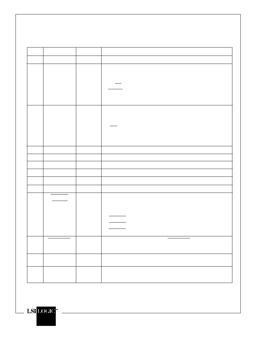
Pin
Name
I/O
Description
1
V
CC1
--
Power Supply. +5 Volts.
2
TP/AUI
I
TP or AUI or Autoport Select Input. This pin selects the
Pullup To
interface to the ENDEC. This pin is a three state input that is
V
CC
/2
internally biased at V
CC
/2.
TP/AUI
1
TP Port
float
Autoport
0
AUI Port
3
CIS
I
Controller Interface Select Input.
Pulldown
CIS
0
SEEQ
1
Intel
The 80C26 Provides interface to NSC and AMD Controllers.
4
DO +
O
AUI Transmit Output, Positive.
5
DO ≠
O
AUI Transmit Output, Negative.
6
CI +
I
AUI Collision Input, Positive.
7
CI ≠
I
AUI Collision Input, Negative.
8
DI +
I
AUI Receive Input, Positive.
9
DI ≠
I
AUI Receive Input, Negative.
10
LNK_LED
I/O
Link Detect Output and Link Disable Input. This pin consists of an
/LNK_DIS
LNK_LED = 1
Output
Link Pulse Not Detected
LNK_LED = 0
Output
Link Pulse Detected
LNK_LED = D
GND
Input
Link Test Function Disabled
11
FDPLX_DET
O
Full Duplex Detect Output. When FDPLX_DET = 0, the device
has been placed in the full duplex mode by either selection or by
the AutoDUPLEX feature.
12
CSN
O
Carrier Sense Output. This controller interface output indicates
valid data and collisions on the receive TP or AUI inputs.
13
TXC
O
Transmit Clock Output. This controller interface output provides
a 10 MHz clock to the controller. Transmit data from the controller on
TXD is clocked in on edges of TXC.
80C25 Pin Description
open drain output transistor. If the pin is tied to D
GND
, the link test
function is disabled. Otherwise, the pin is a Link Pulse Detect output
and can drive an LED.
80C25
3
MD400142/D
14
COL
O
Collision Output. This controller interface output is asserted
when collision transmit and receive data occurs and during SQE test.
15
V
CC2
--
Power Supply. +5 Volts.
16
GND
2
--
Ground. 0 Volts.
17
X1
I
Crystal Oscillator Input. The master clock for the device is
generated by either placing a crystal between X1 and DGND, or
by applying an external clock to X1.
If a crystal is used as the clock source, connect a 1M
resistor
between X1 and GND. For external oscillator operation, connect a
470
resistor in series between X1 and clock source.
18
RXC
O
Receive Clock Output. This controller interface output provides
a 10 MHz clock to the controller. Receive data on RXD is clocked
out on edges of RXC.
19
RXD
O
Receive Data Output. This controller interface output contains
receive data decoded from the receive TP/AUI inputs and is
clock out on edges of RXC.
20
TXD
I
Transmit Data Input. This controller interface input contains data
to be transmitted on either TP or AUI transmit outputs and is clocked
in on edges of TXC.
21
TXEN
I
Transmit Enable Input. This controller interface input has to be
asserted when data on TXD is valid.
22
TPI≠
I
Twisted Pair Receive Input, Negative.
23
TPI+
I
Twisted Pair Receive Input, Positive.
24
TPO≠
O
Twisted Pair Transmit Output, Negative.
25
TPO+
O
Twisted Pair Transmit Output, Positive.
26
REXT
--
Transmit Current Set. An external resistor tied between this pin
and A
GND
sets the twisted pair transmit output current level on TPO
±
.
27
FDPLX
I
Full Duplex/AutoDUPLEX Mode Select Input. This pin is a three
Pullup to
state input that is internally biased to V
CC
/2.
V
CC
/2
FDPLX
1
Full Duplex Mode
float
AutoDUPLEX Mode
0
Normal
28
GND
1
--
Ground. 0 Volts.
Pin
Name
I/O
Description
Pin Description
cont'd

80C25
4
MD400142/D
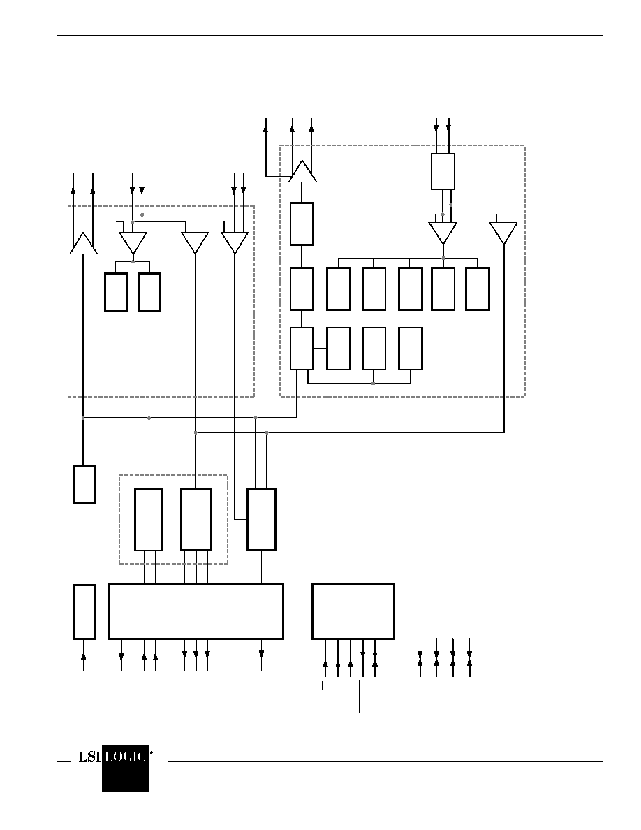
BLOCK DESCRIPTION
Functional Description
The 80C25 is an Ethernet adapter with a integrated Man-
chester Code Converter, 10Base-T transceiver with on
chip filters. The device contains both 10Base-T and AUI
interfaces compliant with IEEE 802.3 specifications. The
chip is divided into four major blocks, namely (i) The
controller interface (ii) The Encoder / Decoder (iii) The
twisted pair interface and (iv) The AUI. The input signals
are received on the TP or AUI receivers depending on
which is selected. Both the twisted pair and AUI receivers
contain a threshold comparator to validate the signal and
a zero crossing comparator for checking the transitions.
Then the data is sent to the PLL in the decoder to separate
the data from the clock. On the other side, digital transmit
data is clocked into the device via the controller interface.
The data is then sent to the Manchester encoder to be
encoded. Encoded data is then transmitted on the twisted
pair or AUI based on the selected port.
The Controller Interface
The 80C25 is designed to interface directly to all of SEEQ's
Ethernet controllers, and INTEL's 82586/596/592/593
LAN controllers, with the use of CIS Pin. The controller
interface consists of the Transmit/Receive data (TXD/
RXD), transmit/receive Clocks (TXC/RXC), the Transmit
Enable (TXEN) input, the collision output (COLL), the Full
Duplex acknowledgment (FDPLX_DET) and the Carrier
Sense Output (CSN) pins. On the transmit side, data on
TXD is clocked into the device on the edges of TXC clock
output only when the data valid signal (TXEN) is asserted.
On the receive side, data on RXD is clocked out on edges
of RXC. In the SEEQ mode, RXC follows TXC for 1.5
µ
s
and then switches to the recovered clock. In the Intel
mode, RXC is held low for 1.5
µ
s while the PLL is acquiring
lock and then switches to the recovered lock. The
FDPLX_DET pin signifies to the controller that full duplex
channels have been established.
The Encoder/Decoder
Manchester encoding is a process of combining the clock
& the data stream together so that they can be transmitted
on the twisted pair interface or AUI at the transceiver side.
Once encoded, the first half contains the complement of
the data and the second half contains the true data, so that
a transition is always guaranteed at the middle of a bit cell.
Data encoding and transmission begins with TXEN going
active, and the subsequent data is clocked on the edges
of TXC and then gets encoded. The end of a transmit
packet occurs at a bit cell center if the last bit is a "ONE" or
at a bit boundary if the last bit is a "ZERO".
The decoding is a process of recovering the encoded data
stream coming from the receiver side and decoding it back
into the clock and data outputs using the phase locked loop
technique. The PLL is designed to lock into the preamble
of the incoming signal at less than 15 bit times with a
maximum jitter of
±
13.5 ns at the TPI or AUI inputs and can
also sample the incoming data with this amount of jitter.
The ENDEC asserts the CSN signal to indicate to the
controller that the data and clock received are valid and
available. There is an inhibit period after the end of a frame
after a node has finished transmitting for 4.4
µ
s during
which CSN is deasserted irregardless of the state of the
receiver and collision status.
Twisted Pair Interface
(a) The transmitter function
The transmitter transfers Manchester encoded data from
the ENDEC to the twisted pair cable. The circuit consists
of a set of functional blocks to provide pre-coded wave-
shaped, pre-equalized and smoothed waveforms so that
the outputs are made to appear as though it had passed
through a 5-7th order external elliptic passive filter, thereby
eliminating the need for an external filter. The waveform
generator consists of a ROM, DAC, PLL, filter and a output
driver to preshape the output waveform transmitted onto
the twisted pair cable to meet the pulse template require-
ments outlined in IEEE STD 802.3 and illustrated in figure
12. The DAC first converts the data pulse into a stair
stepped representation of the desired output waveform,
which goes through a second order low-pass filter. The
DAC values are determined from the ROM addresses,
which are chosen to have different values for long and
short data bits so as to shape the pulse to meet the
10Base-T waveform template. The line driver takes the
smoothed current waveform and converts it into an high
current output that can drive the TP directly without any
external filters. The current output is guaranteed to have a
The 80C25 supports SEEQ and INTEL Controllers
according to Table 1.
Table 1. CIS Pin Description
CIS
Controller Interface
0
SEEQ
1
INTEL
80C25
5
MD400142/D
MANCHESTER
ENCODER
X1
OSCILLATOR
TXC
TXD
TXEN
RXC
RXD
CSN
COLLISION
DETECT
COLL
TRANSMIT DATA
RECEIVE DATA
≠
+
≠
SOI
DETECT
+
+
+
+
≠
≠Vth
RX≠
RX+
CI≠
CI+
ROM
DAC
LP
FILTER
CLOCK
GEN
(PLL)
SOI
GEN
AUTO
DUPLEX
DETECT
PORT
DETECT
POLARITY
DETECT
LINK
PULSE
DETECT
TP
SQUELCH
JABBER
DETECT
+
≠
TPO+
TPO≠
+
≠
+
LP
FILTER
≠
+
TPI+
TPI≠
TP INTERFACE
ENDEC
CONTROLLER
INTERFACE
AUI
SQUELCH
REXT
MODE
INPUTS
AND
OUTPUTS
TP/AUI
CIS
FDPLX
FDPLX_DET
LNK_LED/LNK_DIS
MANCHESTER
DECODER
(PLL)
+
≠
TX+
TX≠
≠Vth
LINK
PULSE
DETECT
+/≠Vth
Figure 1. 80C25 Block Diagram
COLLISION DATA
V
CC1
GND
1
V
CC2
GND
2