Features
∑
200 MHz operation at 2.5 V (5 ns cycle time)
∑
On-board PLL for clock generation
∑
48K words RAM, 2K words ROM on-chip
∑
DMA support for fast I/O transfers
without cycle stealing
∑
16-bit external memory interface
∑
Two on-board timers
∑
Two high-speed synchronous serial ports
∑
16-bit host processor interface
∑
Four-pin programmable I/O port
∑
IEEE 1149.1-compliant JTAG port for real-
time emulation and system download
∑
208 MBGA package
Leading-edge Superscalar DSP Technology
Overview
The LSI401Z is a high-performance 16-bit fixed-point digital signal processor
(DSP) based on the ZSP
TM
Architecture. This device has been designed for
applications that require high data throughput capacity coupled with high-speed
I/O, such as communications infrastructure equipment, and offers enhanced I/O
capabilities and on-chip memory. The LSI401Z is capable of a maximum clock
rate of 200 MHz for 800 MIPS peak performance and sustained effective
throughput of 400 DSP MIPS (MACs).
Memory
The internal memory structure of the LSI401Z comprises 48K words of dual-
access RAM, 2K words of boot ROM and 2K words of data space dedicated to
memory-mapped registers and external peripherals. Up to 40K words of the
dual-access RAM can be used for instruction memory and up to 48K words for
data memory. The boot ROM contains several routines, including internal self-test,
on-chip debug support code, and boot-loader routines. The Memory Interface
Unit (MIU) provides a glueless interface to industry-standard 16-bit asynchronous
SRAMs and ROM devices, and/or to user-defined peripherals, and allows expansion
of instruction and data space to 128K words.
DMA
The single-channel DMA controller of the LSI401Z can transfer either instructions
or data from the internal memory space to or from the MIU, HPI, or either serial
port. Zero-overhead data transfers are made from a dedicated area of internal
dual-access RAM to these peripherals. The DMA controller has dedicated buses
to access a maximum of 8K words of dual-access RAM so that no cycle stealing is
required for these data transfers.
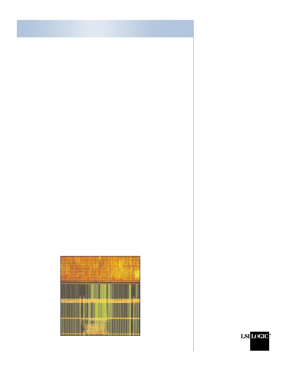
LSI401Z Digital Signal Processor
LSI401Z available in 0.25
mm technology.
Benefits
∑
400 MMAC sustained DSP performance
∑
Flexibility to optimize power consumption
∑
Reduced system memory cost
∑
High data throughput without processor
overhead
∑
High data bandwidth to off-chip devices
∑
RTOS support and increased system
integration
∑
High-speed link to I/O data streams
∑
Simple interfacing to industry-standard
micros
∑
Flexibility for direct control of off-chip
devices
∑
Low overhead on chip debug
∑
Very high processing density per unit
area

LSI Logic logo design is a registered trademark and ZSP is a
trademark of LSI Logic Corporation. All other brand and
product names may be trademarks of their respective
companies.
LSI Logic Corporation reserves the right to make changes to
any products and services herein at any time without notice.
LSI Logic does not assume any responsibility or liability
arising out of the application or use of any product or service
described herein, except as expressly agreed to in writing by
LSI Logic; nor does the purchase, lease, or use of a product or
service from LSI Logic convey a license under any patent
rights, copyrights, trademark rights, or any other of the
intellectual property rights of LSI Logic or of third parties.
Copyright ©1999 by LSI Logic Corporation.
All rights reserved.
For more information please call:
Europe +32.11.300.351
408.433.7700 Dept. JDS
www.lsilogic.com
LSI Logic Corporation
North American Headquarters
Milpitas, CA
Tel: 408.433.8000
Fax: 408.433.8989
LSI Logic Europe Ltd
European Headquarters
Bracknell, United Kingdom
Tel: 44.1344.426544
Fax: 44.1344.481039
LSI Logic KK Headquarters
Tokyo, Japan
Tel: 81.3.5463.7821
Fax: 81.3.5463.7820
Order No. R20013
999.1K.CM.TP ≠ Printed in USA
ISO 9000 Certified
Timers
The LSI401Z has two identical 16-bit on-board timers for real-time interrupt
generation. Each timer is fully programmable, and has a 6-bit pre-scaler and
interrupt capability. The timers can automatically reload with the initial count
so that periodic interrupts can be generated.
Synchronous Serial Ports
The device provides two identical synchronous serial ports that support 8- or
16-bit active or passive transfers. Transfers can be either burst or continuous,
depending on whether data transfer is intermittent or in a continuous bit stream.
The maximum transfer rate in active mode is 100 Mbps given a 200 MHz processor
clock frequency. In passive mode, the maximum transfer rate is 200 Mbps.
Host Processor Interface (HPI)
The Host Processor Interface, or HPI, is an asynchronous 16-bit parallel port
that is compatible with both Motorola and Intel style interfaces, and supports
word (16-bit) transfers. The maximum transfer rate for the HPI is half of the
processor clock frequency (100M words per second given a processor operating
frequency of 200 MHz).
Development Tools
The ZSP Processor family is fully supported by a GNU-based compiler, linker and
assembler, available for Windows 95/98/NT and Solaris 2 platforms. The ZSP
Architecture enables the C compiler to produce code unrivaled in code density
and execution speed by any DSP in its class, offering fast time to market with
optimal performance and cost. An integrated debug environment is available for
PC platforms.
An LSI401Z development platform is available, offering the following features:
∑
FLASH EPROM
∑
RS232C and JTAG-based host communication and code download
∑
128K words asynchronous program/data memory
∑
Dual audio codecs
LSI401Z Digital Signal Processor