 | –≠–ª–µ–∫—Ç—Ä–æ–Ω–Ω—ã–π –∫–æ–º–ø–æ–Ω–µ–Ω—Ç: LSI403LP | –°–∫–∞—á–∞—Ç—å:  PDF PDF  ZIP ZIP |
Document Outline
- LSI403LP Digital Signal Processor
- Figure�1 LSI403LP Block Diagram
- Features and Benefits
- Functional Description
- Instruction Set Summary
- Signal Descriptions
- Functional Waveforms
- Serial Port Timing
- External Memory Interface Unit (MXU) Timing
- Host Port Interface (HPI) Timing
- Figure�9 HPI Host Read, Intel Mode, two 16-bit reads, two items in FIFO (lof=1)
- Table�15 HPI Host Read, Intel Mode, two 16-bit reads, two items in FIFO (lof=1)
- Table�16 HPI Host Read, Intel Mode, two 8-bit reads, two items in FIFO
- Table�17 HPI Host Write, Intel Mode, two 16-bit writes, two spaces in FIFO (lof=1)
- Table�18 HPI Host Write, Intel Mode, two 8-bit writes, two spaces in FIFO
- Table�19 HPI Host Read, Motorola Mode, two 16-bit reads, 2 items in FIFO (lof=1)
- Table�20 HPI Host Read, Motorola Mode, two 8-bit reads, 2 items in FIFO (lof=1)
- Table�21 HPI Host Write, Motorola Mode, two 16-bit writes, 2 items in FIFO (lof=1)
- Table�22 HPI Host Write, Motorola Mode, two 8-bit writes, 2 items in FIFO (lof=1)
- Specifications

November 2002
1 of 42
Copyright © 2000≠2002 by LSI Logic Corporation. All rights reserved.
Preliminary ≠ Content Subject to Change
LSI403LP Digital
Signal Processor
Preliminary Datasheet
The LSI403LP is a 16-bit, fixed-point digital signal processor (DSP)
based on the ZSP
Æ
400 DSP core. The LSI403LP contains an entire DSP
system on a single chip, and is designed for applications requiring lower
power consumption, high throughput and flexibility such as consumer
and customer premises communications equipment.
The LSI403LP operates at a clock rate of 150 MHz for a maximum
effective throughput of 600 RISC-like MIPS. The LSI403LP RISC
architecture is easy to program, and it uses a four-way superscalar
pipeline with five stages to process up to 20 instructions at a time. The
processor's execution unit contains two multiplier/accumulator (MAC)
units and two arithmetic logic units (ALUs). The LSI403LP also supports
single cycle add-compare-select, bit manipulation, and 32-bit arithmetic
and logic operations.
The LSI403LP provides 16 Kwords of on-chip instruction Random-
Access Memory (RAM) and 16 Kwords of on-chip data RAM plus an
additional bank of 16 Kwords of RAM that can be configured for use as
instruction or data memory with an 8 Kword granularity. For optimum
I/O performance and flexibility, the LSI403LP contains two high-speed
time-division multiplexing (TDM) serial ports, a single 8-bit
host processor interface (HPI), an external memory interface unit (MXU),
and a 4-pin programmable I/O (PIO) port. This peripheral set is
supported by an 8-channel DMA controller, which can transfer data
between any peripheral and the on-chip memories. An IEEE 1149.1 Joint
Test Activity Group (JTAG) port supports program download and debug
in addition to boundary scan.
LSI Logic provides a software development kit containing an assembler,
linker, GUI debugger, simulator, C compiler, and JTAG-based hardware
emulator. Development tools are also available from Green Hills
Software, Inc.
The LSI403LP core logic operates at 1.2 V and its I/O operates at 3.3V,
and is packaged in a 208-pin plastic quad flat pack (PQFP) package.
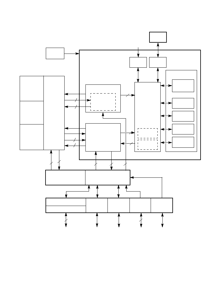
Figure 1
shows a block diagram of the LSI403LP.
Preliminary ≠ Content Subject to Change
2 of 42
LSI403LP Digital Signal Processor
Copyright © 2000≠2002 by LSI Logic Corporation. All rights reserved.
Figure 1
LSI403LP Block Diagram
Serial
Port 1
Serial
Port 0
JTAG
DEU
HPI
Execution Unit
rdA
wrA
DO
DI
64
64
Interrupts
ICU
PLL
DMA Controller
Instruction Unit
Instruction
Cache
Data
Memory
Data Unit
Pipeline
Control
Unit
Register
File
ALU
ALU
MAC
MAC
8
HPI = Host Processor Interface
ICU = Interrupt Control Unit
MXU
32
16
16
PIO(4)
64
32
A
DO
Program
Memory
DEU = Device Emulation Unit
Timer0
Timer1
DI
32
Load/Store Buffer
XBus
16/32
16
16
PLL = Phase-Locked Loop
XBus = External Bus
Configurable
Memory
Internal
Memory
Controller
16Kx16
16Kx16
16Kx16
64
32
Note:

Preliminary ≠ Content Subject to Change
LSI403LP Digital Signal Processor
3 of 42
Copyright © 2000≠2002 by LSI Logic Corporation. All rights reserved.
Features and Benefits
Processor
∑
RISC architecture
≠
Instruction grouping by hardware
for parallel execution
∑
Four-way superscalar architecture
≠
Two MACs
≠
Two ALUs
∑
600 RISC-like MIPS maximum
throughput at a clock rate of 150 MHz
∑
Multitasking support
≠
Low-latency interrupt structure with
programmable priority levels
≠
Efficient context switch support
∑
On-chip PLL for clock generation
Applications
∑
Optimized for communications
infrastructure applications
≠
Single-cycle, dual 16-bit MAC with
40-bit result
≠
Single-cycle, high-precision (32-bit)
MAC with 40-bit result
≠
Two-cycle complex multiply
≠
Control code optimized instructions
≠
Supported by wide range of VoIP
software
Technology
∑
208-pin PQFP package
Memory
∑
16 Kword internal instruction RAM
∑
16 Kword internal data RAM
∑
16 Kword configurable RAM
∑
1 Kword Boot RAM
∑
8-channel DMA controller with
continuous mode
≠
Supports fast I/O transfers
≠
High speed transfer from peripherals
to/from internal RAMs
∑
32-bit MXU
≠
Glueless interface to
synchronous-burst SRAMs
(SBSRAMs)
≠
18-bit address space (512 Kwords)
for instruction and data memory
∑
Glueless interface to 16-bit SRAMs
I/O
∑
Two high-speed TDM serial ports
≠
H.100/H.110 bitstream-compatible
≠
Integral u-Law / A-Law companding
∑
8-bit HPI
∑
4-pin PIO port
∑
IEEE 1149.1-compliant JTAG port
Timers
∑
Two 16-bit timers with a 6-bit prescaler
∑
Single-shot and continuous mode

Preliminary ≠ Content Subject to Change
4 of 42
LSI403LP Digital Signal Processor
Copyright © 2000≠2002 by LSI Logic Corporation. All rights reserved.
Functional Description
The LSI403LP contains an entire DSP system and allows the attachment
of external memory and peripherals. See
Figure 1
for a block diagram of
the LSI403LP.
Core Modules
The pipeline control unit groups instructions, resolves dependencies, and
schedules instructions for execution by the execution unit. The pipeline
control unit also processes interrupt requests forwarded from the ICU.
The LSI403LP contains a four-way, superscalar, five-stage pipeline. At
any time, up to 20 instructions may be in various stages of the pipeline.
The five pipeline stages of this machine are: Fetch/Decode (F/D), Group
(G), Read (R), Execute (E), and Write (W).
The pipeline control unit also contains two 16-bit timers for interrupt
generation. Both timers are fully-programmable and have 6-bit
prescalers. When enabled, the timers count down from the user-specified
initial value to zero at a rate determined by the scaled output of the
LSI403LP output clock. The timers generate an interrupt when zero is
reached. The timers can be configured to reload automatically with the
initial count to generate periodic interrupts.
The data unit fetches and stores data into the data cache. The data unit
contains the data prefetcher and cache, and contains the logic for two
circular buffers.
The instruction unit fetches instructions, decodes and dispatches them,
and places the instructions in the instruction cache. The instruction unit
contains the instruction cache, the instruction prefetcher, and the
instruction dispatch unit. The instruction unit also contains branch
prediction logic.
The control register file contains a set of 16-bit control registers used for
mode control, status, and flag information.
The execution unit performs all arithmetic and logical operations in the
LSI403LP. The execution unit contains two 16-bit ALUs, two
16-bit x 16-bit MAC units, and a general purpose (operand) register file.

Preliminary ≠ Content Subject to Change
LSI403LP Digital Signal Processor
5 of 42
Copyright © 2000≠2002 by LSI Logic Corporation. All rights reserved.
The two ALUs are identical and can be combined as a single 32-bit ALU.
The MAC units can perform two 16-bit x 16-bit multiply operations and a
single 40-bit accumulation per cycle, or one 32-bit x 32-bit multiply
operation and a single 40-bit accumulation per cycle.
Memory
The LSI403LP has three main sections of on-chip memory - internal
instruction RAM, internal data RAM and configurable RAM. The
configurable RAM is constructed from two 8 Kword blocks. Each of these
blocks can be configured as instruction or data memory via a control
register. The configurable RAM is disabled by default.
In addition to the other RAM, the LSI403LP contains a 1 Kword block of
instruction memory at 0xF800. This memory is available for use when
booting through the HPI port or for other purposes such as ISR space.
The memory interface unit connects the LSI403LP to off-chip memory or
peripherals through a 32-bit data bus and an 18-bit address bus. The
memory interface unit provides a glueless interface to 16-bit
asynchronous memory devices (ROM, EPROM, and SRAM) and 32-bit
SBSRAMs.
I/O Units
The LSI403LP contains two identical serial ports capable of 8- or 16-bit
active or passive transfers. In active mode, the serial port generates its
own bit clock and sync signals. The serial port bit clock frequency is
determined by the processor clock rate divided by a user-specified value.
The maximum transfer rate in both modes is one-half the processor clock
rate.
Both LSI403LP serial ports provide a TDM mode compatible with T1/E1
framers or the local serial bus of H.100/H.110 interface devices. The
TDM mode can also establish a serial multiprocessor communication link
with only three signals. The user selects the word length (8 or 16 bits)
and frame length (1≠128 time slots) for TDM transfers. Transmit and
receive time slots are programmed individually, and can be modified on
the fly.
Both serial ports can automatically transform 16-bit linear PCM data into
8-bit u-Law or A-Law companded data before transmission and/or