B E N E F I T S
∑ Provides complete end-to-end
protection of the SCSI I/O with
Cyclic Redundancy Check
(CRC) and Asynchronous
Information Protection (AIP)
∑ Provides robust performance
with SureLINK
TM
domain validation
∑ Migrates easily from Ultra2 SCSI
∑ Supports all major
operating systems
∑ Protects SCSI investments
∑ Paves the way to Ultra320 SCSI
P C I - D U A L C H A N N E L U L T R A 1 6 0 S C S I
C O N T R O L L E R O V E R V I E W
The LSI53C1010 is a highly integrated PCI-Dual Channel Ultra160 SCSI
Controller. The LSI53C1010 is 100 percent compatible with the Ultra160
SCSI initiative and provides additional features that ensure robust Ultra160
system operation. The LSI53C1010 provides a seamless migration path
from the LSI53C896 PCI-Dual Channel Ultra2 SCSI Controller with
pin compatibility.
A P P L I C A T I O N S
∑ Servers ≠ Internet/Intranet network, video, e-mail, printing, database
management, and financial applications
∑ Workstations ≠ CAD/CAM, industrial simulation, etc.
∑ Host attach for RAID and JBOD mass storage subsystems ≠ Anywhere data
access is the bottleneck
LSI53C1010
ULTRA160 SCSI CONTROLLER
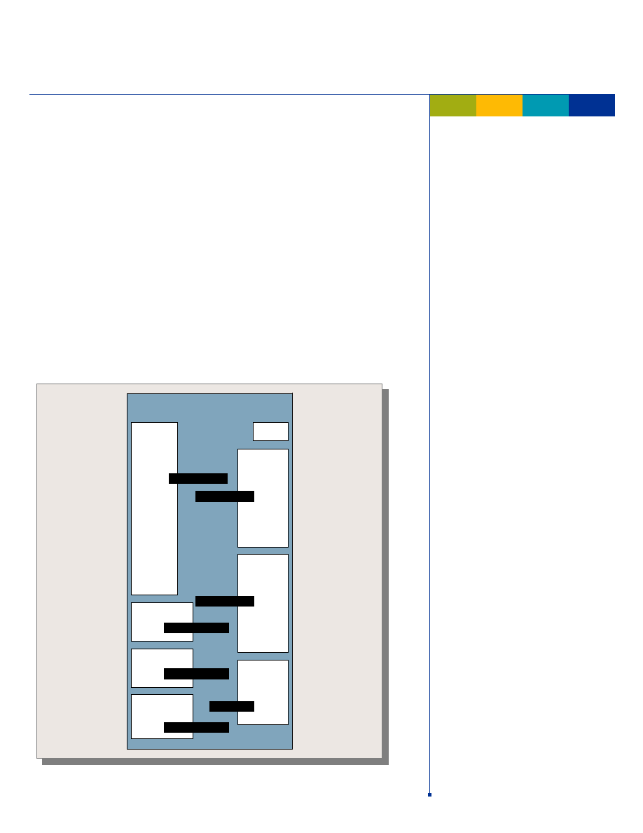
Figure 1. SCSI on the motherboard
Host PCI
Bridge
64-bit, 33/66 MHz Primary PCI Bus
Flash
(Up to 1 MB)
NVRAM
(2)
LSI53C1010
PCI-Ultra160 SCSI
SCSI
SCSI
Ultra160 SCSI Bus

K E Y F E A T U R E S
∑ Pin compatible with
LSI53C896 controller
∑ Design board to accommodate
either device in the same socket
∑ Op code (software) compatible
∑ No external memory required
∑ 64-bit, 33/66 MHz PCI interface
∑ Theoretical 528 MBps (on
66 MHz part) zero wait state
transfer rate
∑ 64-bit addressing supported
through Dual Address Cycle
(DAC)
∑ Compliant with PCI 2.2, PCI
Power Management 1.1
and PC99
∑ Supports Ultra160 SCSI
∑ Double transition clocking for
160 MBps throughput on
each channel
∑ CRC
∑ Domain validation
∑ AIP
∑ Covers all non-data, including
command, status and messages
∑ High-performance PCI
multifunction device
∑ Presents one electrical load
to PCI bus
∑ Two independent wide Ultra160
SCSI channels
∑ SCSI Interrupt Steering Logic
(SISL) alternate interrupt routing
for RAID applications
U L T R A 1 6 0 S C S I F E A T U R E S
Double transition clocking enables throughput of up to 160 MBps on each
channel for a total of 320 MBps, without increasing the interface clock rate.
Cyclic Redundancy Check (CRC) improves the reliability of SCSI data transmission
through enhanced detection of communication errors. CRC provides extra
data protection for marginal cable plants and external devices. CRC is the
best way to ensure data protection during hot plugging. It uses the same
proven CRC algorithm used by FDDI, Ethernet, and Fibre Channel, and
detects all single bit errors, all double bit errors, all odd number of errors,
and all burst errors up to 32 bits long. To provide complete end-to-end
protection of the SCSI I/O, AIP protects all non-data phases, augmenting the
CRC feature of Ultra160.
SureLINK domain validation technology detects the configuration of the SCSI
bus and automatically tests and adjusts the SCSI transfer rate to optimize
interoperability. The LSI53C1010 exceeds Ultra160 by providing not only
Basic (Level 1) and Enhanced (Level 2) domain validation, but adds Margined
(Level 3) domain validation. This enhancement margins LVD drive strength
and clock signal timing characteristics to identify marginal Ultra160 systems.
H A R D W A R E / S O F T W A R E O V E R V I E W
P C I I n t e r f a c e
The host PCI interface complies with PCI Local Bus Specification Revision
2.2, and implements a 64-bit/66 MHz PCI bus. It is backward compatible
with 32-bit/33 MHz buses. Additionally, support for DAC is provided.
The LSI53C1010 is a true PCI multifunction device in that it presents one
electrical load to the PCI bus. It uses one REQ/-GNT/pair to arbitrate for
PCI bus mastership, and separate interrupt signals are generated for SCSI
Function A and SCSI Function B for maximum performance.
The LSI53C1010 complies with PCI Power Management Interface
Specification Revision 1.1 and PC 99, supporting power states D0, D1, D2,
D3hot and D3cold, power management capabilities registers, and program-
mable values for PCI Subsystem Vendor ID and Subsystem ID. Extended
access cycles (Memory Read Line, Memory Read Multiple, and Memory
Write and Invalidate) are also supported.
LSI53C1010 Ultra160 SCSI Controller
2
K E Y F E A T U R E S ( C o n t i n u e d )
∑ Proven integrated LVDlink
transceivers for direct attach to
either Low Voltage Differential
(LVD) or single-ended (SE)
SCSI buses
∑ Comprehensive SureLINK
domain validation
∑ Basic (Level 1) with
inquiry command
∑ Enhanced (Level 2) with
read/write buffer
∑ Margined (Level 3) with
margining of LVD drive
strength and programmable
skew test
∑ IEEE 1149.1 JTAG boundary scan
∑ Flash and local memory interface
∑ Packaged in a 329 PBGA
∑ Supported in Storage Device
Management System (SDMS
TM
)
software release 4.6
∑ Full operating system support:
- Windows
Æ
NT
Æ
4.0,
95/98 and 2000
- Linux
TM
- Solaris
TM
- UnixWare
TM
- Novell
Æ
NetWare
Æ
- OS/2
∑ Server Management Cl
(component instrumentation)
S C S I P r o c e s s o r s
The LSI53C1010 provides two independent Ultra160 SCSI controllers on
a single chip. Each controller supports wide Ultra160 SCSI synchronous transfer
rates up to 160 MBps on a LVD SCSI bus. Integrated LVDlink
TM
transceivers
support both LVD and single-ended signals with no external transceivers
required. Fast SCSI, Ultra SCSI, Ultra2 SCSI, and Ultra160 SCSI are all
supported by the LSI53C1010.
An on-chip SCSI clock quadrupler allows the chip to achieve Ultra160 SCSI
transfer rates with an input frequency of 40 MHz. The 8 KB of internal RAM per
channel for SCRIPTS
TM
instruction storage allow all accesses to remain internal,
reducing the time spent on the PCI bus. A 944-byte DMA FIFO on each channel
allows the device to efficiently burst up to 512 bytes across the PCI bus. SCSI
bus phase mismatches are handled in SCRIPTS, reducing CPU utilization.
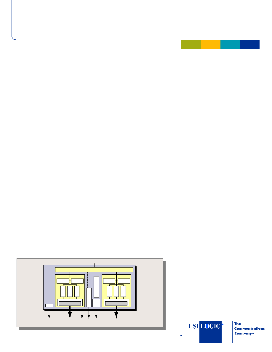
Figure 2. LSI53C1010 functional signal grouping
CLK
RST/
REQ/
GNT/
REQ64/
ACK64/
AD[63:0]
C_BE[7:0]/
IDSEL
FRAME/
IRDY/
TRDY/
DEVSEL/
STOP/
PERR/
SERR/
PAR
PAR64
INTA/
INTB/
ALT_INTA/
ALT_INTB/
INT_DIR
M66EN
ENABLE66
SCLK
RBIAS
A_SD[15:0]/
A_SDP[1:0]/
A_DIFFSENS
A_GPIO0_FETCH/
A_GPIO1_MASTER/
A_GPIO2
A_GPIO3
A_GPIO4
B_GPIO0_FETCH/
B_GPIO1_MASTER/
B_GPIO2
B_GPIO3
B_GPIO4
MWE/
MCE/
MOE/_TESTOUT
MAS0/
MAS1/
MAD7-0
329 PBGA
LSI53C1010
64-bit, 66 MHz PCI
SCSI Function A
A_SC_D/
A_SI_O/
A_SMSG/
A_SREQ/
A_SREQ2/
A_SACK/
A_SACK2/
A_SBSY/
A_SATN/
A_SRST/
A_SSEL/
B_SD[15:0]/
B_SDP[1:0]/
B_DIFFSENS
B_SC_D/
B_SI_O/
B_SMSG/
B_SREQ/
B_SREQ2/
B_SACK/
B_SACK2/
B_SBSY/
B_SATN/
B_SRST/
B_SSEL/
TEST_RSTN
TEST_HSC
MOE/_TESTOUT
TCK
TMS
TDI
TDO
TEST_PD
SCAN_MODE
SCSI Function B
Test Interface
SCSI Function A GPIO
SCSI Function B GPIO
Memory Interface
3
M E M O R Y I N T E R F A C E S
The LSI53C1010 supports up to 1 MB of external expansion ROM
through a parallel interface, for add-in card designs. For ease of software
development and field upgrades of the ROM, the interface supports local
programming of FLASH memory. A serial 2-wire interface on each SCSI
channel provides a connection to an external serial EEPROM for storing
Subsystem Vendor ID and Subsystem ID.
S O F T W A R E
The LSI53C1010 is supported with the proven SDMS software. SDMS software
enables the performance enhancements of Ultra160 data transfer speed increases
and improved PCI bus utilization capabilities included in the LSI53C1010.
The LSI53C1010 reliability capabilities of AIP and CRC are enabled and
managed by the SDMS software. SDMS software implements the manageability
improvements of the LSI Logic SureLINK domain validation technology. SureLINK
technology extends standard domain validation with the addition of full cable
plant margining. The cable plant margining capability, exclusive to LSI Logic's
Ultra160 solution, includes end-to-end margining from the LSI53C1010 through
LSI Logic's LSI53C180 SCSI bus expander to the target device. The domain
validation capability of SDMS software is available as an independent application
as well as integrated in the DMI 2.0 based system management solution for
enterprise class implementations. SDMS software includes BIOS and OSV
certified drivers for all major operating systems including DOS with ASPI
support, Windows 95/98, Windows NT/2000, UnixWare, OS/2, NetWare,
Solaris and Linux. A complete set of SCSI utilities rounds out the software
solution, which includes a DMI 2.0 based system management software for
Windows NT, NetWare, UnixWare, Solaris and Linux, and a stand-alone or
snap-in DMI browser applet and SureLINK applet.
For more information please visit
the
LSI Logic web site at:
http://storageio.lsilogic.com
LSI Logic Corporation
North American Headquarters
Milpitas, CA
Tel: 866 574 5741
LSI Logic Europe Ltd.
European Headquarters
United Kingdom
Tel: 44 1344 426544
Fax: 44 1344 481039
LSI Logic KK Headquarters
Tokyo, Japan
Tel: 81 3 5463 7165
Fax 81 3 5463 7820
ISO 9000 Certified
LSI Logic logo design and TolerANT are registered
trademarks, and LVDlink, SCRIPTS, SDMS, and
SureLINK are trademarks of LSI Logic Corporation.
All other brand and product names may be trade-
marks of their respective companies.
LSI Logic Corporation reserves the right to make
changes to any products and services herein at
any time without notice. LSI Logic does not
assume any responsibility or liability arising out of
the application or use of any product or service
described herein, except as expressly agreed to
in writing by LSI Logic; nor does the purchase,
lease, or use of a product or service from LSI
Logic convey a license under any patent rights,
copyrights, trademark rights, or any other of the
intellectual property rights of LSI Logic or of third
parties.
Copyright ©2001 by LSI Logic Corporation.
All rights reserved.
Order No. S20010
7/01-1M ≠ Printed in USA
LSI53C1010 Ultra160 SCSI Controller
Ultra160 SCSI
Controller Block
Host PCI Bus (64-bit, 33/66 MHz)
PCI Master and Slave Control Block, PCI Configuration Registers (2 sets), and SCSI Arbitration
8 Dword SCRIPTS
Prefetch Buffer
8 KB SCRIPTS
RAM
944-b
yte
DMA FIFO
SCSI SCRIPTS
Processor
Opening
registers
SCSI FIFO and SCSI Control Block
TolerANT
Æ
and LVDlink
Ultra160 SCSI
Controller Block
8 Dword SCRIPTS
Prefetch Buffer
8 KB SCRIPTS
RAM
944-b
yte
DMA FIFO
SCSI SCRIPTS
Processor
Opening
registers
SCSI FIFO and SCSI Control Block
TolerANT
Æ
and LVDlink
JTAG
Ser
ial EEPR
OM Controller
and A
uto-Configur
ation
R
O
M/Flash Memor
y
Control
Local
Memory
Bus
JTAG
Wide Ultra160 SCSI Bus
(A Channel)
2-wire Serial
EEPROM Bus
(one per channel)
ROM/Flash
Memory Bus
Wide Ultra160 SCSI Bus
(B Channel)
Figure 3. LSI53C1010 functional block diagram
4