The
Communications
Company
TM
O V E R V I E W
Asymmetric digital subscriber line (ADSL) technology provides a viable
solution to meet the emerging need for high-bandwidth communications to
the home while utilizing existing twisted-pair copper infrastructure. To simplify
the design and reduce deployment costs, LSI Logic has developed DPS8003, an
analog front-end (AFE) that is designed to perform all of the analog functions of
the receive (RX) and transmit (TX) paths for ADSL for G.lite, excluding POTS
reject filtering and high-voltage line drivers/receivers. The DPS8003 requires no
external circuitry beyond a pair of precision resistors and bypass/coupling
capacitors. Note that (a) for full compliance with the ITU G.992.2 transmit PSD
masks, additional off-chip filtering in the TX path is needed; (b) in frequency
division multiplexing (FDM) systems, additional off-chip bandsplit filtering may
be required for system optimization.
The linearity and noise performance of the analog signal paths enable the
chip to successfully transmit and receive data at 1.5 Mbits/s on the longest lines
-- above 18 kfeet of AWG24 wire. The chip can be utilized in systems
employing either echo cancellation (EC) or FDM, and is also fully compatible
with the splitterless G.lite standard.
SpeedREACH
TM
DPS8003 -- G.lite
ADSL Analog Front End for CPE
F E A T U R E S
∑ ADSL AFE for CPE with full receive (RX)
and transmit (TX) analog signal path
for G.lite (excluding POTS reject filter
and high-voltage line drivers/receivers)
∑ Fully monolithic: 2 precision resistors,
2 non-critical resistors, and decoupling
capacitors required
∑ Support for both echo-cancelled and
FDM-based systems; full analog path
support in hardware
∑ Compatible with ITU G.992.2 (G.lite)
standard
∑ 14-bit linear ADCs and dual 14-bit
linear DACs
∑ 4th-order lowpass filters for RX/TX paths,
with ±5% cutoff frequency accuracy
∑ RX channel: support for both 138 kHz
and 276 kHz (for ADSL over ISDN)
∑ TX channel: support for 552 kHz (G.lite)
∑ RX path PGAs: 44 dB in 0.25 dB steps
∑ TX path PAAs: 24 dB in 1 dB steps
∑ Entire RX channel linearity: 80 dB MTPR
∑ Entire TX channel linearity: 80 dB MTPR
∑ 12-bit DAC to support external VCXO
∑ RX input-referred noise at peak gain:
160 dBm/Hz at 300 kHz
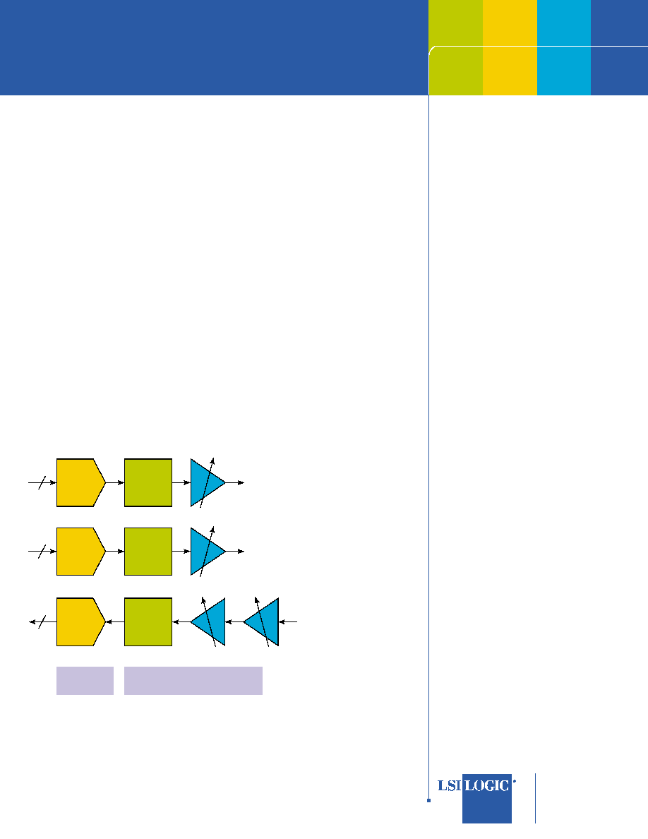
DAC
4.4MHz
Echo Out
16
ADC
2.2MS/s
RX
Filter
552kHz
RX In
Fine PGA
PAA
16
Low-Noise Coarse PGA
TX LPF
138kHz/
276kHz
DAC
4.4MHz
TX Out
16
PAA
TX LPF
138kHz/
276kHz
Support Blocks
VCXO DAC
PGA -- Programmable Gain Amp
PAA -- Programmable Attenuator Amp
Figure 1. Block diagram of the SpeedREACH DPS8003 AFE.

The
Communications
Company
TM
SpeedREACH
TM
DPS8003
The RX portion of the chip comprises a low-noise front end programmable
gain amplifier (PGA), an anti-aliasing filter, and a 16-bit analog-to-digital
converter (ADC). The TX portion consists of two independent signal paths, one
for the primary TX signal and one to support echo. One key feature is excellent
matching between the echo path and the primary TX path, minimizing difficulties
in echo cancellation arising from mismatch between the two. Each path consists
of a 16-bit digital-to-analog converter (DAC), a transmit lowpass filter, and a
programmable attenuation amplifier (PAA). To simplify the overall system design,
DAC droop compensation is handled internally, removing this burden from the
back-end signal processing.
Apart from the primary signal paths, the chip also contains support circuitry
for other functions required in an ADSL modem. To assist in timing recovery, a
12-bit DAC is present to drive an off-chip voltage controlled crystal oscillator.
The chip's digital input/output interfaces are designed to be as simple as possible,
emphasizing ease of design-in and evaluation. The primary digital ADC/DAC
interfaces are on separate 16-bit wide busses: 16 for the ADC, and 16 for the
primary TX path DAC. When the echo path is used, the chip accepts digital data
at a 2X rate and alternate digital words are passed in a ping-pong fashion to the
main TX path and the echo path.
A 4-wire serial port provides a simple DSP interface. The serial port is used
to modify internal register values, which in turn control attenuation/gain settings,
filter bandwidths and the power down of individual blocks. The chip is powered
off a +5 V supply, while all digital I/Os run off a +3.3 V supply. The DPS8003 is
available in a 128-pin MQFP plastic package. The operating temperature
range is between 0∞ C and +70∞ C.
D I F F E R E N C E S F R O M S P E E D R E A C H D P S 8 0 0 1
This device is similar to the DPS8001. The differences are as follows:
∑ The temperature range is from 0 to +70∞C.
∑ The RX path performance (PGA, filter, ADC) is only guaranteed for a G.lite
configuration--i.e., for downstream band up to 552 kHz, and ADC running
at 2.208 MS/s
For more information please call:
LSI Logic Corporation
North American Headquarters
Milpitas, CA
Tel: 800 574 4286
LSI Logic Europe Ltd.
European Headquarters
United Kingdom
Tel: 44 1344 426544
Fax: 44 1344 481039
LSI Logic KK Headquarters
Tokyo, Japan
Tel: 81 3 5463 7165
Fax: 81 3 5463 7820
LSI Logic web site
www.lsilogic.com
LSI Logic logo design, is a registered trademark
and SpeedREACH is a trademark of LSI Logic
Corporation. All other brand and product names
may be trademarks of their respective companies.
LSI Logic Corporation reserves the right to make
changes to any products and services herein at any
time without notice. LSI Logic does not assume any
responsibility or liability arising out of the
application or use of any product or service
described herein, except as expressly agreed to in
writing by LSI Logic; nor does the purchase, lease,
or use of a product or service from LSI Logic
convey a license under any patent rights,
copyrights, trademark rights, or any other of the
intellectual property rights of LSI Logic or of third
parties.
Copyright ©2001 by LSI Logic Corporation.
All rights reserved.
Order No. R20031
101.1k.JG.LT - Printed in USA