V 2.00
GaAs SPDT Switch
DC - 8 GHz
M A S W 8 0 0 0
Guaranteed Specifications* * @ + 2 5
∞
C***
Frequency Range
DC-8.0 GHz
Insertion Loss
DC-2.0 GHz
0.8 dB Max
DC-4.0 GHz
0.9 dB Max
DC-8.0 GHz
1.0 dB Max
VSWR
DC-2.0 GHz
1.3:1 Max
DC-4.0 GHz
1.4:1 Max
DC-8.0 GHz
1.5:1 Max
Isolation
DC-2.0 GHz
37 dB Min
DC-4.0 GHz
30 dB Min
DC-8.0 GHz
20 dB Min
Operating Characteristics
Impedance
50
Nominal
Switching Characteristics
Trise, Tfall (10/90% or 90/10% RF)
2 ns Typ
Ton, Toff (50% CTL to 90/10% RF)
4 ns Typ
Transients (in-Band)
20 mV Typ
Input Power for 1 dB Compression
Control Voltages (Vdc)
0/-5
0/-8
0.05 GHz
+20 dBm
+22 dBm Typ
0.5-8 GHz
+27 dBm
+30 dBm Typ
Intermodulation Intercept point
(for two-tone input power up to +5 dBm)
Intercept Points
IP2
IP3
0.05 GHz
+53 dBm
+40 dBm Typ
0.5-8 GHz
+78 dBm
+52 dBm Typ
Control Voltages (Complimentary Logic)
Vin Low
0 to -0.2V @ 20 µA Max
Vin Hi
-5V @ 50 µA Typ to -8V @ 350 µA Max
Die Size
0.046" x 0.036" X 0.010"
(1.15mm X 0.90mm X 0.25mm)
** All specifications apply with 50
impedance connected to all RF ports,
0 and -5 Vdc control voltages.
*** Loss change 0.0025 dB/∞C . (From -55∞C to +85∞C)
Features
q
Low Insertion Loss, 0.8 dB Typical @ 8 GHz
q
Fast Switching Speed, 3 ns Typical
q
Flexible Bonding Configurations
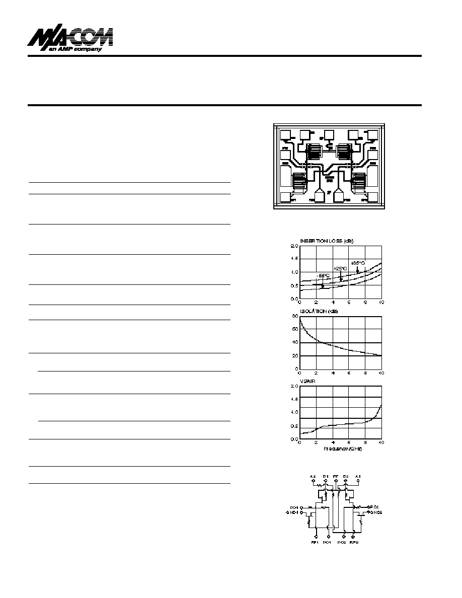
Typical Performance
Schematic

V 2.00
Handling Precautions
Pe rmanent damage to the MASW8000 may occur if the fo l-
l owing precautions are not adhered to:
A . Cleanliness -- The MASW8000 should be handled in a
clean env i r o n m e n t . DO NOT attempt to clean unit after
the MASW8000 is installed.
B. Static Sensitivity -- All chip handling equipment and per-
sonnel should be DC gr o u n d e d .
C. Transient -- Avoid instrument and power supply tra n s i e n t s
while bias is applied to the MASW8000. Use shielded
signal and bias cables to minimize inductive pick - u p.
D. Bias --Apply voltage to either of the complementary con-
trol port A1/B2 or A2/B1 only when the other is gr o u n d e d .
Neither port should be allowed to "float".
E .G e n e ral Handling -- It is recommended that the
MASW8000 chip be handled along the long side of the
die with a sharp pair of bent twe e ze r s. DO NOT touch the
s u r face of the chip with fingers or twe e ze r s.
Mounting
The MASW8000 is back - m e t a l l i zed with Pd/Ni/Au
(100/1,000/10,000≈) metallization. It can be die-mounted
with AuSn eutectic prefo rms or with thermally conductive
e p ox y. The package surface should be clean and flat befo r e
a t t a c h m e n t .
Eutectic Die Attach:
A . A 80/20 gold/tin prefo rm is recommended with a wo rk
s u r face temperature of approximately 255∞C and a tool
t e m p e rature of 265∞C. When hot 90/10 nitrogen/hy d r o g e n
gas is applied, tool tip temperature should be approx i-
mately 290∞C.
B. DO NOT expose the MASW8000 to a tempera t u r e
greater than 320∞C for more than 20 seconds. No more
than 30 seconds of scru bbing should be required fo r
a t t a c h m e n t .
E p oxy Die Attach:
A . Apply a minimum amount of epoxy and place the
MASW8000 into position. A thin epoxy fillet should be
v i s i ble around the perimeter of the chip.
B. Cure epoxy per manu fa c t u r e r 's recommended schedule.
C. E l e c t rically conductive epoxy may be used but is not
r e q u i r e d .
Wire Bonding
A . Ball or wedge bond with 1.0 mil diameter pure gold wire.
T h e rmosonic wirebonding with a nominal stage tempera-
ture of 150∞C and a ball bonding force of 40 to 50 gra m s
or wedge bonding force of 18 to 22 grams is recommend-
e d .U l t rasonic energy and time should be adjusted to the
m i n i mum levels to achieve reliable wirebonds.
B. Wirebonds should be started on the chip and term i n a t-
ed on the pack a g e. GND bonds should be as short as
p o s s i bl e ; at least three and no more than four bond
wires or two 3-mil ri bbons from ground pads to pack a g e
are recommended.
Maximum Ratings
A. Control Voltage (A1/B2 or A2/B1):≠8.5 Vdc
B. Max Input RF Power:
+34 dBm
C. Storage Temperature:
≠65∞C to +175∞C
D. Max Operating Temperature:
+175∞C
BondPad Dimensions
Inches (mm)
RF:
0.004 x 0.004
(0.100 x 0.100)
RF1, RF2:
0.004 x 0.004
(0.100 x 0.100)
A1, A2, B1, B2:
0.004 x 0.004
(0.100 x 0.100)
PC1, PC2
0.004 x 0.004
(0.100 x 0.100)
GND1, GND2:
0.005 x 0.009
(0.110 x 0.225)
Truth Ta bl e * * * *
Control Inputs
Condition Of Switch
A1/B2
A2/B1
RF1
RF2
V
IN
Hi
V
IN
Low
On
Off
V
IN
Low
V
IN
Hi
Off
On
****For normal SPDT operation A1 is connected to B2 and
A2 is connected to B1.
Die Size
Inches (mm)
0.046 x 0.036 x 0.010
(1.15 x 0.90 x 0.25)