 | –≠–ª–µ–∫—Ç—Ä–æ–Ω–Ω—ã–π –∫–æ–º–ø–æ–Ω–µ–Ω—Ç: MRF1004 | –°–∫–∞—á–∞—Ç—å:  PDF PDF  ZIP ZIP |
The RF Line
Microwave Pulse
Power Transistors
Designed for Class B and C common base amplifier applications in short and
long pulse TACAN, IFF, DME, and radar transmitters.
∑
Guaranteed Performance @ 1090 MHz, 35 Vdc
Output Power = 4.0 Watts Peak
Minimum Gain = 10 dB
∑
100% Tested for Load Mismatch at All Phase Angles with 10:1 VSWR
∑
Industry Standard Package
∑
Nitride Passivated
∑
Gold Metallized, Emitter Ballasted for Long Life and Resistance to
Metal Migration
∑
Internal Input Matching for Broadband Operation
MAXIMUM RATINGS
Rating
Symbol
Value
Unit
Collector≠Emitter Voltage
V
CEO
20
Vdc
Collector≠Base Voltage
V
CBO
50
Vdc
Emitter≠Base Voltage
V
EBO
3.5
Vdc
Collector Current -- Continuous
I
C
250
mAdc
Total Device Dissipation @ T
C
= 25
∞
C (1)
Derate above 25
∞
C
P
D
7.0
40
Watts
mW/
∞
C
Storage Temperature Range
T
stg
≠65 to +150
∞
C
THERMAL CHARACTERISTICS
Characteristic
Symbol
Max
Unit
Thermal Resistance, Junction to Case (2)
R
JC
25
∞
C/W
ELECTRICAL CHARACTERISTICS
(T
C
= 25
∞
C unless otherwise noted)
Characteristic
Symbol
Min
Typ
Max
Unit
OFF CHARACTERISTICS
Collector≠Emitter Breakdown Voltage
(I
C
= 5.0 mAdc, I
B
= 0)
V
(BR)CEO
20
--
--
Vdc
Collector≠Emitter Breakdown Voltage
(I
C
= 5.0 mAdc, V
BE
= 0)
V
(BR)CES
50
--
--
Vdc
Collector≠Base Breakdown Voltage
(I
C
= 5.0 mAdc, I
E
= 0)
V
(BR)CBO
50
--
--
Vdc
Emitter≠Base Breakdown Voltage
(I
E
= 1.0 mAdc, I
C
= 0)
V
(BR)EBO
3.5
--
--
Vdc
Collector Cutoff Current
(V
CB
= 35 Vdc, I
E
= 0)
I
CBO
--
--
0.5
mAdc
ON CHARACTERISTICS
DC Current Gain
(I
C
= 75 mAdc, V
CE
= 5.0 Vdc)
h
FE
10
--
100
--
NOTES:
(continued)
1. These devices are designed for RF operation. The total device dissipation rating applies only when the device is operated as RF amplifiers.
2. Thermal Resistance is determined under specified RF operating conditions by infrared measurement techniques.
MRF1004MB
4.0 W, 960≠1215 MHz
MICROWAVE POWER
TRANSISTORS
NPN SILICON
CASE 332A≠03, STYLE 1
Order this document
by MRF1004MB/D
SEMICONDUCTOR TECHNICAL DATA
1
REV 8
ELECTRICAL CHARACTERISTICS -- continued
(T
C
= 25
∞
C unless otherwise noted)
Characteristic
Symbol
Min
Typ
Max
Unit
DYNAMIC CHARACTERISTICS
Output Capacitance
(V
CB
= 35 Vdc, I
E
= 0, f = 1.0 MHz)
C
ob
--
3.3
5.0
pF
FUNCTIONAL TESTS
(Pulse Width = 10
µ
s, Duty Cycle = 1.0%)
Common≠Base Amplifier Power Gain
(V
CC
= 35 Vdc, P
out
= 4.0 W pk, f = 1090 MHz)
G
PB
10
11
--
dB
Collector Efficiency
(V
CC
= 35 Vdc, P
out
= 4.0 W pk, f = 1090 MHz)
40
45
--
dB
Load Mismatch
(V
CC
= 35 Vdc, P
out
= 4.0 W pk, f = 1090 MHz,
VSWR = 10:1 All Phase Angles)
No Degradation in Power Output
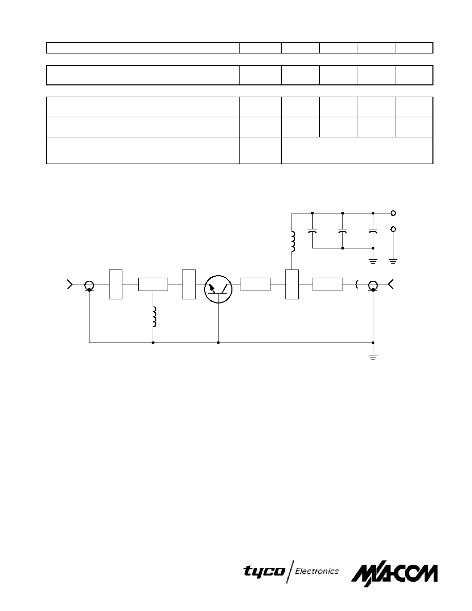
Figure 1. 1090 MHz Test Circuit
C1 -- 0.1
µ
F
C2, C4 -- 220 pF Chip Capacitor
C3 -- 20
µ
F, 50 V Electrolytic
L1, L2 -- 3 Turns #18 AWG, 1/8
ID
Z1≠Z6 Distributed Microstrip Elements, See Photomaster
Board Material -- 0.031
Thick Glass Teflon
RF
INPUT
RF
OUTPUT
C4
+
V
CC
= 35 Vdc
L1
D.U.T.
Z1
-
L2
Z2
Z3
Z4
Z5
Z6
C1
C2
C3
+
-
2
REV 8
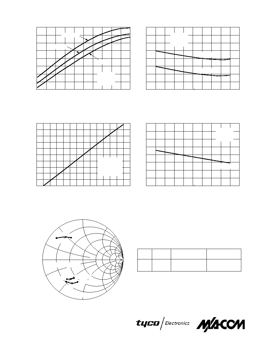
TYPICAL CHARACTERISTICS
Figure 2. Output Power versus Input Power
Figure 3. Output Power versus Frequency
Figure 4. Output Power versus Supply Voltage
Figure 5. Power Gain versus Frequency
Figure 6. Series Equivalent Input/Output Impedance
f
MHz
Z
in
Ohms
Z
OL
* (P
in
= 400 mW pk)
Ohms
960
1090
1215
5.0 + j17.5
10 + j23
16 + j29.5
23.5 ≠ j26
18.5 ≠ j25
15.5 ≠ j23.5
Z
OL
* = Conjugate of the optimum load impedance into which the device
Z
OL
* =
output operates at a given output power, voltage, and frequency.
Z
OL
* (P
out
= 4.0 W pk)
Ohms
22.5 ≠ j36
15 ≠ j32.5
11 ≠ j23
P
, OUTPUT
POWER (W pk)
out
150
P
in
, INPUT POWER (mW pk)
6.5
1.215 GHz
V
CC
= 35 V
t
P
= 10
µ
s
D = 1%
5.5
4.5
3.5
2.5
250
350
450
550
650
P
, OUTPUT
POWER (W pk)
out
960
8
f, FREQUENCY (MHz)
1090
1215
P
in
= 650 mW pk
400 mW pk
V
CC
= 35 V
t
P
= 10
µ
s
D = 1%
P
, OUTPUT
POWER (W pk)
out
V
CC
, SUPPLY VOLTAGE (V)
20
25
30
35
P
in
= 400 mW pk
t
P
= 10
µ
s
D = 1%
f = 1090 MHz
7
6
5
4
5
4
3
G
PB
, POWER GAIN (dB)
960
16
f, FREQUENCY (MHz)
1090
1215
14
12
10
8
P
out
= 4 W pk
V
CC
= 35 V
t
P
= 10
µ
s
D = 1%
+j50
+j100
+j150
+j250
+j500
-j500
-j250
-j150
-j100
-j50
-j25
-j10
0
+j10
+j25
Z
in
25
50
100 150
250 500
10
1090
1215
Z
OL
* (P
out
= 4 W pk)
1090
1215
1215
Z
OL
* (P
in
= 650 mW pk)
1090
COORDINATES IN OHMS
1.09 GHz
f = 0.96 GHz
f = 960 MHz
f = 960 MHz
f = 960 MHz
3
REV 8
TYPICAL CHARACTERISTICS
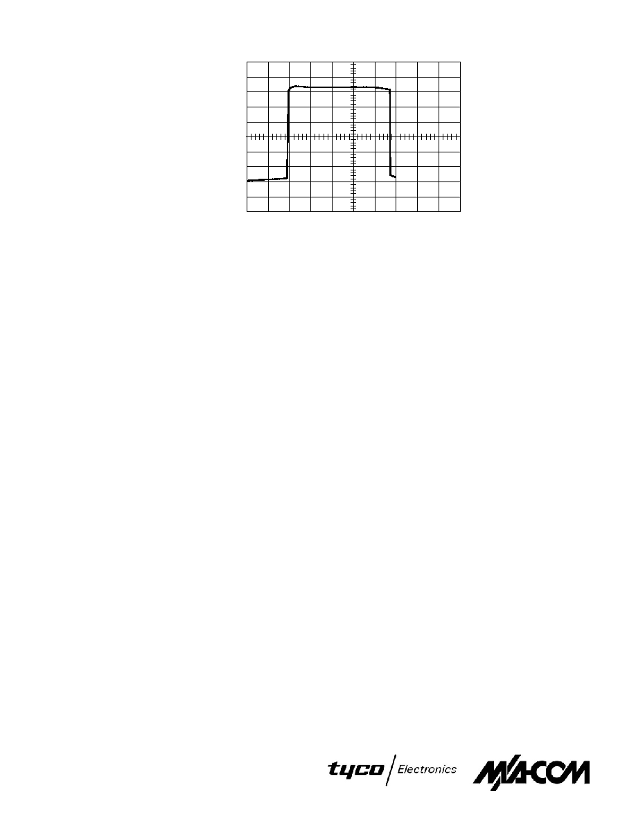
Figure 7. Typical Long Pulse Performance
P
out
= 4 W pk
V
CC
= 35 V
t
P
= 1 ms
D = 10%
f = 1090 MHz
4
REV 8
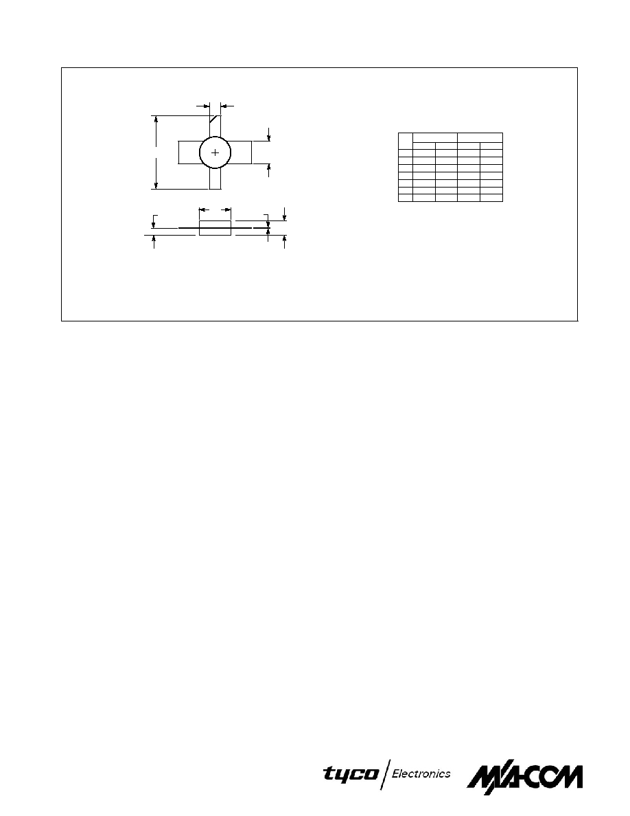
PACKAGE DIMENSIONS
CASE 332A≠03
ISSUE D
NOTES:
1. DIMENSIONING AND TOLERANCING PER ANSI
Y14.5M, 1982.
2. CONTROLLING DIMENSION: INCH.
STYLE 1:
PIN 1. BASE
2. EMITTER
3. BASE
4. COLLECTOR
K
F
D
SEATING
1
4
3
2
PLANE
H
A
J
C
DIM
MIN
MAX
MIN
MAX
MILLIMETERS
INCHES
A
0.270
0.290
6.86
7.36
C
0.115
0.135
2.93
3.42
D
0.195
0.205
4.96
5.20
F
0.095
0.105
2.42
2.66
H
0.050
0.070
1.27
1.77
J
0.003
0.007
0.08
0.17
K
0.600
---
15.24
---
5
Specifications subject to change without notice.
n
North America: Tel. (800) 366-2266, Fax (800) 618-8883
n
Asia/Pacific: Tel.+81-44-844-8296, Fax +81-44-844-8298
n
Europe: Tel. +44 (1344) 869 595, Fax+44 (1344) 300 020
Visit www.macom.com for additional data sheets and product information.
REV 8