The RF Line
NPN Silicon Push-Pull
RF Power Transistor
Designed primarily for wideband large≠signal output and driver amplifier
stages in the 30 to 500 MHz frequency range.
∑
Specified 28 Volt, 400 MHz Characteristics --
Output Power = 125 W
Typical Gain = 10 dB
Efficiency = 55% (Typ)
∑
Built≠In Input Impedance Matching Networks for Broadband Operation
∑
Push≠Pull Configuration Reduces Even Numbered Harmonics
∑
Gold Metallization System for High Reliability
∑
100% Tested for Load Mismatch
6
7
2
3
1, 4
5, 8
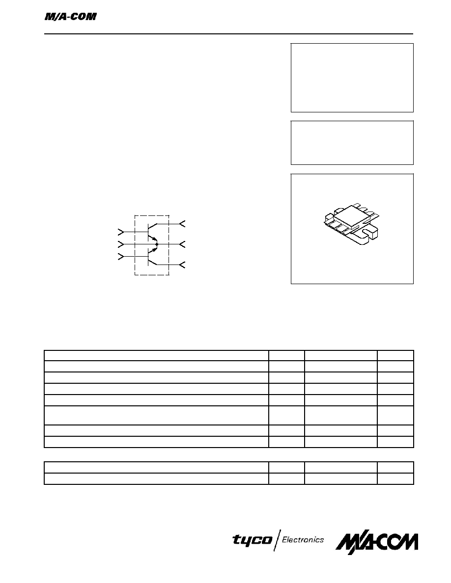
The MRF392 is two transistors in a single package with separate base and collector leads
and emitters common. This arrangement provides the designer with a space saving
device capable of operation in a push≠pull configuration.
PUSH≠PULL TRANSISTORS
MAXIMUM RATINGS
Rating
Symbol
Value
Unit
Collector≠Emitter Voltage
VCEO
30
Vdc
Collector≠Base Voltage
VCBO
60
Vdc
Emitter≠Base Voltage
VEBO
4.0
Vdc
Collector Current -- Continuous
IC
16
Adc
Total Device Dissipation @ TC = 25
∞
C (1)
Derate above 25
∞
C
PD
270
1.54
Watts
W/
∞
C
Storage Temperature Range
Tstg
≠ 65 to +150
∞
C
Junction Temperature
TJ
200
∞
C
THERMAL CHARACTERISTICS
Characteristic
Symbol
Max
Unit
Thermal Resistance, Junction to Case
R
JC
0.65
∞
C/W
NOTE:
1. This device is designed for RF operation. The total device dissipation rating applies only when the device is operated as an RF push≠pull
amplifier.
MRF392
125 W, 30 to 500 MHz
CONTROLLED "Q"
BROADBAND PUSH≠PULL
RF POWER TRANSISTOR
NPN SILICON
CASE 744A≠01, STYLE 1
Order this document
by MRF392/D
SEMICONDUCTOR TECHNICAL DATA
1
REV 8
ELECTRICAL CHARACTERISTICS
(TC = 25
∞
C unless otherwise noted)
Characteristic
Symbol
Min
Typ
Max
Unit
OFF CHARACTERISTICS (1)
Collector≠Emitter Breakdown Voltage (IC = 50 mAdc, IB = 0)
V(BR)CEO
30
--
--
Vdc
Collector≠Emitter Breakdown Voltage (IC = 50 mAdc, VBE = 0)
V(BR)CES
60
--
--
Vdc
Emitter≠Base Breakdown Voltage (IE = 5.0 mAdc, IC = 0)
V(BR)EBO
4.0
--
--
Vdc
Collector Cutoff Current (VCB = 30 Vdc, IE = 0)
ICBO
--
--
5.0
mAdc
ON CHARACTERISTICS (1)
DC Current Gain (IC = 1.0 Adc, VCE = 5.0 Vdc)
hFE
40
60
100
--
DYNAMIC CHARACTERISTICS (1)
Output Capacitance (VCB = 28 Vdc, IE = 0, f = 1.0 MHz)
Cob
--
75
95
pF
FUNCTIONAL TESTS (2) -- See Figure 1
Common≠Emitter Amplifier Power Gain
(VCC = 28 Vdc, Pout = 125 W, f = 400 MHz)
Gpe
8.0
10
--
dB
Collector Efficiency
(VCC = 28 Vdc, Pout = 125 W, f = 400 MHz)
50
55
--
%
Load Mismatch
(VCC = 28 Vdc, Pout = 125 W, f = 400 MHz,
VSWR = 30:1, all phase angles)
No Degradation in Output Power
NOTES:
1. Each transistor chip measured separately.
2. Both transistor chips operating in push≠pull amplifier.
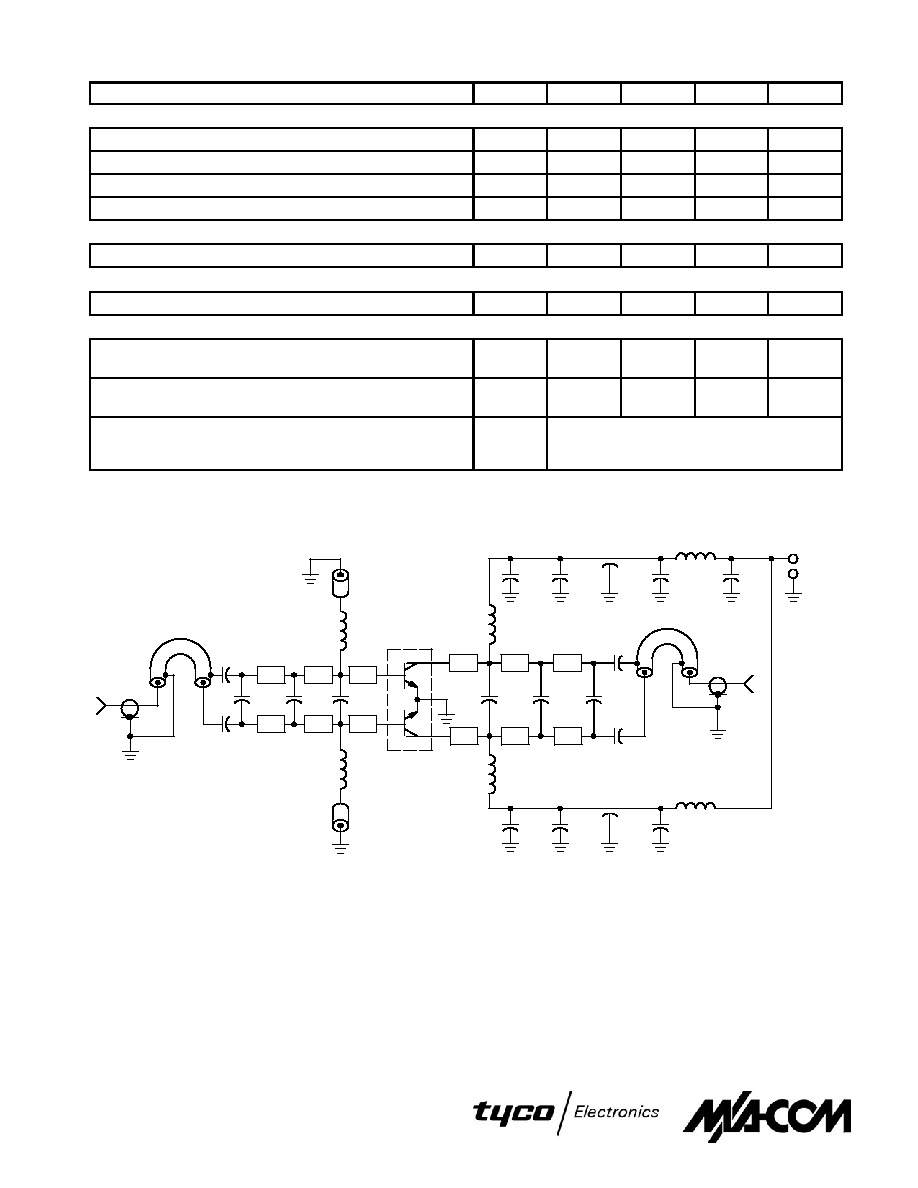
Figure 1. 400 MHz Test Fixture
D.U.T.
Z1
Z3
C9
C11
L5
Z4
Z5
L6
C16
C7
C6
C5
C3
≠
+ 28 V
L3
L4
C2
C1
Z1
Z3
Z6
Z4
Z5
Z6
C12
C13
C14
C15
B1
B2
L1
C17
C18
C19
C10
+
L2
C8
Z2
C4
Z2
C1, C2 -- 240 pF, 100 Mil Chip Cap (ATC) or Equivalent
C3 -- 3.6 pF, 100 Mil Chip Cap (ATC) or Equivalent
C4, C8 -- 8.2 pF, 100 Mil Chip Cap (ATC) or Equivalent
C5, C6 -- 20 pF, 100 Mil Chip Cap (ATC) or Equivalent
C7 -- 18 pF, Mini Unelco or Equivalent
C9, C10 -- 270 pF, 100 Mil Chip Cap (ATC) or Equivalent
C11, C12, C16, C17 -- 470 pF 100 Mil Chip Cap (ATC) or Equivalent
C13, C18 -- 680 pF Feedthru
C14, C19 -- 0.1
µ
F Erie Redcap or Equivalent
C15 -- 20
µ
F, 50 V
L1, L2 -- 0.15
µ
H Molded Choke With Ferrite Bead
L3, L4 -- 2≠1/2 Turns #20 AWG, 0.200 ID
L5, L6 -- 3≠1/2 Turns #18 AWG, 0.200 ID
B1 -- Balun, 50
Semi≠Rigid Coaxial Cable 86 Mil OD, 2
L
B2 -- Balun, 50
Semi≠Rigid Coaxial Cable 86 Mil OD, 2
L
Z1 -- Microstrip Line 270 Mil L x 125 Mil W
Z2 -- Microstrip Line 375 Mil L x 125 Mil W
Z3 -- Microstrip Line 280 Mil L x 125 Mil W
Z4 -- Microstrip Line 300 Mil L x 125 Mil W
Z5 -- Microstrip Line 350 Mil L x 125 Mil W
Z6 -- Microstrip Line 365 Mil L x 125 Mil W
Board Material -- 0.0625
Teflon Fiberglass
r = 2.5
±
0.05 1 oz. Cu.
Board Material --
CLAD, Double Sided
2
REV 8
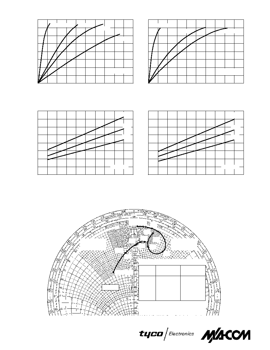
Figure 2. Output Power versus Input Power
Figure 3. Output Power versus Input Power
Figure 4. Output Power versus Supply Voltage
Figure 5. Output Power versus Supply Voltage
Figure 6. Series Equivalent Input/Output Impedance
P
, OUTPUT
POWER
(W
A
TTS)
out
80
Pin, INPUT POWER (WATTS)
0
0
4
8
12
16
20
VCC = 13.5 V
Pin = 10 W
VCC, SUPPLY VOLTAGE (VOLTS)
Pin = 14 W
f = 100 MHz
VCC = 28 V
225 MHz
400 MHz
225 MHz
500 MHz
400 MHz
P
, OUTPUT
POWER
(W
A
TTS)
out
160
Pin, INPUT POWER (WATTS)
0
140
120
100
80
0
5
10
15
20
25
60
40
20
VCC, SUPPLY VOLTAGE (VOLTS)
10
30
0
70
60
50
40
30
20
10
2
6
10
14
18
P
, OUTPUT
POWER
(W
A
TTS)
out
160
140
120
100
80
60
40
20
14
18
22
26
12
16
20
24
28
10
30
0
P
, OUTPUT
POWER
(W
A
TTS)
out
160
140
120
100
80
60
40
20
14
18
22
26
12
16
20
24
28
f = 100 MHz
5 W
7 W
7 W
10 W
f = 225 MHz
f = 400 MHz
Zin
ZOL*
225
VCC = 28 V, Pout = 125 W
f = 100 MHz
450
400
500
400
225
f = 100 MHz
Zo = 20
500
450
ZOL* = Conjugate of the optimum load impedance
ZOL* =
into which the device output operates at a
ZOL* =
given output power, voltage and frequency.
f
MHz
Zin
OHMS
ZOL*
OHMS
100
225
400
450
500
0.72 + j0.44
0.72 + j2.62
3.88 + j5.72
3.84 + j2.8
1.26 + j3.01
9.0 ≠ j6.0
5.2 ≠ j1.8
3.6 + j0.53
3.2 + j1.2
3.0 + j2.0
CAPACITIVE
REACTANCE
COMPONENT (≠jX)
INDUCTIVE
REACTANCE
COMPONENT (+jX)
Zin & ZOL* are given
from base≠to≠base and
collector≠to≠collector respectively.
3
REV 8
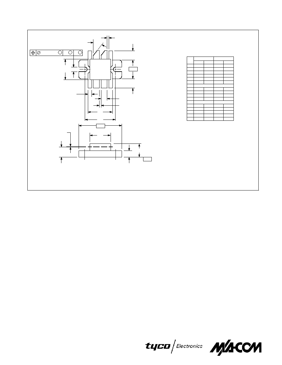
PACKAGE DIMENSIONS
CASE 744A≠01
ISSUE C
NOTES:
1. DIMENSIONING AND TOLERANCING PER ANSI
Y14.5M, 1982.
STYLE 1:
PIN 1. EMITTER (COMMON)
2. COLLECTOR
3. COLLECTOR
4. EMITTER (COMMON)
5. EMITTER (COMMON)
6. BASE
7. BASE
8. EMITTER (COMMON)
≠T≠
M
K
K
L
G
F
V
Q
4 PL
2 PL
U
4 PL
D
4 PL
R
5
6
7
8
1
2
3
4
≠B≠
M
A
M
0.76 (0.030)
B
M
≠A≠
SEATING
PLANE
N
E
C
J
H
DIM
MIN
MAX
MIN
MAX
INCHES
MILLIMETERS
A
22.60
23.11
0.890
0.910
B
9.52
10.03
0.375
0.395
C
6.65
7.16
0.262
0.282
D
1.60
1.95
0.063
0.077
E
2.94
3.40
0.116
0.134
F
2.87
3.22
0.113
0.127
G
16.51 BSC
0.650 BSC
H
4.01
4.36
0.158
0.172
J
0.07
0.15
0.003
0.006
K
4.34
4.90
0.171
0.193
L
12.45
12.95
0.490
0.510
M
45 NOM
45 NOM
N
1.051
11.02
0.414
0.434
Q
3.04
3.35
0.120
0.132
R
9.90
10.41
0.390
0.410
U
1.02
1.27
0.040
0.050
V
0.64
0.89
0.025
0.035
_
_
4
Specifications subject to change without notice.
n
North America: Tel. (800) 366-2266, Fax (800) 618-8883
n
Asia/Pacific: Tel.+81-44-844-8296, Fax +81-44-844-8298
n
Europe: Tel. +44 (1344) 869 595, Fax+44 (1344) 300 020
Visit www.macom.com for additional data sheets and product information.
REV 8