 | –≠–Ľ–Ķ–ļ—ā—Ä–ĺ–Ĺ–Ĺ—č–Ļ –ļ–ĺ–ľ–Ņ–ĺ–Ĺ–Ķ–Ĺ—ā: MAX8759 | –°–ļ–į—á–į—ā—Ć:  PDF PDF  ZIP ZIP |
General Description
The MAX8759 integrated cold-cathode fluorescent lamp
(CCFL) inverter controller is designed to drive CCFLs
using a full-bridge resonant inverter. The resonant opera-
tion ensures reliable striking and provides near-sinusoidal
waveforms over the entire input range. The controller
operates over a wide input-voltage range of 4.5V to 28V
with high power to light efficiency. The device also
includes safety features that effectively protect against
single-point fault conditions such as lamp-out, secondary
overvoltage, and secondary short-circuit faults.
The MAX8759 provides accurate lamp-current regula-
tion (
Ī2.5%) for superior CCFL inverter performance.
The lamp current is adjustable with an external resistor;
10:1 dimming range can be achieved by turning the
CCFL on and off using a digital pulse-width modulation
(DPWM) method, while maintaining the lamp-current
constant. The MAX8759 provides three mechanisms for
controlling brightness: 2-wire SMBusTM-compatible
interface, external ambient-light sensor (ALS), or sys-
tem PWM control. The MAX8759 supports Intel display
power-saving technology (DPST) to maximize battery
life. The device includes two lamp-current feedback
input pins that support dual-lamp applications with a
minimum number of external components.
The MAX8759 controls a full-bridge inverter for maxi-
mum efficiency and directly drives four external n-chan-
nel power MOSFETs. An internal 5.35V linear regulator
powers the MOSFET drivers and most of the internal
circuitry. The MAX8759 is available in a space-saving,
28-pin, thin QFN package and operates over a -40įC to
+85įC temperature range.
Applications
Notebooks
LCD Monitors
Automotive Infotainment
Features
Accurate Dimming Control Using SMBus, PWM
Interface, or Ambient Light Sensor
10:1 Dimming Range with 256-Step Resolution
Resonant-Mode Operation
Longer Lamp Life with Near Sinusoidal Lamp-
Current Waveform
Guaranteed Striking Capability
High-Power-to-Light Efficiency
Wide Input-Voltage Range (4.5V to 28V)
Input Feed-Forward for Excellent Line Rejection
Ī2.5% Lamp-Current Regulation
Adjustable 1.5% Accurate DPWM Frequency
Dual Lamp-Current Feedback Inputs
Comprehensive Fault Protection
Secondary Voltage Limiting
Primary Current Limit with Lossless Sensing
Lamp-Out Protection with Adjustable Timeout
Secondary Short-Circuit Protection
Small 28-Pin, 5mm x 5mm, Thin QFN Package
MAX8759
Low-Cost, SMBus, CCFL Backlight Controller
________________________________________________________________ Maxim Integrated Products
1
Ordering Information
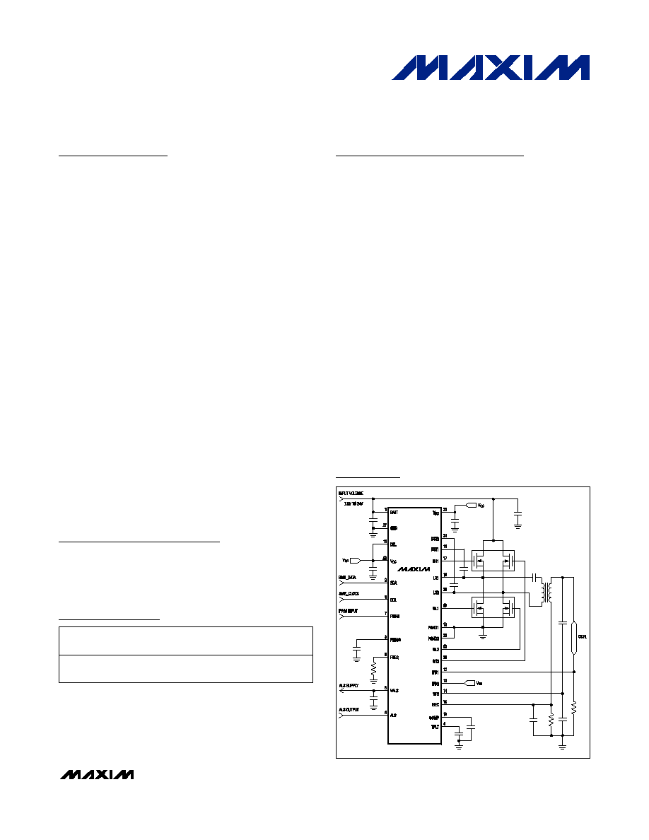
MAX8759
Minimal Operating Circuit
19-3874; Rev 1; 2/06
For pricing, delivery, and ordering information, please contact Maxim/Dallas Direct! at
1-888-629-4642, or visit Maxim's website at www.maxim-ic.com.
PART
TEMP RANGE
PIN-
PACKAGE
PKG
CODE
MAX8759ETI+
-40
įC to +85įC
28 Thin QFN-EP*
5mm
◊ 5mm
T2855-6
+ Denotes lead-free package.
*EP = Exposed pad.
Pin Configuration appears at end of data sheet.
SMBus is a trademark of Intel Corp.

MAX8759
Low-Cost, SMBus, CCFL Backlight Controller
2
_______________________________________________________________________________________
ABSOLUTE MAXIMUM RATINGS
ELECTRICAL CHARACTERISTICS
(Circuit of Figure 1, V
BATT
= 12V, V
CC
= V
DD,
T
A
= 0įC to +85įC. Typical values are at T
A
= +25
įC, unless otherwise noted.)
Stresses beyond those listed under "Absolute Maximum Ratings" may cause permanent damage to the device. These are stress ratings only, and functional
operation of the device at these or any other conditions beyond those indicated in the operational sections of the specifications is not implied. Exposure to
absolute maximum rating conditions for extended periods may affect device reliability.
BATT to GND..........................................................-0.3V to +30V
BST1, BST2 to GND ...............................................-0.3V to +36V
BST1 to LX1, BST2 to LX2 ........................................-0.3V to +6V
FREQ, V
CC
, VDD to GND .........................................-0.3V to +6V
SDA, SCL to GND.....................................................-0.3V to +6V
ALS, COMP, PWMI, PWMO,
TFLT, DEL, VALS to GND .......................-0.3V to (V
CC
+ 0.3V)
GH1 to LX1 ..............................................-0.3V to (V
BST1
+ 0.3V)
GH2 to LX2 ..............................................-0.3V to (V
BST2
+ 0.3V)
GL1, GL2 to GND .......................................-0.3V to (V
DD
+ 0.3V)
IFB1, IFB2, ISEC, VFB to GND ....................................-3V to +6V
PGND1, PGND2 to GND .......................................-0.3V to +0.3V
Continuous Power Dissipation (T
A
= +70
įC)
28-Pin Thin QFN 5mm x 5mm
(derate 21.3mW/
įC above +70įC).............................1702mW
Operating Temperature Range ...........................-40
įC to +85įC
Junction Temperature ......................................................+150
įC
Storage Temperature Range .............................-65
įC to +150įC
Lead Temperature (soldering, 10s) .................................+300
įC
PARAMETER
CONDITIONS
MIN
TYP
MAX
UNITS
V
CC
= V
DD
= V
BATT
4.5
5.5
BATT Input Voltage Range
V
CC
= V
DD
= open
5.5
28.0
V
V
BATT
= 28V
2.5
5
BATT Quiescent Current
MAX8759 is enabled
V
BATT
= V
CC
= 5V
5
mA
BATT Quiescent Current, Shutdown
MAX8759 is disabled
0.1
2
ĶA
V
CC
Output Voltage, Normal Operation
MAX8759 is enabled, 6V < V
BATT
< 28V,
0 < I
LOAD
< 10mA
5.2
5.35
5.5
V
V
CC
Output Voltage, Shutdown
MAX8759 is disabled, no load
3.5
4.3
5.5
V
V
CC
rising (leaving lockout)
4.3
V
CC
Undervoltage Lockout Threshold
V
CC
falling (entering lockout)
3.7
V
V
CC
Undervoltage Lockout Hysteresis
230
mV
V
CC
POR Threshold
Rising edge
1.75
V
V
CC
POR Hysteresis
50
mV
GH1, GH2, GL1, GL2 On-Resistance,
Low State
I
TEST
= 100mA, V
CC
= V
DD
= 5V
3
6
GH1, GH2, GL1, GL2 On-Resistance,
High State
I
TEST
= 100mA, V
CC
= V
DD
= 5V
10
18
BST1, BST2 Leakage Current
V
BST
_ = 12V, V
LX
_ = 7V
4
10
ĶA
Resonant Frequency Range
Guaranteed by design
30
80
kHz
Minimum On-Time
350
500
700
ns
Maximum Off-Time
40
60
80
Ķs
Current-Limit Threshold
LX1 - PGND1, LX2 - PGND2
415
430
445
mV
Zero-Current-Crossing Threshold
LX1 - PGND1, LX2 - PGND2
3
8
13
mV
Current-Limit Leading-Edge Blanking
350
ns
IFB1, IFB2 Input-Voltage Range
-3
+3
V
IFB1 Regulation Point
765
785
805
mV
IFB2 Regulation Point
780
800
820
mV

MAX8759
Low-Cost, SMBus, CCFL Backlight Controller
_______________________________________________________________________________________
3
ELECTRICAL CHARACTERISTICS (continued)
(Circuit of Figure 1, V
BATT
= 12V, V
CC
= V
DD,
T
A
= 0įC to +85įC. Typical values are at T
A
= +25
įC, unless otherwise noted.)
PARAMETER
CONDITIONS
MIN
TYP
MAX
UNITS
0 < V
IFB1,2
< 3V
-3
+3
IFB1, IFB2 Input Bias Current
-3V < V
IFB1,2
< 0
-230
ĶA
IFB1, IFB2 Lamp-Out Threshold
575
600
625
mV
IFB1, IFB2 to COMP Transconductance
0.5V < V
COMP
< 4V
60
100
160
ĶS
COMP Output Impedance
6
12
24
M
COMP Discharge Current During Overvoltage
or Overcurrent Fault
V
VFB
= 2.6V or V
ISEC
= 1.5V
500
1000
2000
ĶA
COMP Discharge Current During DPWM
Off-Time
V
COMP
= 1.5V
90
110
130
ĶA
DPWM Rising-to-Falling Ratio
V
IFB1,2
= 0
2.5
ISEC Input Voltage Range
-3
+3
V
ISEC Overcurrent Threshold
1.18
1.21
1.26
V
ISEC Input Bias Current
V
ISEC
= 1.25V
-0.3
+0.3
ĶA
VFB Input Voltage Range
-4
+4
V
VFB Input Impedance
150
300
450
M
VFB Overvoltage Threshold
2.2
2.3
2.4
V
VFB Undervoltage Threshold
210
240
280
mV
VFB Undervoltage Delay
R
FREQ
= 169k
250
Ķs
R
FREQ
= 169k
, T
A
= +25įC to +85įC
207
210
213
R
FREQ
= 169k
205
210
215
R
FREQ
= 340k
106
DPWM Oscillator Frequency
R
FREQ
= 100k
343
Hz
PWMO Output Impedance
20
40
60
k
PWMI Input Low Voltage
0.7
V
PWMI Input High Voltage
2.1
V
PWMI Input Hysteresis
300
mV
PWMI Input Bias Current
-0.3
+0.3
ĶA
PWMI Input Frequency Range
5
50
kHz
PWMI Full-Range Accuracy
5
LSB
PWMI duty cycle = 100%
98
100
PWMI duty cycle = 50%
48
50
52
PWMI Brightness Setting
PWMI duty cycle = 0%
9.7
10.0
10.3
%
ALS Full-Adjustment Range
0
1.8
V
ALS Full-Range Accuracy
5
LSB
ALS Input Bias Current
-0.1
+0.1
ĶA
VALS Output Voltage
MAX8759 is enabled, 6V < V
BATT
< 28V,
I
LOAD
= 1mA
5.10
5.30
5.50
V
VALS Leakage Current
MAX8759 is disabled, VALS = GND
-3
+3
ĶA
VALS On-Resistance
MAX8759 is enabled
30
60

MAX8759
Low-Cost, SMBus, CCFL Backlight Controller
4
_______________________________________________________________________________________
ELECTRICAL CHARACTERISTICS (continued)
(Circuit of Figure 1, V
BATT
= 12V, V
CC
= V
DD,
T
A
= 0įC to +85įC. Typical values are at T
A
= +25
įC, unless otherwise noted.)
PARAMETER
CONDITIONS
MIN
TYP
MAX
UNITS
V
BATT
= 9V, R
THR
= 120k
0
0.15
0.30
Zero-Crossing Delay
V
BATT
= 12V, R
THR
= 120k
1.50
1.80
2.10
Ķs
Maximum Zero-Crossing Delay
V
BATT
= 18V, R
THR
= 120k
3.2
3.8
4.4
Ķs
DEL rising
4.5
DEL Disable Threshold
DEL falling
3.8
V
V
ISEC
< 1.25V and V
IFB
< 540mV; V
FLT
= 2V
0.9
1.0
1.1
V
ISEC
< 1.25V and V
IFB
> 660mV; V
FLT
= 2V
-1.5
-1.2
-0.8
TFLT Charge Current
V
ISEC
> 1.25V and V
IFB
> 660mV; V
FLT
= 2V
115
135
155
ĶA
TFLT Trip Threshold
Rising edge
3.7
4
4.3
V
SDA, SCL, Input Low Voltage
0.7
V
SDA, SCL, Input High Voltage
2.1
V
SDA, SCL, Input Hysteresis
100
mV
SDA, SCL, Input Bias Current
-1
+1
ĶA
SDA Output Low Sink Current
V
SDA
= 0.4V
4
mA
SMBus Frequency
10
100
kHz
SMBus Free Time
t
BUF
4.7
1
Ķs
SCL Serial Clock High Period
t
HIGH
4
Ķs
SCL Serial Clock Low Period
t
LOW
4.7
Ķs
START Condition Setup Time
t
SU:STA
4.7
Ķs
START Condition Hold Time
t
HD:STA
4
Ķs
STOP Condition Setup Time from SCL
t
SU:STO
4
Ķs
SDA Valid to SCL Rising-Edge Setup Time,
Slave Clocking in Data
t
SU:DAT
250
ns
SCL Falling Edge to SDA Transition
t
HD:DAT
0
ns
SCL Falling Edge to SDA Valid, Reading Out
Data
t
DV
200
ns

MAX8759
Low-Cost, SMBus, CCFL Backlight Controller
_______________________________________________________________________________________
5
ELECTRICAL CHARACTERISTICS
(Circuit of Figure 1, V
BATT
= 12V, V
CC
= V
DD,
T
A
= -40įC to +85įC.) (Note 1)
PARAMETER
CONDITIONS
MIN
TYP
MAX
UNITS
V
CC
= V
DD
= V
BATT
4.5
5.5
BATT Input Voltage Range
V
CC
= V
DD
= open
5.5
28.0
V
V
BATT
= 28V
5
BATT Quiescent Current
MAX8759 is enabled
V
BATT
= V
CC
= 5V
5
mA
V
CC
Output Voltage, Normal Operation
MAX8759 is enabled, 6V < V
BATT
< 28V,
0 < I
LOAD
< 10mA
5.2
5.5
V
V
CC
Output Voltage, Shutdown
MAX8759 is disabled, no load
3.5
5.5
V
V
CC
rising (leaving lockout)
4.3
V
CC
Undervoltage Lockout Threshold
V
CC
falling (entering lockout)
3.7
V
GH1, GH2, GL1, GL2 On-Resistance,
Low State
I
TEST
= 100mA, V
CC
= V
DD
= 5V
6
GH1, GH2, GL1, GL2 On-Resistance,
High State
I
TEST
= 100mA, V
CC
= V
DD
= 5V
18
Resonant Frequency Range
Guaranteed by design
30
80
kHz
Minimum On-Time
350
700
ns
Maximum Off-Time
40
80
Ķs
Current-Limit Threshold
LX1 - PGND1, LX2 - PGND2
410
450
mV
Zero-Current Crossing Threshold
LX1 - PGND1, LX2 - PGND2
3
13
mV
IFB1, IFB2 Input Voltage Range
-3
+3
V
IFB1 Regulation Point
760
810
mV
IFB2 Regulation Point
775
825
mV
IFB1, IFB2 Input Bias Current
-3V < V
IFB1,2
< 0
-230
ĶA
IFB1, IFB2 Lamp-Out Threshold
565
635
mV
IFB1, IFB2 to COMP Transconductance
0.5V < V
COMP
< 4V
60
160
ĶS
COMP Output Impedance
6
25
M
COMP Discharge Current During Overvoltage
or Overcurrent Fault
V
VFB
= 2.6V or V
ISEC
= 1.5V
500
2000
ĶA
COMP Discharge Current During DPWM
Off-Time
V
COMP
= 1.5V
90
130
ĶA
ISEC Input Voltage Range
-3
+3
V
ISEC Overcurrent Threshold
1.18
1.26
V
VFB Input Voltage Range
-4
+4
V
VFB Input Impedance
150
450
M
VFB Overvoltage Threshold
2.2
2.4
V
VFB Undervoltage Threshold
210
280
mV
DPWM Oscillator Frequency
R
FREQ
= 169k
203
217
Hz
PWMO Output Impedance
20
60
k