
T
TT
T
TOSHIB
OSHIB
OSHIB
OSHIB
OSHIBA Bi-CMOS
A Bi-CMOS
A Bi-CMOS
A Bi-CMOS
A Bi-CMOS
Constant Cur
Constant Cur
Constant Cur
Constant Cur
Constant Currrrrrent Interf
ent Interf
ent Interf
ent Interf
ent Interface Dri
ace Dri
ace Dri
ace Dri
ace Drivvvvver
er
er
er
er
For up-to-date product info visit our web site at www.marktechopto.com All specifications subject to change.
TB62705CP/CF/CFN
8 Bit Constant Current LED Driver with
Shift Register and Latch Functions
Product Description:
The TB62705CP/CF/CFN is specifically designed
for LED display applications. The Bi-CMOS device
has 8 Bi-Polar constant current output channels
and includes CMOS shift register and latch
functions.
The LED drive current is programmed by the
installation of a single resistor per device. Current
is programmable from 5-90mA and is held
constant across all 8 outputs effectively compen-
sating for the inherent circuit and component
variables which affect the brightness of the LEDs.
Features:
� 8 Constant Current Output Channels
� Current Programmable from 5-90mA
� 5V CMOS Compatible Inputs
� 15MHz Max Clock Frequency (Cascade)
Block Diagram:
SSOP16-P-225-1.00A
TB62705CF
Weight: 0.14g(typ)
SSOP16-P-225-0.65B
TB62705CFN
Weight: 0.07g(typ)
NEW! Ultra Small Surface Mount Package
DIP16-P-300-2.54A
TB62705CP
Weight: 1.11g(typ)
Company Headquarters
3 Northway Lane North
Latham, New York 12110
Toll Free: 800.984.5337
Fax:
518.785.4725
Web: www.marktechopto.com | Email: info@marktechopto.com
California Sales Office:
950 South Coast Drive, Suite 265
Costa Mesa, California 92626
Toll Free: 800.984.5337
Fax: 714.850.9314

T
TT
T
TOSHIB
OSHIB
OSHIB
OSHIB
OSHIBA Bi-CMOS
A Bi-CMOS
A Bi-CMOS
A Bi-CMOS
A Bi-CMOS
Constant Cur
Constant Cur
Constant Cur
Constant Cur
Constant Currrrrrent Interf
ent Interf
ent Interf
ent Interf
ent Interface Dri
ace Dri
ace Dri
ace Dri
ace Drivvvvver
er
er
er
er
For up-to-date product info visit our web site at www.marktechopto.com All specifications subject to change.
TB62705CP/CF/CFN
Timing Diagram:
Terminal Description & Pin Out:
PIN No.
PIN NAME
FUNCTION
1
GND
GND terminal for control logic
2
SERIAL-IN
Input terminal of a serial-data for shift register
3
CLOCK
Input terminal of a clock for data shift up to edge.
4
LATCH
Inout terminal of a data strobe. (Latches pass data with "H" level inputof
LATCH-terminal, and hold data with "L" level input.)
5~12
OUT0~7
Output terminals
13
ENABLE
Input Teminal of output enable. (All outputs (OUT0~7) do off with "H" level
input of ENABLE terminal, and on with "L"level input.)
14
SERIAL-OUT
Output terminal of serial data for next SERIAL-IN terminal.
15
R-EXT
Constant Current Programming through external resistor
16
VDD
5V Supply voltage terminal
Latches are:
1. Level Sesitive
2. Not edge sensitive
3. Not clock synchronous
4. Passing Data when LATCH is H
5. Hold Data when LATCH is L
All Outputs are OFF when ENABLE is H and ON when ENABLE is L.
Company Headquarters
3 Northway Lane North
Latham, New York 12110
Toll Free: 800.984.5337
Fax:
518.785.4725
Web: www.marktechopto.com | Email: info@marktechopto.com
California Sales Office:
950 South Coast Drive, Suite 265
Costa Mesa, California 92626
Toll Free: 800.984.5337
Fax: 714.850.9314

T
TT
T
TOSHIB
OSHIB
OSHIB
OSHIB
OSHIBA Bi-CMOS
A Bi-CMOS
A Bi-CMOS
A Bi-CMOS
A Bi-CMOS
Constant Cur
Constant Cur
Constant Cur
Constant Cur
Constant Currrrrrent Interf
ent Interf
ent Interf
ent Interf
ent Interface Dri
ace Dri
ace Dri
ace Dri
ace Drivvvvver
er
er
er
er
For up-to-date product info visit our web site at www.marktechopto.com All specifications subject to change.
TB62705CP/CF/CFN
Truth Table:
Equivalent Circuit of Inputs and Outputs:
Maximum Ratings:
CLOCK
LATCH
ENABLE
SERIAL-IN
OUT0 OUT5 OUT7
SERIAL-OUT
UP
H
L
Dn
Dn Dn-5 Dn-7
Dn-7
UP
L
L
Dn+1
No Change
Dn-6
UP
H
L
Dn+2
Dn+2 Dn-3 Dn-5
Dn-5
DOWN
X
L
Dn+3
Dn+2 Dn-3 Dn-5
Dn-5
DOWN
X
H
DN+3
Off
Dn-5
CHARACTER
SYMBOL
RATING
UNIT
Supply Voltage
VDD
0~+7.0
V
Input Voltage
VIN
-0.4~VDD + 0.4
V
Output Current
IOUT
+90
mA
Output Voltage
VOUT
-0.5~+17.0
V
Clock Frequency
FCLK
15
MHz
GND Terminal Current
IGND
720
mA
Power Dissipation
PD
1.47 (CP type : FREE AIR,Ta=25�C)
W
0.78 (CF/CFN type : ON PCB,Ta=25�C)
Thermal Resistance
Rth (j-a)
85 (CP type : FREE AIR,Ta=25�C)
�C / W
160 (CF/CFN type : ON PCB,Ta=25�C)
Operating Temperature
Topr
-40~+85
�C
Storage Temperature
Tstg
-55~+150
�C
Company Headquarters
3 Northway Lane North
Latham, New York 12110
Toll Free: 800.984.5337
Fax:
518.785.4725
Web: www.marktechopto.com | Email: info@marktechopto.com
California Sales Office:
950 South Coast Drive, Suite 265
Costa Mesa, California 92626
Toll Free: 800.984.5337
Fax: 714.850.9314

T
TT
T
TOSHIB
OSHIB
OSHIB
OSHIB
OSHIBA Bi-CMOS
A Bi-CMOS
A Bi-CMOS
A Bi-CMOS
A Bi-CMOS
Constant Cur
Constant Cur
Constant Cur
Constant Cur
Constant Currrrrrent Interf
ent Interf
ent Interf
ent Interf
ent Interface Dri
ace Dri
ace Dri
ace Dri
ace Drivvvvver
er
er
er
er
For up-to-date product info visit our web site at www.marktechopto.com All specifications subject to change.
TB62705CP/CF/CFN
Recommended Operating Condition:
CHARACTERISTIC
SYMBOL
CONDITION
MIN.
TYP.
MAX.
UNIT
Supply Voltage
VDD
4.5
5.0
5.5
V
Outout Voltage
VOUT
--
--
15.0
V
Output Current
IOUT
DC 1 Circuit
5
--
88
mA
IOH
SERIAL-OUT
--
--
-1.0
mA
IOL
SERIAL-OUT
--
--
1.0
mA
Input Voltage
VIH
0.7VDD
--
VDD+0.3
V
VIL
-0.3
--
0.3VDD
V
LATCH Pulse Width
tw LAT
VDD=4.5 ~ 5.5V
100
--
--
ns
CLOCK Pulse Width
tw CLK
50
--
--
ns
ENABLE Pulse Width
tw EN
4500
--
--
ns
Set-up Time for DATA
tsetup(D)
60
--
--
ns
Hold Time for Data
thold(D)
20
--
--
ns
Set-up Time for LATCH
tsetup(L)
100
--
--
ns
Hold Time for ENABLE
thold(L)
60
--
--
ns
Clock Frequency
FCLK
Cascade Operation
1
--
--
MHz
Power Dissipation
PD
Ta=85�C (CP type FREE AIR)
--
--
0.82
W
Ta=85�C (CF/CFN type ON PCB)
--
--
0.40
Company Headquarters
3 Northway Lane North
Latham, New York 12110
Toll Free: 800.984.5337
Fax:
518.785.4725
Web: www.marktechopto.com | Email: info@marktechopto.com
California Sales Office:
950 South Coast Drive, Suite 265
Costa Mesa, California 92626
Toll Free: 800.984.5337
Fax: 714.850.9314
T
TT
T
TOSHIB
OSHIB
OSHIB
OSHIB
OSHIBA Bi-CMOS
A Bi-CMOS
A Bi-CMOS
A Bi-CMOS
A Bi-CMOS
Constant Cur
Constant Cur
Constant Cur
Constant Cur
Constant Currrrrrent Interf
ent Interf
ent Interf
ent Interf
ent Interface Dri
ace Dri
ace Dri
ace Dri
ace Drivvvvver
er
er
er
er
For up-to-date product info visit our web site at www.marktechopto.com All specifications subject to change.
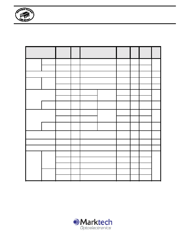
CHARACTERISTIC
SYMBOL
TEST
CIR-
CUIT
CONDITION
MIN.
TYP.
MAX.
UNIT
Input
Voltage
"H" level
VIH
--
--
0.7VDD
--
VDD
V
"L" level
VIL
--
--
GND
--
0.3VDD
Output Leakage Current
IOH
--
VOH=15.0V
--
--
10
�A
Output
Voltage
SERIAL--
OUT
VOL
--
IOL=+1.0mA
--
--
0.4
V
VOH
--
IOH=-1.0mA
4.6
--
--
V
Output Current 1
IOL1
--
VCE=0.7V
REXT=470
(include Skew)
34.1
40.0
45.9
mA
IOL2
--
VCE=0.4V
33.7
39.5
45.3
Current
Skew
dIOL1
--
IO=40mA,
VCE=0.4V
REXT=470
--
�1.5
�6.0
%
Output Current 2
IOL3
VCE=0.4V
REXT=250
(Include Skew)
64.2
75.5
86.8
mA
IOL4
VCE=0.7V
63.8
75.0
86.2
Current
Skew
dIOL2
IO=75mA,
VCE=0.7V
REXT=250
�1.5
�6.0
%
Supply Voltage
Regulation
% / VDD
--
REXT=470
Ta=~+85�C
--
�1.5
�5.0
% /V
Pull Up Resistor
RIN(up)
--
--
150
300
600
K
Pull-down Resistor
RIN(down)
--
--
100
200
400
K
Supply
Current
"OFF"
IIDD (off) 1
--
REXT=OPEN OUT 1~8=off
--
0.6
1.2
mA
IIDD (off) 2
--
REXT=470
OUT 1~8=off
3.5
5.8
8.0
IIDD (off) 3
--
REXT=250
OUT 1~8=off
6.5
10.7
15.0
"ON"
IDD (on)1
--
REXT=470
OUT 1~8=on
7.0
12.0
18.0
IDD (on)2
--
REXT=250
OUT 1~8=on
10.0
22.0
32.0
Electrical Characteristics:
TB62705CP/CF/CFN
Company Headquarters
3 Northway Lane North
Latham, New York 12110
Toll Free: 800.984.5337
Fax:
518.785.4725
Web: www.marktechopto.com | Email: info@marktechopto.com
California Sales Office:
950 South Coast Drive, Suite 265
Costa Mesa, California 92626
Toll Free: 800.984.5337
Fax: 714.850.9314