
TB62726ANG/AFG
TOSHIBA Bi-CMOS Integrated Circuit Silicon Monolithic
TB62726ANG,TB62726AFG
16-bit Constant-Current LED Driver with Operating Voltage of 3.3-V and 5-V
The TB62726A series are comprised of constant-current drivers
designed for LEDs and LED displays. The output current value
can be set using an external resistor.
As a result, all outputs will have virtually the same current
levels.
This driver incorporates 16-bit constant-current outputs, a
16-bit shift register, a 16-bit latch and a 16-bit AND-gate circuit.
These drivers have been designed using the Bi-CMOS process.
This devices are a product for the Pb free.
Features
∑ Output current capability and number of outputs:
90 mA
◊ 16 outputs
∑ Constant current range: 2 to 90 mA
∑ Application output voltage: 0.7 V (output current 2 to 80 mA)
0.4 V (output current 2 to 40 mA)
∑ For anode-common LEDs
∑ Input signal voltage level: 3.3-V and 5-V CMOS level (Schmitt
trigger input)
∑ Power supply voltage range V
DD
= 3.0 to 5.5 V
∑ Maximum output terminal voltage: 17 V
∑ Serial and parallel data transfer rate: 20 MHz (max, cascade
connection)
∑ Operating temperature range T
opr
= -40 to 85∞C
∑ Package: Type ANG: SDIP24-P-300-1.78
Type
AFG:
SSOP24-P-300-1.00B
∑ Current accuracy (All output ON)
Current Accuracy
Output Voltage
Between Bits
Between ICs
Output Current
>
=
0.4 V
±
15%
2 to 5 mA
>
=
0.7 V
±
4%
±
12%
5 to 80 mA
TB62726ANG
TB62726AFG
Weight
SDIP24-P-300-1.78: 1.22 g (typ.)
SSOP24-P-300-1.00B: 0.32 g (typ.)
Web: www.marktechopto.com | Email: info@marktechopto.com
Company Headquarters
3 Northway Lane North
Latham, New York 12110
Toll Free: 800.984.5337
Fax:
518.785.4725
California Sales Office:
950 South Coast Drive, Suite 2
25
Costa Mesa, California 92626
Toll Free: 800.984.5337
Fax: 714.850.9314

TB62726ANG/AFG
2005-12-21
2
Pin Assignment
(top view)
Warnings: Short-circuiting an output terminal to GND or to the power supply terminal may broken the device.
Please take care when wiring the output terminals, the power supply terminal and the GND terminals.
Block Diagram
Truth Table
CLOCK
LATCH
ENABLE SERIAL-IN
OUT0
...
OUT7
...
OUT15 SERIAL-OUT
H L
Dn Dn
...
Dn
-
7
...
Dn
-
15
Dn
-
15
L L
Dn
+
1
No change
Dn
-
14
H L
Dn
+
2
Dn
+
2
...
Dn
-
5
...
Dn
-
13
Dn
-
13
X L
Dn
+
3
Dn
+
2
...
Dn
-
5
...
Dn
-
13
Dn
-
13
X H
Dn
+
3
OFF
Dn
-
13
Note 1: OUT0 to OUT15
=
On when Dn
=
H; OUT0 to OUT15
=
Off when Dn
=
L.
In order to ensure that the level of the power supply voltage is correct, an external resistor must be connected
between R-EXT and GND.
GND
SERIAL-IN
LATCH
CLOCK
OUT0
OUT1
OUT2
OUT3
V
DD
R-EXT
SERIAL-OUT
ENABLE
OUT15
OUT14
OUT13
OUT12
OUT4
OUT5
OUT6
OUT7
OUT11
OUT10
OUT9
OUT8
SERIAL-IN
LATCH
OUT0
R-EXT
ENABLE
I-REG
Q
ST D
Q
ST D
D Q
CK
Q
ST D
D Q
CK
D Q
CK
CLOCK
OUT1
OUT15
SERIAL-OUT

TB62726ANG/AFG
2005-12-21
3
Timing Diagram
Warning: Latch circuit is leveled-latch circuit. Be careful because it is not triggered-latch circuit.
Note 2: The latches circuit holds data by pulling the LATCH terminal Low.
And, when LATCH terminal is a High level, latch circuit doesn't hold data, and it passes from the input to
the output.
When ENABLE terminal is a Low level, output terminal OUT0 to OUT15 respond to the data, and on
and off does.
And, when ENABLE terminal is a High level, it offs with the output terminal regardless of the data.
SERIAL-IN
LATCH
CLOCK
OUT0
OUT1
OUT3
SERIAL-OUT
ENABLE
OUT15
3.3 V/5 V
0 V
n
=
0 1
2
3
4
5
6
8
3.3 V/5 V
0 V
3.3 V/5 V
0 V
3.3 V/5 V
0 V
On
Off
On
Off
On
Off
On
Off
3.3 V/5 V
0 V
7
9
11
10
12
14
13
15

TB62726ANG/AFG
2005-12-21
4
Terminal Description
Pin No.
Pin Name
Function
1
GND
GND terminal for control logic
2
SERIAL-IN
Input terminal for serial data for data shift register
3
CLOCK
Input terminal for clock for data shift on rising edge
4
LATCH
Input terminal for data strobe
When the LATCH input is driven High, data is not latched. When it is pulled Low, data is
latched.
5 to 20
OUT0 to OUT15 Constant-current output terminals
21
ENABLE
Input terminal for output enable.
All outputs ( OUT0 to OUT15 ) are turned off, when the ENABLE terminal is driven High.
And are turned on, when the terminal is driven Low.
22
SERIAL-OUT
Output terminal for serial data input on SERIAL-IN terminal
23
R-EXT
Input terminal used to connect an external resistor. This regulated the output current.
24 V
DD
3.3-V/5-V supply voltage terminal
Equivalent Circuits for Inputs and Outputs
1. ENABLE terminal
2. LATCH terminal
3. CLOCK, SERIAL-IN terminal
4. SERIAL-OUT terminal
5. OUT0 to OUT15 terminals
V
DD
ENABLE
GND
R (UP)
V
DD
LATCH
GND
R (DOWN)
CLOCK,
SERIAL-IN
V
DD
GND
V
DD
GND
Internal data
SERIAL-OUT
Parasitic Diode
OUT0 to OUT15
GND
TB62726ANG/AFG
2005-12-21
5
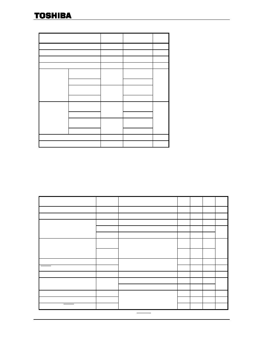
Maximum Ratings
(T
opr
=
25∞C)
Characteristics Symbol
Rating
Unit
Supply voltage
V
DD
6 V
Input voltage
V
IN
-
0.2 to V
DD
+
0.2
V
Output current
I
OUT
+
90 mA/ch
Output voltage
V
OUT
-
0.2 to 17
V
ANG-type
(when not mounted)
1.25
ANG-type (on PCB)
P
d1
1.78
AFG-type
(when not mounted)
0.83
Power dissipation
(Note 3)
AFG-type (on PCB)
P
d2
1.00
W
ANG-type
(when not mounted)
104
ANG-type (on PCB)
R
th (j-a) 1
70
AFG-type
(when not mounted)
140
Thermal resistance
(Note 3)
AFG-type (on PCB)
R
th (j-a) 2
120
∞C/W
Operating temperature
T
opr
-
40 to 85
∞C
Storage temperature
T
stg
-
55 to 150
∞C
Note 3: ANG-Type: Powers dissipation is derated by 14.28 mW/∞C if device is mounted on PCB and ambient
temperature is above 25∞C.
AFG-Type: Powers dissipation is derated by 6.67 mW/∞C if device is mounted on PCB and ambient
temperature is above 25∞C.
With device mounted on glass-epoxy PCB of less than 40% Cu and of dimensions
50 mm
◊
50 mm
◊
1.6 mm.
Recommended Operating Conditions
(T
opr
=
-
40∞C to 85∞C unless otherwise specified)
Characteristics Symbol
Conditions Min
Typ.
Max
Unit
Supply voltage
V
DD
3
5.5 V
Output voltage
V
OUT
0.7 4 V
I
OUT
Each DC 1 circuit
2
80
mA/ch
I
OH
SERIAL-OUT
-
1
Output current
I
OL
SERIAL-OUT
1
mA
V
IH
0.7
◊
V
DD
V
DD
+
0.15
Input voltage
V
IL
-
0.15
0.3
◊
V
DD
V
Clock frequency
f
CLK
20 MHz
LATCH pulse width
t
wLAT
Cascade connected
50
ns
CLOCK pulse width
t
wCLK
25
ns
Upper I
OUT
=
20 mA
2000
ENABLE pulse width
(Note 4)
t
wENA
Lower I
OUT
=
20 mA
3000
ns
Set-up time for CLOCK terminal
t
SETUP1
10
ns
Hold time for CLOCK terminal
t
HOLD
10
ns
Set-up time for LATCH terminal
t
SETUP2
50
ns
Note 4: When the pulse of the Low level is inputted to the ENABLE terminal held in the High level.

TB62726ANG/AFG
2005-12-21
6
Electrical Characteristics
(T
opr
=
25∞C, V
DD
=
3.0 V to 5.5 V unless otherwise specified)
Characteristics Symbol
Conditions Min
Typ.
Max
Unit
Supply voltage
V
DD
Normal
operation
3.0
5.5 V
I
OUT1
V
OUT
=
0.4 V,
V
DD
=
3.3 V
31.96 36.20 40.54
I
OUT2
V
OUT
=
0.4 V,
V
DD
=
5 V
R
EXT
=
490
31. 59 35.90 40.20
I
OUT3
V
OUT
=
0.7 V,
V
DD
=
3.3 V
63.63 72.30 80.97
Output current
I
OUT4
V
OUT
=
0.7 V,
V
DD
=
5 V
R
EXT
=
250
62.75 71.30 79.95
mA
I
OUT1
V
OUT
0.4 V,
All outputs ON
R
EXT
=
490
Output current error between bits
I
OUT2
V
OUT
0.4 V,
All outputs ON
R
EXT
=
250
±
1
±
4 %
Output leakage current input voltage
I
OZ
V
OUT
=
15.0 V
1
µ
A
0.7
V
DD
V
DD
Input voltage
V
IN
GND
0.3
V
DD
V
I
OL
=
1.0 mA, V
DD
=
3.3 V
0.3
V
OL
I
OL
=
1.0 mA, V
DD
=
5 V
0.3
I
OH
=
-
1.0 mA, V
DD
=
3.3 V
3
SOUT terminal voltage
V
OH
I
OH
=
1.0 mA, V
DD
=
5 V
4.7
V
Output current
Supply voltage
Regulation
%/V
DD
When
V
DD
is changed 3 V to 5.5 V
-
1
-
5 %
Pull-up resistor
R
(Up)
ENABLE terminal
Pull-down resistor
R
(Down)
LATCH terminal
115 230 460 k
I
DD (OFF) 1
V
OUT
=
15.0 V
R
EXT
=
OPEN
0.1 0.5
I
DD (OFF) 2
V
OUT
=
15.0 V,
All outputs OFF
R
EXT
=
490
1 3.5 5
I
DD (OFF) 3
V
OUT
=
15.0 V,
All outputs OFF
R
EXT
=
250
4 6 9
V
OUT
=
0.7 V,
All outputs ON
R
EXT
=
490
9 15
I
DD (ON) 1
Same as the above, T
opr
=
-
40∞C
20
V
OUT
=
0.7 V,
All outputs ON
R
EXT
=
250
18 25
Supply current
I
DD (ON) 2
Same as the above, T
opr
=
-
40∞C
40
mA

TB62726ANG/AFG
2005-12-21
7
Switching Characteristics
(T
opr
=
25∞C unless otherwise specifed
)
Characteristics Symbol
Conditions Min
Typ.
Max
Unit
t
pLH1
CLK- OUTn ,
LATCH
=
"H",
ENABLE
=
"L"
150 300
t
pLH2
LATCH - OUTn ,
ENABLE
=
"L"
140 300
t
pLH3
ENABLE - OUTn ,
LATCH
=
"H"
140 300
t
pLH
CLK-SERIAL
OUT
3 6
t
pHL1
CLK- OUTn , LATCH
=
"H",
ENABLE
=
"L"
170 340
t
pHL2
LATCH - OUTn ,
ENABLE
=
"L"
170 340
t
pHL3
ENABLE - OUTn ,
LATCH
=
"H"
170 340
Propagation delay
t
pLH
CLK-SERIAL
OUT
4 7
ns
Output rise time
t
or
10 to 90% of voltage waveform
40
85
150
ns
Output fall time
t
of
90 to 10% of voltage waveform
40
70
150
ns
Maximum CLOCK rise time
t
r
5
µ
s
Maximum CLOCK fall time
t
f
When not on PCB
(Note 5)
5
µ
s
Conditions: (Refer to test circuit.)
T
opr
=
25∞C, V
DD
=
V
IH
=
3.3 V and 5 V, V
OUT
=
0.7 V, V
IL
=
0 V, R
EXT
=
490
,
V
L
=
3.0 V, R
L
=
60
, C
L
=
10.5 pF
Note 5: If the device is connected in a cascade and t
r
/t
f
for the waveform is large, it may not be possible to achieve
the timing required for data transfer. Please consider the timings carefully.
Test Circuit
Logic input
waveform
V
DD
=
V
IH
=
3.3 V
V
IL
=
0 V
t
r
=
t
f
=
10 ns
(10% to 90%)
GND
SERIAL-IN
LATCH
CLOCK
OUT0
V
DD
R-EXT
SERIAL-OUT
ENABLE
OUT15
Function
generator
I
OL
V
IH
, V
IL
I
ref
C
L
V
L
R
L
C
L
I
DD

TB62726ANG/AFG
2005-12-21
8
Timing Waveforms
1. CLOCK, SERIAL-IN, SERIAL-OUT
2. CLOCK, SERIAL-IN,
LATCH , ENABLE , OUTn
3. OUTn
t
HOLD
t
pLH
/t
pHL
t
wCLK
50%
50%
50%
50%
t
SETUP1
SERIAL-IN
CLOCK
SERIAL-OUT
50%
t
wENA
50%
t
SETUP2
SERIAL-IN
CLOCK
50%
50%
50%
50%
t
SETUP3
t
pHL1
/
LH1
t
pHL2
/
LH2
t
pHL3
/
LH3
t
wLAT
ENABLE
LATCH
OUTn
50%
t
of
10%
90%
10%
90%
t
or
OUTn
OFF
ON

TB62726ANG/AFG
2005-12-21
9
Output Current ≠ Duty (LEDS turn-on rate)
Output Current ≠ R
EXT
Resistor
90
80
60
40
20
0
70
50
30
10
100 1000 10000
Topr
=
25∞C
VCE
=
0.7 V
5000
500
Theoretical value:
IOUT
=
(1.15 (V)
˜
R-EXT (
))
◊
14.9
DUTY ≠ Turn On Rate (%)
I OU
T
(mA
)
DUTY ≠ Turn On Rate (%)
I
OUT
≠ DUTY On PCB
I OU
T
(m
A)
I
OUT
≠ DUTY On PCB
DUTY ≠ Turn On Rate (%)
I OU
T
(mA
)
I
OUT
≠ DUTY On PCB
Ambient temperature Ta (∞C)
P
d
≠ T
opr
Po
w
e
r d
i
ssi
pa
tion
P
D
(W
/
I
C
)
REXT (
)
I OU
T
(m
A
)
I
OUT
≠ R
EXT
100
80
60
40
20
0
0 20 40 60 80
100
TB62726AFG
TB62726ANG
Topr
=
25∞C
VDD
=
3.3 V to 5.0 V
VCE
=
1.0 V
Tj
=
120∞C (max)
100
80
60
40
20
0
0 20 40 60 80
100
TB62726AFG
TB62726ANG
Topr
=
55∞C
VDD
=
3.3 V to 5.0 V
VCE
=
1.0 V
Tj
=
120∞C (max)
100
80
60
40
20
0
0 20 40 60 80
100
TB62726AFG
TB62726ANG
Topr
=
85∞C
VDD
=
3.3 V to 5.0 V
VCE
=
1.0 V
Tj
=
120∞C (max)
0
0 20 40 60 80 100
0.2
0.4
0.6
0.8
1.0
1.2
1.4
1.6
1.8
2.0
NG (On PCB)
FG (On PCB)

TB62726ANG/AFG
2005-12-21
10
Application Circuit (example 1): The general composition in static lighting of LED.
More than VLED (V)
Vf (total max)
+
0.7 is recommended with the following application circuit with the LED power supply VLED.
r1: The setup resistance for the setup of output current of every IC.
r2: The variable resistance for the brightness control of every LED module.
16-bit SIPO, Latches and
Constant-sink-current drivers
TB62726ANG/AFG
16-bit SIPO, Latches and
Constant-sink-current drivers
TB62726ANG/AFG
SERIAL-IN
ENABLE
LATCH
CLOCK
C.U.
SERIAL-IN
CLOCK
SCAN
r1
=
100
(min)
V
LED
SERIAL-OUT
SERIAL-OUT
r1
=
100
(min)
r2
Example)
TD62M8600F: 8-bit multi-chip PNP transistor array, which is
not used in static lighting system.
ENABLE
LATCH
O0
O1
O2
O0
O1
O2
O13
O14
O15
O13 O14 O15

TB62726ANG/AFG
2005-12-21
11
Application Circuit (example 2): When the condition of VLED is VLED
>
17 V
The unnecessary voltage is one effective technique as to making the voltage descend with the zenor diode.
16-bit SIPO, Latches and
Constant-sink-current drivers
TB62726ANG/AFG
16-bit SIPO, Latches and
Constant-sink-current drivers
TB62726ANG/AFG
SERIAL-IN
CLOCK
C.U.
SERIAL-IN
CLOCK
SCAN
r1
=
100
(min)
V
LED
>
17 V
SERIAL-OUT
SERIAL-OUT
r1
=
100
(min)
r2
Example)
TD62M8600F: 8-bit multi-chip PNP transistor array, which
is not used in static lighting system.
ENABLE
LATCH
ENABLE
LATCH
O0
O1
O2
O0
O1
O2
O13
O14
O15
O13 O14 O15

TB62726ANG/AFG
2005-12-21
12
Application Circuit (example 3): When the condition of VLED is Vf
+
0.7
<
VLED
<
17 V
VOUT = VLED-Vf = 0.7 to 1.0 V is the most suitable for VOUT.
Surplus VOUT causes an IC fever and the useless consumption electric power.
It is the one way of being effective to build in the r3 in this problem.
r3 can make a calculation to the formula r3 = surplus VOUT/IOUT.
Though the resistance parts increase, the fixed constant current performance is kept
16-bit SIPO, Latches and
Constant-sink-current drivers
TB62726ANG/AFG
16-bit SIPO, Latches and
Constant-sink-current drivers
TB62726ANG/AFG
SERIAL-IN
CLOCK
C.U.
SERIAL-IN
CLOCK
SCAN
r1
=
100
(min)
V
LED
=
15 V
SERIAL-OUT
SERIAL-OUT
r1
=
100
(min)
r2
Example)
TD62M8600F: 8-bit multi-chip PNP transistor array, which
is not used in static lighting system.
r3
r3
ENABLE
LATCH
LATCH
O0
O1
O2
O0
O1
O2
O13
O14
O15
O13 O14 O15

TB62726ANG/AFG
2005-12-21
13
Notes
∑ Operation may become unstable due to the electromagnetic interference caused by the wiring and other
phenomena.
To counter this, it is recommended that the IC be situated as close as possible to the LED module.
If overvoltage is caused by inductance between the LED and the output terminals, both the LED and the
terminals may suffer damage as a result.
∑ There is only one GND terminal on this device when the inductance in the GND line and the resistor are large,
the device may malfunction due to the GND noise when output switchings by the circuit board pattern and
wiring.
To achieve stable operation, it is necessary to connect a resistor between the REXT terminal and the GND line.
Fluctuation in the output waveform is likely to occur when the GND line is unstable or when a capacitor (of more
than 50 pF) is used.
Therefore, take care when designing the circuit board pattern layout and the wiring from the controller.
∑ This application circuit is a reference example and is not guaranteed to work in all conditions.
Be sure to check the operation of your circuits.
∑ This device does not include protection circuits for overvoltage, overcurrent or overtemperature.
If protection is necessary, it must be incorporated into the control circuitry.
∑ The device is likely to be destroyed if a short-circuit occurs between either of the power supply pins and any of
the output terminals when designing circuits, pay special attention to the positions of the output terminals and
the power supply terminals (V
DD
and V
LED
), and to the design of the GND line.

TB62726ANG/AFG
2005-12-21
14
Package Dimensions
Weight: 1.22 g (typ.)

TB62726ANG/AFG
2005-12-21
15
Package Dimensions
Weight: 0.32 g (typ.)

TB62726ANG/AFG
2005-12-21
16
Notes on Contents
1. Block
Diagrams
Some functional blocks, circuits, or constants may be omitted or simplified in the block diagram for
explanatory purposes.
2. Maximum
Ratings
The absolute maximum ratings of a semiconductor device are a set of specified parameter values that
must not be exceeded during operation, even for an instant.
If any of these ratings are exceeded during operation, the electrical characteristics of the device may be
irreparably altered and the reliability and lifetime of the device can no longer be guaranteed.
Moreover, any exceeding of the ratings during operation may cause breakdown, damage and/or
degradation in other equipment. Applications using the device should be designed so that no maximum
rating will ever be exceeded under any operating conditions.
Before using, creating and/or producing designs, refer to and comply with the precautions and conditions
set forth in this document.
3. Recommended
operating
conditions
The values of the conditions are applied within the range of the operating temperature and not
guaranteed.
4. Test
Circuits
Components in test circuits are used only to obtain and confirm device characteristics. These components
and circuits are not guaranteed to prevent malfunction or failure in application equipment.
5. Graphics
characteristics
Graphics characteristics are reference ones and not guaranteed.
6. Timing
Charts
Timing charts may be simplified for explanatory purposes.
7. Equivalent
Circuits
The equivalent circuit diagrams may be simplified or some parts of them may be omitted for explanatory
purposes.
8. Application
Circuits
The application circuits shown in this document are provided for reference purposes only. Thorough
evaluation is required, especially in the phase of mass production design.
In furnishing these examples of application circuits, Toshiba does not grant the use of any industrial
property rights.
Handling of the IC
Ensure that the product is installed correctly to prevent breakdown, damage and/or degradation in the product
or equipment.

TB62726ANG/AFG
2005-12-21
17