TB62756FUG
TOSHIBA BiCD Digital Integrated Circuit Silicon Monolithic
TB62756FUG
Step-up Type DC/DC Converter for White LEDs
The TB62756FUG is a high efficiency step-up type DC/DC
converter that is designed especially for use as a constant current
driver of white LEDs.
It is possible to drive 2 - 6 white LEDs connected in series using a
lithium-ion battery.
This IC incorporates an N-ch-MOS transistor requiredfor
switching of an external inductor.
The forward current of the LEDs can be controlled by an external
resistor. A pulse input system (PWM) can be used as a brightness
control function.
This IC is best suited for use as a driver of white LED back
lighting in color LCDs in PDAs, cellular phones and handy
terminal devices.
This device is Pb-free product.
Features
� Can drive 2-6 white LEDs connected series
� Variable LED Current I
F
is set with a external resistor :
20 mA (Typ.) @R
SENS
= 16
� Output Power : Available for 400mW LED loading
� High Efficiency : 87% @Maximum (Using recommended external parts: Typ. 4LEDs)
� IC Package : SSOP6-P-0.95 (SOT23-6)
� Switching Frequency : 1.1 MHz (Typ.)
Weight: 0.016 g (typ.)
Web: www.marktechopto.com | Email: info@marktechopto.com
Company Headquarters
3 Northway Lane North
Latham, New York 12110
Toll Free: 800.984.5337
Fax:
518.785.4725
California Sales Office:
950 South Coast Drive, Suite 2
25
Costa Mesa, California 92626
Toll Free: 800.984.5337
Fax: 714.850.9314

TB62756FUG
2005-11-8
2
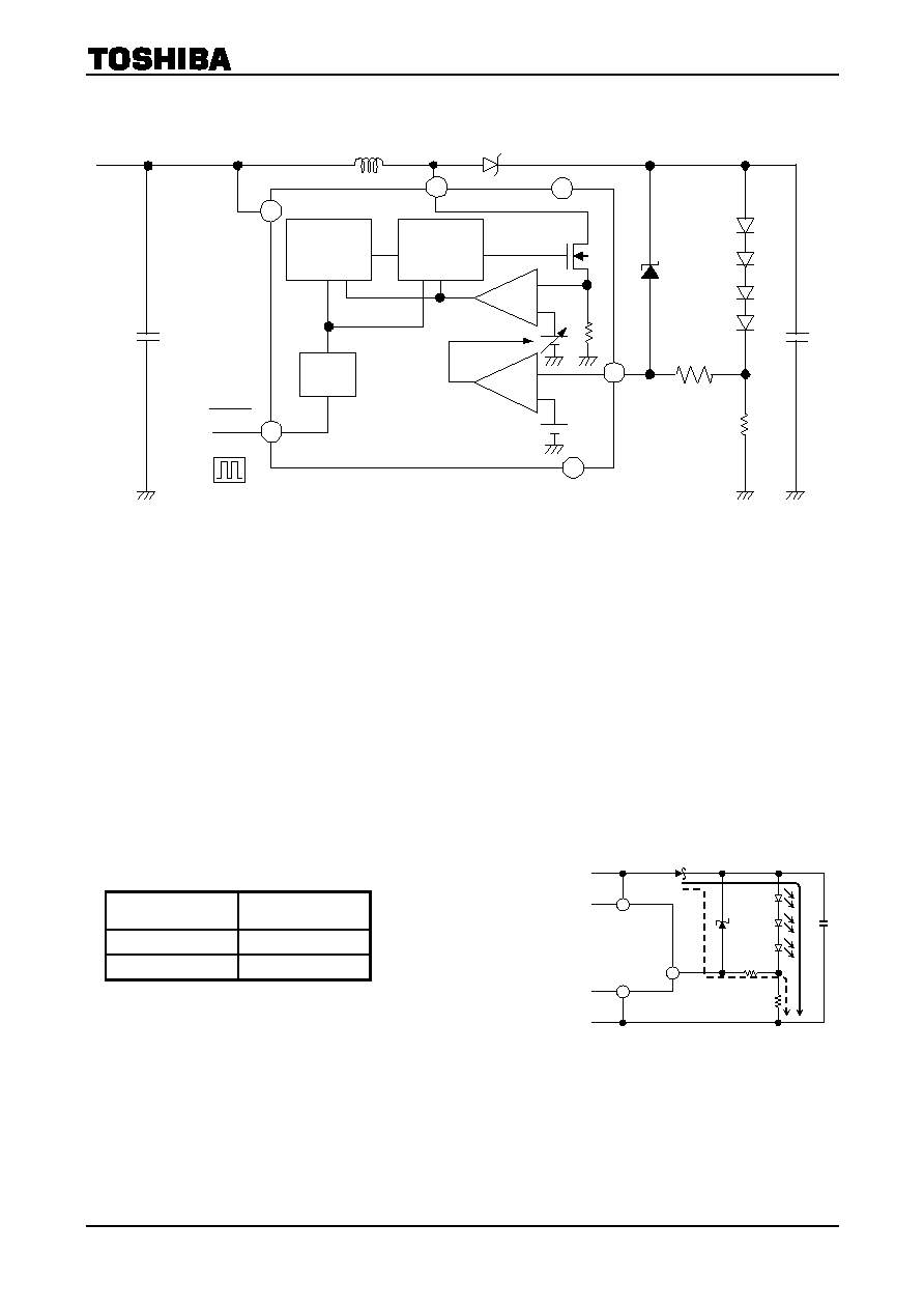
CTL
AMP.
Error
AMP.
SW
NC
GND
SHDN
VIN
1
3
4
2
6
5
Monostable
multivibrator
for
reference
Monostable
multivibrator
for
off time control
Circuit
on/off
FB
Block Diagram
Pin Assignment (top view)
Note 1:
The IC may break if mounted 180 degrees in reverse. Ensure the device is correctly orientated before assembley
.
Pin Functions
No. Symbol
Function
1
SHDN
Input pin for IC ON/OFF control and variable LED I
F
.
SHDN=H Operation ModeSHDN=L Shutdown Mode (IC shutdown)
PWM signal input for IF control (see p.5)
This pin must be set to a certain logic level, as unstable output could result if the pin is
left open.
2
NC
No Connection or Connected to GND. (Note 2)
3
VIN
Supply voltage pin. Supply voltage range : 2.8V to 5.5V
4
SW
DC-DC converter switching pin � switch incorporates N-ch MOSFET.
5
GND Ground
pin.
6
FB
Connected to the cathode of LED.
Note 2:
The NC terminal is not connected to the internal circuit.
SHDN
(NC)
VIN
FB
GND
SW
Q
1
2
3 4
5
6

TB62756FUG
2005-11-8
3
I/O Equivalent Pin Circuits
1. SHDN
pin
2. NC pin
3. SW
pin
4. FB pin
4
SW
VIN
6
FB
The NC pin is not connected to any internal circuit.
VIN
1
SHDN
2
NC
TB62756FUG
2005-11-8
4
PWM
VIN
4.7-10�H
1�F
2.2�F
16
@20mA
500
Vz=24V
CTL
AMP.
Error
AMP.
SW
NC
GND
SHDN
VIN
1
3
4
2
6
5
Monostable
multivibrator
for
reference
Monostable
multivibrator
for
off time control
Circuit
on/off
FB
Application Circuit Example
Protection at the time of LED opening
The zener diode in the application circuit example is necessary for the provision of over-voltage protection for
when the LED becomes open. As the IC does not incorporate a voltage protection circuit, it is strongly advised that
a zener diode be connected.
The zener diode should satisfy the following conditions:
i)
Less than maximum output voltage of 24V
ii) Greater than the total series LED V
F
iii) Less than the maximum output capacitance C
2
.
Moreover, by connecting a protection circuit such as R_ZD in the figure below, it is possible to control the output
current when the LED becomes open, and to use a zener diode of lower tolerance.
An example of IZD control by R_ZD connection. (RSENS
= 16 )
R_DZ (
) IZD
(mA)
500 0.6
(Typ.)
100 2.8
(Typ.)
In order to avoid adverse effects on driver characteristics,
Toshiba recommends a resistance of 500 ohms or less.
Protection circuit application
SW
GND FB
S-Di
IZD
1
�F
C2
R_ZD
RSENS
IF

TB62756FUG
2005-11-8
5
Output-side Capacitor Setting
It is recommended that the value of C2 be equal to, or greater than 1.0 (
�F).
External Inductor Size Setting
For each number of LEDs, the selected inductance should be greater than the value indicated in the
table below.
Number of LEDs
Inductance (Unit:
�H) Note
2 4.7
3
4
6.8
5
6
10
I
F
= 20 mA
Control of I
F
The resistance RSENS is connected between the FB pin and the GND pin.
The average current is controlled by the RSENS value, and calculated using the following equation:
I
F
(mA) = [ 325mV / RSENS() ]
Margin of error is �5%.
Dimming using PWM signal input
A dimming function can also by applied using a PWM signal.
[Notes]
When using a PWM signal, the minimum pulse width of the PWM should be greater than 33�s.
Duty ratio of PWM function should be set at 10% - 90%.
The recommended PWM frequency should be 100Hz - 10kHz.
<<Output current is calculated using the following equation>>
I
F
(mA) =
RSENS []
325[mV]
� ON Duty [%]

TB62756FUG
2005-11-8
6
Absolute Maximum Ratings
(T
a
=
25�C, unless otherwise specified)
Characteristics Symbol
Ratings Unit
Power supply voltage
V
IN
-0.3 to 6.0
V
Input voltage
V
SHDN
-0.3 to V
IN
+ 0.3(Note3)
V
Switching pin voltage
V
O (SW)
-0.3 to 24
V
Switching pin current
I
O (SW)
380 mA
0.41 (IC only)
Power Dissipation
P
D
0.47 (IC mounted on PCB)(Note4)
W
R
th (j-a) 1
300 (IC only)
Thermal resistance
R
th (j-a) 2
260 (IC mounted on PCB)
�C/W
Operating temperature range
T
opr
-40 to 85
�C
Storage temperature
T
stg
-55 to 150
�C
Maximum junction temperature
T
j
150
�C
Note3: However, do not exceed 6V.
Note4: Power dissipation is reduced by 3.8mW/�C from the maximum rating for every 1�C exceeding the ambient
temperature of 25�C (when the IC is mounted on a PCB).
Recommended Operating Condition
(T
a
=
-
40 to 85�C, unless otherwise specified)
Characteristics Symbol Test
Conditions Min.
Typ.
Max.
Unit
Power supply voltage
V
IN
2.8
5.5 V
SHDN pin input pulse width
tpw
ON/OFF duty width
33
�s
LED current (Average value)
I
F1
V
IN
= 3.6 V, R
SENS
= 16
4LEDs, T
a
= 25�C
20
A
Electrical Characteristics
(T
a
=
25�C V
IN
=
2.8~5.5 V, unless otherwise specified)
Characteristics Symbol Test
Conditions Min.
Typ.
Max.
Unit
Operating consumption current
I
IN (ON)
V
IN
= 6.0 V, R
SENS
= 16
0.9 1.5 mA
Standby consumption current
I
IN (OFF)
V
IN
= 3.6 V, V
SHDN
= 0 V
0.5 1.0 �A
SHDN pin H level input voltage
V
SHDN (H)
1.3
V
IN
V
SHDN pin L level input voltage
V
SHDN (L)
0
0.4 V
SHDN pin current
I
SHDN
V
IN
= 3.6 V, V
SHDN
= 3.6 V
-10 0 10 �A
Integrated MOS-FET switching
frequency
f
OSC
V
IN
= 3.6 V, V
SHDN
= 3.6 V
0.77
1.1
1.43
MHz
Switching pin protection voltage
V
O (SW)
25 V
Switching pin current
I
O (SW)
400 mA
Switching pin leakage current
I
OZ (SW)
0.5 1 �A
FB pin feedback voltage
V
FB
V
IN
= 3.6 V, R
SENS
= 16
L = 4.7
�H
308 325 342
mV
FB pin line regulation
V
FB
V
IN
= 3.6 V center
V
IN
= 3.0V to 5.0V
-5
5 %

TB62756FUG
2005-11-8
7
1. Application Circuit Example and Measurement Data (reference data)
Note: These application examples are provided for reference only. Thorough evaluation and testing should be
implemented when designing your application's mass production design.
S-Di
L
1
V
IN
=
2.8 to 5.5 V
C
1
=
2.2
�
F
C
2
=
1.0
�
F
RSENS
=
16
V
IN
SW
FB
GND
SHDN
WLEDs
2 to 6
�
Evaluation conditions (Ta
= 25�C)
L
1
: CXLD120 series (NEO MAX CO.,Ltd.)
(Size: 2.5 mm
� 3.0 mm � 1.2 mm)
C
1
: C2012JB1E225K (TDK Corp.)
C
2
: C2012JB1E105K (TDK Corp.)
S-Di
: CUS02 1 A/30 V (TOSHIBA Corp.)
WLEDs : NSCW215T (NICHIA Corp.)
RSENS : RK73B1ETBK (KOA Corp.)
Input Voltage - Efficiency/Output Current
4LED Drive, L=6.8�H
10
15
20
25
30
35
2.8
3.1
3.4
3.7
4
4.3
4.6
4.9
5.2
5.5
VIN(V)
IO
U
T
(
m
A
)
50
60
70
80
90
100
E
f
f
i
ci
e
n
cy(
%
)
IOUT
Efficiency
I F
(mA
)
IF
Efficiency
<Measurement Data>
Efficiency in the range of V
IN
= 2.8 to 5.5 V
Efficiency
(%)
Average Efficiency (%)
2 LEDs
82.60 to 88.46
86.29
3 LEDs
82.69 to 87.78
85.95
4 LEDs
80.73 to 86.22
83.05
5 LEDs
80.73 to 87.28
83.45
6 LEDs
79.78 to 85.55
81.15
Output current in the range of V
IN
= 3.0 to 5.0 V (V
IN
= 3.6 V typ.)
Tolerance (%)
Output Current (mA)
V
IN
= 3.6 V
Min Max
2 LEDs
21.13
-3.50 1.77
3 LEDs
20.60
-1.95 1.38
4 LEDs
20.87
-1.75 1.11
5 LEDs
20.06
-1.81 1.15
6 LEDs
19.90
-1.95 1.28
Input Voltage - Efficiency/Output Current
2LED Drive, L=4.7�H
10
15
20
25
30
35
2.8
3.1
3.4
3.7
4
4.3
4.6
4.9
5.2
5.5
VIN(V)
IO
U
T
(
m
A
)
50
60
70
80
90
100
E
f
f
i
ci
e
n
cy(
%
)
IOUT
Efficiency
I F
(mA
)
IF
Efficiency
Input Voltage - Efficiency/Output Current
3LED Drive, L=6.8�H
10
15
20
25
30
35
2.8
3.1
3.4
3.7
4
4.3
4.6
4.9
5.2
5.5
VIN(V)
IO
U
T
(
m
A
)
50
60
70
80
90
100
E
f
f
i
ci
e
n
cy(
%
)
IOUT
Efficiency
I F
(mA
)
IF
Efficiency
Input Voltage - Efficiency/Output Current
5LED Drive, L=10�H
10
15
20
25
30
35
2.8
3.1
3.4
3.7
4
4.3
4.6
4.9
5.2
5.5
VIN(V)
IO
U
T
(
m
A
)
50
60
70
80
90
100
E
f
f
i
ci
e
n
cy(
%
)
IOUT
Efficiency
I F
(mA
)
IF
Efficiency
Input Voltage - Efficiency/Output Current
6LED Drive, L=10�H
10
15
20
25
30
35
2.8
3.1
3.4
3.7
4
4.3
4.6
4.9
5.2
5.5
VIN(V)
IO
U
T
(
m
A
)
50
60
70
80
90
100
E
f
f
i
ci
e
n
cy(
%
)
IOUT
Efficiency
I F
(mA
)
IF
Efficiency

TB62756FUG
2005-11-8
8
2. Application Circuit Example and Measurement Data (reference data)
Note: These application examples are provided for reference only. Thorough evaluation and testing should be
implemented when designing your application's mass production design.
S-Di
L
1
V
IN
=
2.8 to 5.5 V
C
1
=
2.2
�
F
C
2
=
1.0
�
F
RSENS
=
16
V
IN
SW
FB
GND
SHDN
WLEDs
2 to 6
�
Evaluation conditions (Ta
= 25�C)
L
1
: 1001AS series (TOKO, INC)
(Size: 3.6 mm
� 3.6 mm � 1.2 mm)
C
1
: C2012JB1E225K (TDK Corp.)
C
2
: C2012JB1E105K (TDK Corp.)
S-Di
: CUS02 1 A/30 V (TOSHIBA Corp.)
WLEDs : NSCW215T (NICHIA Corp.)
RSENS : RK73B1ETBK (KOA Corp.)
Input Voltage - Efficiency/Output Current
2LED Drive, L=4.7�H
10
15
20
25
30
35
2.8
3.1
3.4
3.7
4
4.3
4.6
4.9
5.2
5.5
VIN(V)
IO
U
T
(
m
A
)
50
60
70
80
90
100
E
f
f
i
ci
e
n
cy(
%
)
IOUT
Efficiency
I F
(mA
)
IF
Efficiency
Input Voltage - Efficiency/Output Current
5LED Drive, L=10�H
10
15
20
25
30
35
2.8
3.1
3.4
3.7
4
4.3
4.6
4.9
5.2
5.5
VIN(V)
IO
U
T
(
m
A
)
50
60
70
80
90
100
E
f
f
i
ci
e
n
cy(
%
)
IOUT
Efficiency
I F
(mA
)
IF
Efficiency
Input Voltage - Efficiency/Output Current
3LED Drive, L=6.8�H
10
15
20
25
30
35
2.8
3.1
3.4
3.7
4
4.3
4.6
4.9
5.2
5.5
VIN(V)
IO
U
T
(
m
A
)
50
60
70
80
90
100
E
f
f
i
ci
e
n
cy(
%
)
IOUT
Efficiency
I F
(mA
)
IF
Efficiency
Input Voltage - Efficiency/Output Current
6LED Drive, L=10�H
10
15
20
25
30
35
2.8
3.1
3.4
3.7
4
4.3
4.6
4.9
5.2
5.5
VIN(V)
IO
U
T
(
m
A
)
50
60
70
80
90
100
E
f
f
i
ci
e
n
cy(
%
)
IOUT
Efficiency
I F
(mA
)
IF
Efficiency
Input Voltage - Efficiency/Output Current
4LED Drive, L=6.8�H
10
15
20
25
30
35
2.8
3.1
3.4
3.7
4
4.3
4.6
4.9
5.2
5.5
VIN(V)
IO
U
T
(
m
A
)
50
60
70
80
90
100
E
f
f
i
ci
e
n
cy(
%
)
IOUT
Efficiency
I F
(mA
)
IF
Efficiency
<Measurement Data>
Efficiency in the range of VIN = 2.8 to 5.5 V
Efficiency
(%)
Average Efficiency (%)
2 LEDs
83.10 to 88.60
86.55
3 LEDs
81.32 to 86.47
84.54
4 LEDs
79.15 to 84.63
81.30
5 LEDs
79.72 to 86.39
82.87
6 LEDs
78.91 to 85.10
80.47
Output current in the range of VIN = 3.0 to 5.0 V (V
IN
= 3.6 V typ.)
Tolerance (%)
Output Current (mA)
V
IN
= 3.6 V
Min Max
2 LEDs
21.17
-3.32 1.73
3 LEDs
20.85
-1.95 1.38
4 LEDs
20.56
-1.79 1.15
5 LEDs
20.10
-1.82 1.22
6 LEDs
19.95
-1.94 1.26

TB62756FUG
2005-11-8
9
3. Application Circuit Example and Measurement Data (reference data)
Note: These application examples are provided for reference only. Thorough evaluation and testing should be
implemented when designing your application's mass production design.
S-Di
L
1
V
IN
=
2.8 to 5.5 V
C
1
=
2.2
�
F
C
2
=
1.0
�
F
RSENS
=
16
V
IN
SW
FB
GND
SHDN
WLEDs
2 to 6
�
Evaluation conditions (Ta
= 25�C)
L
1
:
LQH2M
series
(Murata Manufacturing Co.,Ltd.)
(Size: 2.0 mm
� 1.6 mm � 0.95 mm)
C
1
: C2012JB1E105K (TDK Corp.)
C
2
: C2012JB1E105K (TDK Corp.)
S-Di
: CUS02 1 A/30 V (TOSHIBA Corp.)
WLEDs : NSCW215T (NICHIA Corp.)
RSENS : RK73B1ETBK (KOA Corp.)
Input Voltage - Efficiency/Output Current
2LED Drive, L=4.7�H
10
15
20
25
30
35
2.8
3.1
3.4
3.7
4
4.3
4.6
4.9
5.2
5.5
VIN(V)
IO
U
T
(
m
A
)
50
60
70
80
90
100
E
f
f
i
ci
e
n
cy(
%
)
IOUT
Efficiency
I F
(mA
)
IF
Efficiency
Input Voltage - Efficiency/Output Current
5LED Drive, L=10�H
10
15
20
25
30
35
2.8
3.1
3.4
3.7
4
4.3
4.6
4.9
5.2
5.5
VIN(V)
IO
U
T
(
m
A
)
50
60
70
80
90
100
E
f
f
i
ci
e
n
cy(
%
)
IOUT
Efficiency
I F
(mA
)
IF
Efficiency
Input Voltage - Efficiency/Output Current
3LED Drive, L=6.8�H
10
15
20
25
30
35
2.8
3.1
3.4
3.7
4
4.3
4.6
4.9
5.2
5.5
VIN(V)
IO
U
T
(
m
A
)
50
60
70
80
90
100
E
f
f
i
ci
e
n
cy(
%
)
IOUT
Efficiency
I F
(mA
)
IF
Efficiency
Input Voltage - Efficiency/Output Current
6LED Drive, L=10�H
10
15
20
25
30
35
2.8
3.1
3.4
3.7
4
4.3
4.6
4.9
5.2
5.5
VIN(V)
IO
U
T
(
m
A
)
50
60
70
80
90
100
E
f
f
i
ci
e
n
cy(
%
)
IOUT
Efficiency
I F
(mA
)
IF
Efficiency
Input Voltage - Efficiency/Output Current
4LED Drive, L=6.8�H
10
15
20
25
30
35
2.8
3.1
3.4
3.7
4
4.3
4.6
4.9
5.2
5.5
VIN(V)
IO
U
T
(
m
A
)
50
60
70
80
90
100
E
f
f
i
ci
e
n
cy(
%
)
IOUT
Efficiency
I F
(mA
)
IF
Efficiency
<Measurement Data>
Efficiency in the range of VIN = 2.8 to 5.5 V
Efficiency
(%)
Average Efficiency (%)
2 LEDs
82.37 to 88.70
86.38
3 LEDs
80.19 to 86.55
84.12
4 LEDs
78.11 to 84.54
80.16
5 LEDs
74.79 to 84.94
79.94
6 LEDs
74.14 to 83.47
77.17
Output current in the range of VIN = 3.0 to 5.0 V (V
IN
= 3.6 V typ.)
Tolerance (%)
Output Current (mA)
V
IN
= 3.6 V
Min Max
2 LEDs
21.19
-3.26 1.69
3 LEDs
20.90
-1.87 2.17
4 LEDs
20.63
-1.78 1.01
5 LEDs
20.09
-1.88 1.25
6 LEDs
19.93
-1.99 1.07

TB62756FUG
2005-11-8
10
4. Application Circuit Example and Measurement Data (reference data)
Note: These application examples are provided for reference only. Thorough evaluation and testing should be
implemented when designing your application's mass production design.
S-Di
L
1
V
IN
=
2.8 to 5.5 V
C
1
=
2.2
�
F
C
2
=
1.0
�
F
RSENS
=
16
V
IN
SW
FB
GND
SHDN
WLEDs
2 to 6
�
Evaluation conditions (Ta
= 25�C)
L
1
: VLF3010A series (TDK Corp.)
(Size: 3.0 mm
� 3.0 mm � 1.0 mm)
C
1
: C2012JB1E225K (TDK Corp.)
C
2
: C2012JB1E105K (TDK Corp.)
S-Di
: CUS02 1 A/30 V (TOSHIBA Corp.)
WLEDs : NSCW215T (NICHIA Corp.)
RSENS : RK73B1ETBK (KOA Corp.)
Input Voltage - Efficiency/Output Current
2LED Drive, L=4.7�H
10
15
20
25
30
35
2.8
3.1
3.4
3.7
4
4.3
4.6
4.9
5.2
5.5
VIN(V)
IO
U
T
(
m
A
)
50
60
70
80
90
100
E
f
f
i
ci
e
n
cy(
%
)
IOUT
Efficiency
I F
(mA
)
IF
Efficiency
Input Voltage - Efficiency/Output Current
5LED Drive, L=10�H
10
15
20
25
30
35
2.8
3.1
3.4
3.7
4
4.3
4.6
4.9
5.2
5.5
VIN(V)
IO
U
T
(
m
A
)
50
60
70
80
90
100
E
f
f
i
ci
e
n
cy(
%
)
IOUT
Efficiency
I F
(mA
)
IF
Efficiency
Input Voltage - Efficiency/Output Current
3LED Drive, L=6.8�H
10
15
20
25
30
35
2.8
3.1
3.4
3.7
4
4.3
4.6
4.9
5.2
5.5
VIN(V)
IO
U
T
(
m
A
)
50
60
70
80
90
100
E
f
f
i
ci
e
n
cy(
%
)
IOUT
Efficiency
I F
(mA
)
IF
Efficiency
Input Voltage - Efficiency/Output Current
6LED Drive, L=10�H
10
15
20
25
30
35
2.8
3.1
3.4
3.7
4
4.3
4.6
4.9
5.2
5.5
VIN(V)
IO
U
T
(
m
A
)
50
60
70
80
90
100
E
f
f
i
ci
e
n
cy(
%
)
IOUT
Efficiency
I F
(mA
)
IF
Efficiency
Input Voltage - Efficiency/Output Current
4LED Drive, L=6.8�H
10
15
20
25
30
35
2.8
3.1
3.4
3.7
4
4.3
4.6
4.9
5.2
5.5
VIN(V)
IO
U
T
(
m
A
)
50
60
70
80
90
100
E
f
f
i
ci
e
n
cy(
%
)
IOUT
Efficiency
I F
(mA
)
IF
Efficiency
<Measurement Data>
Efficiency in the range of VIN = 2.8 to 5.5 V
Efficiency
(%)
Average Efficiency (%)
2 LEDs
79.85 to 86.97
84.02
3 LEDs
80.19 to 85.32
83.39
4 LEDs
78.77 to 83.60
80.69
5 LEDs
79.72 to 86.39
82.87
6 LEDs
78.91 to 85.10
80.49
Output current in the range of VIN = 3.0 to 5.0 V (V
IN
= 3.6 V typ.)
Tolerance (%)
Output Current (mA)
V
IN
= 3.6 V
Min Max
2 LEDs
21.19
-3.08 1.67
3 LEDs
20.89
-1.86 1.33
4 LEDs
20.64
-1.68 1.11
5 LEDs
20.10
-1.82 1.22
6 LEDs
19.95
-1.94 1.26

TB62756FUG
2005-11-8
11
5. Application Circuit Example and Measurement Data (reference data)
Note: These application examples are provided for reference only. Thorough evaluation and testing should be
implemented when designing your application's mass production design.
S-Di
L
1
V
IN
=
2.8 to 5.5 V
C
1
=
2.2
�
F
C
2
=
1.0
�
F
RSENS
=
16
V
IN
SW
FB
GND
SHDN
WLEDs
2 to 4
�
Evaluation conditions (Ta
= 25�C)
L
1
: 32R51 (KOA Corp.)
(Size: 3.2 mm
� 2.5 mm � 0.6 mm)
C
1
: C2012JB1E225K (TDK Corp.)
C
2
: C2012JB1E105K (TDK Corp.)
S-Di
: CUS02 1 A/30 V (TOSHIBA Corp.)
WLEDs : NSCW215T (NICHIA Corp.)
RSENS : RK73B1ETBK (KOA Corp.)
Input Voltage - Efficiency/Output Current
3LED Drive, L=5.1H
10
15
20
25
30
35
2.8
3.1
3.4
3.7
4
4.3
4.6
4.9
5.2
5.5
VIN(V)
O
u
t
p
ut
C
urre
nt
(
m
A
)
50
60
70
80
90
100
Ef
f
i
ci
ency
(
%
)
Iout
Efficiency
I F
(mA
)
IF
Efficiency
Input Voltage - Efficiency/Output Current
4LED Drive, L=5.1H
10
15
20
25
30
35
2.8
3.1
3.4
3.7
4
4.3
4.6
4.9
5.2
5.5
VIN(V)
O
u
t
p
ut
C
u
rrent
(
m
A
)
50
60
70
80
90
100
E
f
f
i
ci
enc
y
(
%)
Iout
Efficiency
I F
(mA
)
IF
Efficiency
<Measurement Data>
Efficiency in the range of VIN = 2.8 to 5.5 V
Efficiency
(%)
Average Efficiency (%)
2 LEDs
83.08 to 89.23
86.73
3 LEDs
79.02 to 86.30
83.52
4 LEDs
75.75 to 83.83
80.78
Output current in the range of VIN = 3.0 to 5.0 V (V
IN
= 3.6 V typ.)
Tolerance (%)
Output Current (mA)
V
IN
= 3.6 V
Min Max
2 LEDs
21.06
-2.46 4.02
3 LEDs
20.57
-2.39 2.94
4 LEDs
20.22
-2.28 2.65
Input Voltage - Efficiency/Output Current
2LED Drive, L=5.1H
10
15
20
25
30
35
2.8
3.1
3.4
3.7
4
4.3
4.6
4.9
5.2
5.5
VIN(V)
O
u
t
p
ut
C
urrent
(
m
A
)
50
60
70
80
90
100
E
f
fi
c
i
e
n
c
y
(%
)
Iout
Efficiency
I F
(mA
)
IF
Efficiency

TB62756FUG
2005-11-8
12
Package Dimensions
Weight: 0.016 g (typ.)

TB62756FUG
2005-11-8
13
Notes on Contents
Block Diagrams
Some functional blocks, circuits, or constants may be omitted or simplified in the block diagram for
explanatory purposes.
Equivalent Circuitry
Some parts of the equivalent circuitry may have been omitted or simplified for explanatory purposes.
Maximum Ratings
The absolute maximum ratings of a semiconductor device are a set of specified parameter values that
must not be exceeded during operation, even for an instant.
If any of these ratings are exceeded during operation, the electrical characteristics of the device may be
irreparably altered and the reliability and lifetime of the device can no longer be guaranteed.
Moreover, any exceeding of the ratings during operation may cause breakdown, damage and/or
degradation in other equipment. Applications using the device should be designed so that no maximum
rating will ever be exceeded under any operating conditions.
Before using, creating and/or producing designs, refer to and comply with the precautions and conditions
set forth in this document.
Application Examples
The application examples provided in this data sheet are provided for reference only. Thorough
evaluation and testing should be implemented when designing your application's mass production design.
In providing these application examples, Toshiba does not grant the use of any industrial property rights.
Handling of the IC
Ensure that the product is installed correctly to prevent breakdown, damage and/or degradation in the
product or equipment.
Short circuiting between output and line to ground faults may result in damage to the IC. Please exercise
precaution in designing the output line, power line and GND line so as to prevent such damage.
Be careful to insert the IC correctly. Inserting the IC the wrong way (e.g., wrong direction) may result in
damage to the IC.
Please exercise precaution in handling external components as shorting and opening such components may
cause an overcurrent, which in turn may result in power overcurrent and/or in damage to the IC.
Overcurrent and Thermal Protection
Toshiba does not guarantee that these protection functions will prevent damage to the product. These
functions are only intended as a temporary means of preventing output short circuiting and other
abnormal conditions.
If the guaranteed operating ranges of this product are exceeded, these protection functions may not
function as intended and this product might be damaged due to output short circuiting.
The overcurrent protection function is intended to protect this product from temporary short circuiting only.
Short circuiting that last for a long time may cause excessive stress and damage to this product.

TB62756FUG
2005-11-8
14