 | –≠–ª–µ–∫—Ç—Ä–æ–Ω–Ω—ã–π –∫–æ–º–ø–æ–Ω–µ–Ω—Ç: GT-64010A | –°–∫–∞—á–∞—Ç—å:  PDF PDF  ZIP ZIP |
W e b : w w w . g a l il e o T .c o m E m a i l: i n fo @ g a l i le o T . co m T el : ( 40 8 ) 4 51 - 1 4 00 F a x: ( 4 08 ) 4 5 1- 1 4 0 4
System Controller with
PCI Interface for R4XXX/
R5000 Family CPUs
GT-64010A
Preliminary
Revision 1.1
December 1996
FEATURES
NOTE: Always contact Galileo Technology for
possible updates before starting a design.
Galileo
Technology
TM
∑
Integrated system controller with PCI bus interface for
high performance embedded controller applications
∑
Supports the R4600/4650/4700/R5000 CPUs
∑
Up to 50MHz CPU bus frequency
∑
64 byte write buffer
- 64-bit wide
- 8 levels deep
∑
256KB or 512KB zero-wait-state secondary cache
support by using GT-64012 (R4600/R4700)
∑
DRAM controller
- Page mode and EDO DRAMs
- 512MB address space
- 256KB-16MB device depth
- 1- 4 banks supported directly
- 32-bit or 64-bit data width
- Different size for each bank
∑
Device controller
- 5 chip selects
- Programmable timing for each chip select
- Supports several types of standard memories
(ROM / Flash / SRAM) and I/O controllers
- Up to 160MB address space
- External wait support
- 8-,16-,32- and 64-bit width device (and boot) sup-
port
∑
External parity support for user selected banks of
DRAM and devices
∑
DMA controller
- Four independent channels
- Chaining via linked lists of records
- Byte alignment on source and destination
- Transfers through a 32-byte internal FIFO
- Moves data between PCI, memory, and devices
∑
PCI bus
- Fully compatible with PCI 2.1 Specification
- High performance PCI interfaces via 96-bytes of
posted write and read prefetch buffers
- 32-bit PCI master and slave operations
- Provides clock speed of up to 33MHz with no wait
states on PCI (asynchronous from CPU bus)
- Supports burst operations on PCI for efficient data
transfer
- Supports doorbells between Host and PCI
- Supports flexible byte swapping - no need for CPU
intervention.
- Synchronization Barrier support from CPU to PCI
and from PCI to CPU.
∑
Host to PCI bridge
- Translates CPU cycles into PCI I/O or Memory
cycles
- Generates configuration Interrupt Acknowledge
and Special cycles on PCI
∑
PCI to Main Memory bridge
- Supports fast back-to-back transactions
- Flexible address mapping of both DRAM and
devices from PCI side
- Supports memory and I/O transactions to internal
configuration registers
- Supports locked operations
∑
PCI configuration registers are accessed from both
CPU and PCI side
∑
Three 24-bit wide and one 32-bit wide timers/counters
∑
5V Operation (3.3V operation using inexpensive sup-
port components
∑
256 PQFP or 272 Ball-BGA
R4xxx CPU
DRAM
Flash
GT-64010A
SCSI
Network
PCI Bus
Other
SysAD Bus
Address
&
Control
Data
Data
BYPASS
32
32
64
I/O

GT-64010A System Controller with PCI Interface for R4XXX/R5000 Family CPUs
2
R e v i s i o n 1 . 1
Galileo
Technology
T M
1. OVERVIEW
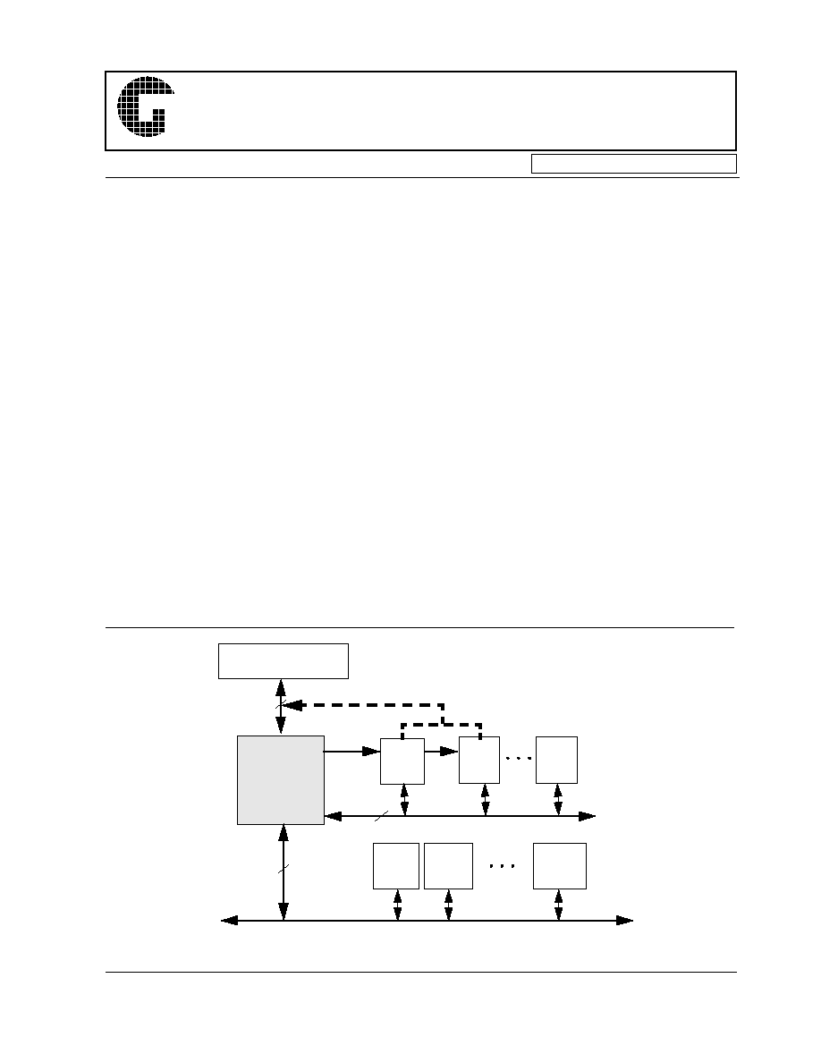
The GT-64010A is a highly integrated system controller that supports middle to high performance embedded control
applications with state-of-the-art 64-bit MIPS processors, while significantly reducing their cost, complexity, device
count, and board space.
The architecture of the chip supports several optional system architectures for different applications and cost/perfor-
mance points. It is possible to design a powerful system with minimal glue logic, or add commodity logic (controlled by
the GT-64010A) for differentiated system architectures that attain higher performance.
The GT-64010A has a three bus architecture:
a)
64-bit interface to the CPU,
b)
32-bit interface to the memory subsystem, with a bypassing option to create a 64-bit path to the CPU,
c)
32-bit interface to the PCI bus.
The three buses are de-coupled from each other in most accesses, enabling concurrent operation of the CPU, PCI
devices, and accesses to memory. For example, the CPU can write to the on-chip write buffer, a DMA agent can move
data from DRAM to its own buffers, and a PCI device can write into an on-chip FIFO at the same time.
1.1
Processor Interface
The GT-64010A supports without glue logic the IDT/MIPS family of R4xxx and R5000 Orion processors. It supports
bus frequencies of up to 50MHz, while the processor can operate internally at 80 to 200MHz. The GT-64010A has a
deep write buffer with the ability to absorb several write transactions from the CPU. For systems that want to increase
performance even more, the GT-64010A supports the Galileo GT-64012 secondary cache controller. Systems with
CPUs that run internally at 3x or more of the external frequency can particularly benefit from this option.
1.2
DRAM and Device Interface
The GT-64010A has a flexible DRAM controller. It supports EDO (Hyperpage) as well as standard page mode DRAMs.
With 60ns standard DRAMs, the GT-64010A can return data at
7-2-2-2 to the CPU (four wait states to the first access).
The DRAM controller supports different depth devices in each bank for base configuration at manufacturing, and allow-
ing for field upgrades by end users. It supports 32-bit wide DRAMs for high granularity in applications where small
memory size is desirable, or 64-bit wide DRAM where higher memory performance is needed.
The GT-64010A memory controller supports different types of memory and I/O devices. It has the control signals and
the timing programmability to support devices like Flash, EPROMs, SRAMs, FIFOs, and I/O controllers, from 8-bit to
64-bit width.
Parity generation and checking is supported externally and is optional for each bank of DRAM or any other device on
the memory bus.
1.3
PCI Interface
The GT-64010A interfaces directly with the PCI bus. It can be either a master initiating a PCI bus operation or a target
responding to a PCI bus operation.
The GT-64010A incorporates 96-bytes of posted write and read prefetch buffers for efficient data transfer between the
CPU/DMA to PCI and PCI to main memory.
The GT-64010A becomes a PCI bus master when the CPU or the internal DMA engine initiates a bus cycle to a PCI
device. It translates the CPU cycle into the appropriate PCI bus cycle. These cycles can be either Memory, Interrupt
Acknowledge, Special, I/O, or Configuration cycles.
The GT-64010A acts as a target when a PCI device initiates a memory access (or an I/O access in the case of internal
registers). It responds to all memory read/write accesses, as well as to all configuration and I/O cycles in the case of
internal registers.
The GT-64010A contains the required PCI configuration registers. All the internal registers, including the PCI configu-
GT-64010A System Controller with PCI Interface for R4XXX/R5000 Family CPUs
3
R e v is io n 1 . 1
Galileo
Technology
TM
ration registers, can be accessed from both the CPU and the PCI.
The GT-64010A can also act as a PCI to Memory bridge, even without the presence of the CPU.
1.4
DMA Engines
The GT-64010A incorporates four high performance DMA engines. Each DMA engine has the capability to transfer
data between PCI devices and main memory or between devices residing on the 32-/64-bit memory bus. The DMA
uses an internal 32-byte FIFO for temporary storage of DMA data. Source and destination addresses can be non-
aligned on any byte address boundary. The DMA channels can be programmed by the CPU or by PCI masters, or with-
out CPU intervention via a linked list of records that is loaded by the DMA controller into the channel's working set
when a DMA transaction ends. The DMA supports increment/decrement/hold on source and destination addresses
independently.
2.
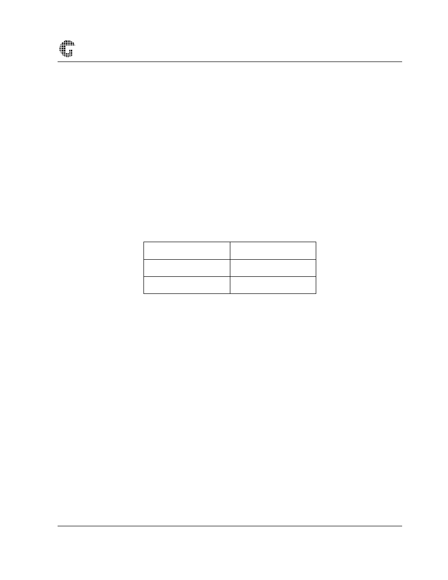
ORDERING INFORMATION
Please use the part numbers in the table below when placing orders for GT-64010 devices.
Package Type
Part Number
256 Pin PQFP
GT-64010A-P
272 Pin BGA
GT-64010A-B
GT-64010A System Controller with PCI Interface for R4XXX/R5000 Family CPUs
4
R e v i s i o n 1 . 1
Galileo
Technology
T M
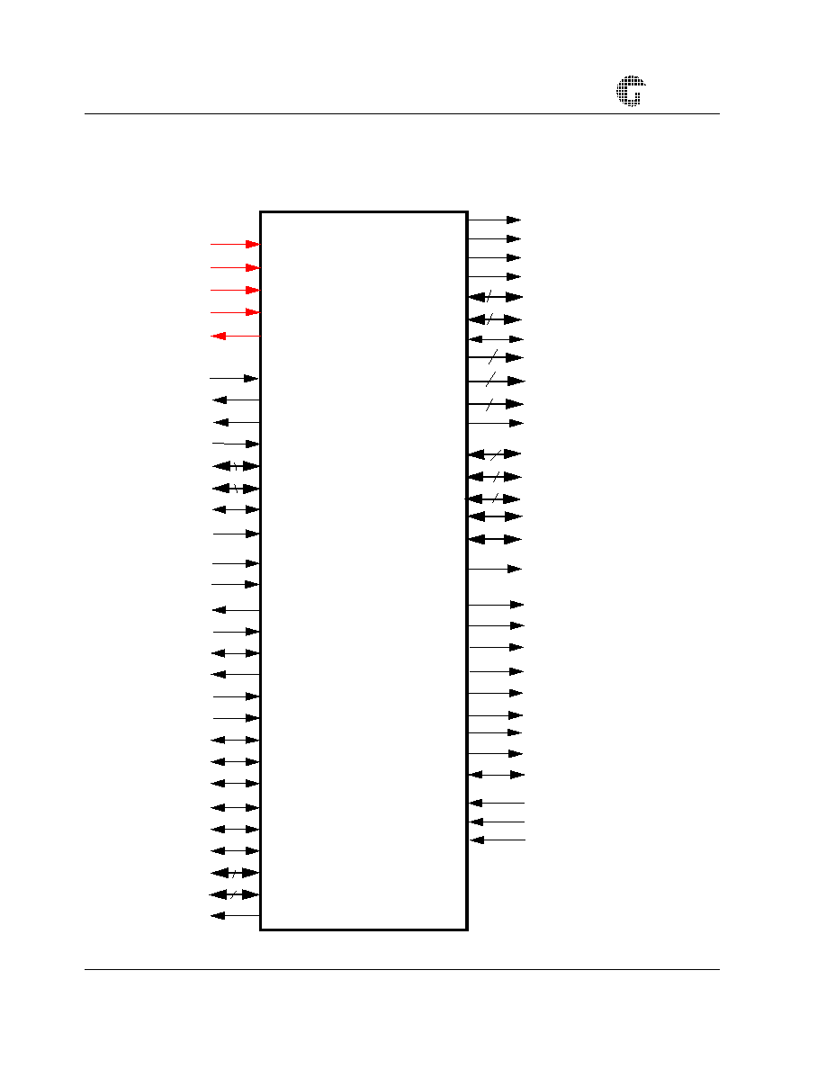
3. PIN INFORMATION
3.1 Logic
Symbol
ValidOut*
ValidIn*
WrRdy*
Release*
SysAD
SysCmd[8:0]
[63:0]
TClk
Interrupt*
Rst*
PClk
Req*
Gnt*
PErr*
SErr*
Lock*
DevSel*
Stop*
Frame*
Par
TRdy*
IRdy*
PAD[31:0]
CBE[3:0]*
DWr*
RAS[3:0]*
AD[31:28]/CS[3:0]*
OEO*
OEE*
OEB
ALE
OE64*
IdSel
ECAS[3:0]*
OCAS[3:0]*
LEO
DRAM
DMA
PCI
Interface
CPU
Interface
32
4
64
9
Int*
DAdr[6:4]/EWr[3:1]*
DAdr[10:7]/OWr[3:0]*
AD[27:24]/DMAAck[3:0]*
4
22
CSTiming*
LEE
LEAdrO
Hit/DMAReq[3]*
DMAReq[1]*/ParErr*
3
4
4
4
DAdr[11]/ADS*
AD[23:2]
Local
Address
& Data
Bus
Latch
Control
GT-64010A
AD[0]/BootCS*
AD[1]/ DevRW*
LEAdrE/DMAReq[2]*
DAdr[0]/BAdr[0]
4
4
&
Devices
DMAReq[0]*/Ready*
DAdr[1]/BAdr[1]
DAdr[2]/BAdr[2]
DAdr[3]/EWr[0]
JTRST*
JTMS
JTCLK
JTDI
JTDO
JTAG

GT-64010A System Controller with PCI Interface for R4XXX/R5000 Family CPUs
5
R e v is io n 1 . 1
Galileo
Technology
TM
3.2. Pin Assignment Table
Pin Name
Type
Description
CPU Interface
Release*
I
Release Interface: Signals to the GT-64010A that the processor is
releasing the system interface to slave state.
WrRdy*
O
Write Ready: The GT-64010A signals that it can accept a proces-
sor write request.
ValidIn*
O
Valid Input: The GT-64010A signals that it is driving valid data on
the SysAD bus, and a valid data identifier on the SysCmd bus.
ValidOut*
I
Valid Output: Signals that the processor is driving valid address or
data on the SysAD bus and a valid command or data identifier on
the SysCmd bus.
SysAD[63:0]
I/O
System Address/Data Bus: A 64-bit address and data bus for
communication between the processor and GT-64010A.
SysCmd[8:0]
I/O
System Command/Data Identifier Bus: A 9-bit bus for command
and data identifier transmission between the processor and GT-
64010A.
Interrupt*
I/O
Interrupt: An "OR" of all the internal interrupt sources on the GT-
64010A. This pin is also sampled as an input at reset for configura-
tion purposes.
TClk
I
Clock: The input clock to the GT-64010A (up to 50MHz).
PCI Interface
PClk
I
PCI Clock: It provides the timing for the PCI-related bus transac-
tion. The PCI clock range is between 0 and 33MHz.
Rst*
I
Reset: Resets the GT-64010A to its initial state. This signal must be
asserted for at least 10 PCI clock cycles. When in the reset state, all
PCI output pins are put into tristate and all open drain signals are
floated.
PAD[31:0]
I/O
Address/Data: 32-bit multiplexed PCI address and data lines. Dur-
ing the first clock of the transaction, PAD[31:0] contains a physical
byte address (32 bits). During subsequent clock cycles, PAD[31:0]
contains data.
CBE[3:0]*
I/O
Bus Command/Byte Enable: These are multiplexed on the same
PCI pins. During the address phase of the transaction, CBE[3:0]*
provide the bus command. During the data phase, these lines pro-
vide the byte enable. Byte enable determines which bytes carry
valid data.
Par
I/O
Parity: Calculated by the GT-64010A as an even parity bit for the
PAD[31:0] and CBE[3:0]* lines.
Frame*
I/O
Frame: It is asserted by the GT-64010A to indicate the beginning
and duration of a master transaction. Frame* asserts to indicate the
beginning of the cycle. While Frame* is asserted, data transfer con-
tinues. Frame* deasserts to indicate that the next data phase is the
final data phase transaction. Frame* is monitored by the GT-
64010A when it acts as a target.