
DA8444A.005
May 31, 1996
1
Reference
Voltage
Generator
6-BIT DAC
6-BIT DAC
6-BIT DAC
6-BIT DAC
6-BIT DAC
6-BIT DAC
6-BIT DAC
DAC7
6-BIT DAC
DAC6
DAC5
DAC4
DAC3
DAC2
DAC1
DAC0
VDD
A0 5
SDA 3
SCL 4
A1 6
A2 7
Vmax 2
GND
I C Bus
Slave
Receiver
2
1
8
MAS8444A
OCTAL 6-BIT TRIMMER IC
� Eight discrete DACs
� I
2
C-bus slave receiver
� Voltage output
DESCRIPTION
The MAS8444a comprises eight digital to analog
converters (DACs) each controlled by a two-wire I
2
C
bus. The DACs are individually programmed using an
6-bit word to select an output from one of 64 voltage
steps. The maximum output voltage of all DACs is set
by Vmax. At power-on all outputs are set to their lowest
value. The I
2
C-bus slave receiver has 3 programmable
address pins (2 in the SO16 package).
FEATURES
� Rail to rail output stages
� Octal 6-bit DACs on a single monolithic chip
� Power supply range from +5V to +12V
� -25
C to +85
�
C temperature range
� 16-pin PDIL and SO package
� pin to pin compatibility with TDA8444
APPLICATION
� Trimmer replacement
� Automatic gain control
� High resolution monitors
BLOCK DIAGRAM
DA8444A.005
May 31, 1996
2
1
2
3
4
5
6
7
8
SO16
9
10
11
12
13
14
15
16 DAC7
DAC6
DAC5
DAC4
DAC3
DAC2
DAC1
DAC0
VDD
Vmax
SDA
SCL
NC
A0
A1
GND
PDIP 16
VDD
Vmax
SDA
SCL
A0
A1
A2
GND
1
2
3
4
5
6
7
8
9
10
11
12
13
14
15
16 DAC7
DAC6
DAC5
DAC4
DAC3
DAC2
DAC1
DAC0
MAS8444AN
MAS8444AS
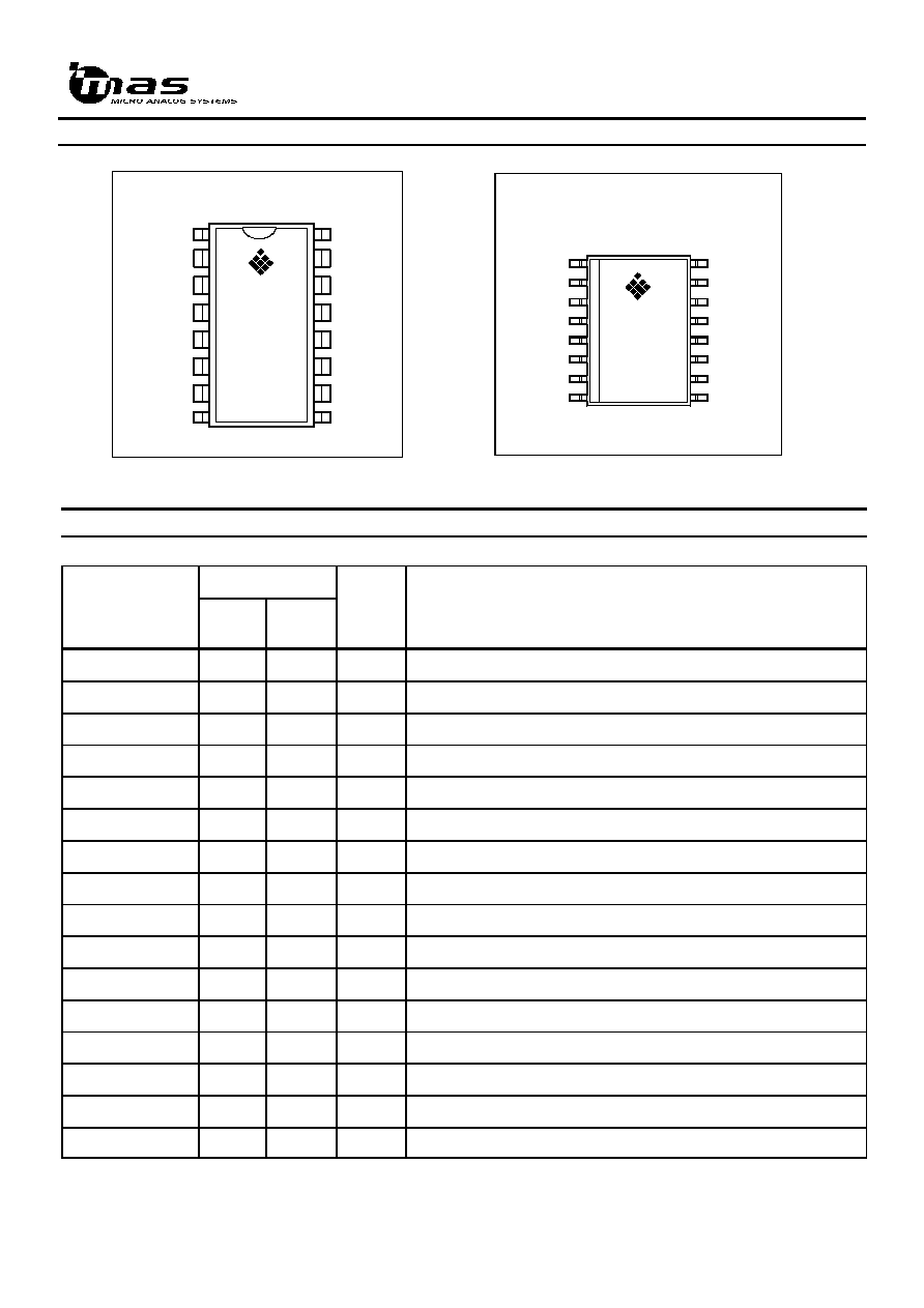
PIN CONFIGURATION
PIN DESCRIPTION
Pin name
Pin no.
I/O
Function
PDIP1
6
SO16
VDD
1
1
P
Positive supply voltage
Vmax
2
2
I
Control input for DAC maximum output voltage
SDA
3
3
I/O
I
2
C bus serial data input/output
SCL
4
4
I
I
2
C bus serial data clock
A
0
5
6
I
Programmable address bits for I
2
C bus slave receiver
A
1
6
7
I
Programmable address bits for I
2
C bus slave receiver
A
2
7
NC
I
Programmable address bits for I
2
C bus slave receiver
GND
8
8
G
Ground
DAC0
9
9
O
Analog voltage output
DAC1
10
10
O
Analog voltage output
DAC2
11
11
O
Analog voltage output
DAC3
12
12
O
Analog voltage output
DAC4
13
13
O
Analog voltage output
DAC5
14
14
O
Analog voltage output
DAC6
15
15
O
Analog voltage output
DAC7
16
16
O
Analog voltage output
DA8444A.005
May 31, 1996
3
ABSOLUTE MAXIMUM RATINGS
(conditions)
Parameter
Symbol
Conditions
Min
Max
Unit
Supply Voltage
VDD
-0.5
18
V
Supply current
IDD
-10
40
���
I
2
C-bus line voltage
V(3),V(4)
-0.5
5.9
V
Input voltage
Vin
-0.5
VDD+0.5
V
Output voltage
Vo
-0.5
VDD+0.5
�
Maximum current on any pin
(except pins 1 and 8)
Imax
10
mA
Total power dissipation
Ptot
500
mW
Operating ambient temperature
range
Tamb
-20
+70
o
C
Storage temperature range
Tstg
-65
+150
o
C
���������� �!#"
$��$��"
!#"
$ %
&
')(
(10324(
5
687893@A64B
9ACED
5
FGB
93@3H398IP545
2GQAR)SUTWVX64YG`Gacb
d8e
o
C
fWgUh)hpirqWs3gt8u8v
w3xyxA
3w4
E
xwx33w8
w33
Parameter
Symbol
Conditions
Min
Typ
Max
Unit
Supply Voltage
VDD
4.5
12
13.2
V
Supply current
IDD
No loads
6.0
10.0
17.0
mA
Voltage level from power
V1
1
4
V
Total power dissipation
Ptot
No loads, Vmax=VDD
120
mW
ELECTRICAL CHARACTERISTICS
Inputs
SDA, SCL input (pins 3, 4)
(All voltages are with respect to GND; Tamb = 25
o
C; VDD = 12V unless otherwise specified)
Parameter
Symbol
Conditions
Min
Typ
Max
Unit
Input voltage range
V
I
0
5.5
V
Input low voltage
V
IL
1.0
V
Input high voltage
V
IH
3.0
V
Input current low
I
IL
V(3),V(4) = -0.3V
-10
�A
Input current high
V
IH
V(3),V(4) = 6.0V
+10
�A

DA8444A.005
May 31, 1996
4
ELECTRICAL CHARACTERISTICS
Address Input (pins 5, 6, 7)
(All voltages are with respect to GND; Tamb = 25
o
C; VDD = 12V unless otherwise specified)
Parameter
Symbol
Conditions
Min
Typ
Max
Unit
Input voltage range
V
I
0
VDD
V
Input low voltage
V
IL
1.0
V
Input high voltage
V
IH
2.2
V
Input current low
I
IL
-7
-10
�A
Input current high
I
IH
1
�A
(All voltages are with respect to GND; Tamb = 25
o
C; VDD = 12V unless otherwise specified)
Parameter
Symbol
Conditions
Min
Typ
Max
Unit
Input current
I
2
7
10
�A
Effective voltage range
Vmax
1.0
VDD-2.0
V
DAC Outputs (pin 9 to 16)
(All voltages are with respect to GND; Tamb = 25
o
C; VDD = 12V unless otherwise specified)
Parameter
Symbol
Conditions
Min
Typ
Max
Unit
Output voltage range
Vo
0.1
VDD-0.5
V
Minimum output voltage
Vomin
data = 00; Io = +2mA
0.1
0.4
0.5
V
Max output voltage
Vomax
data = 3f; Io = -2mA; Vmax =
10
11.1
11.5
V
data = 3f; Io = -2mA;
see note 1
Temperature coefficient
Tc
1
mV/K
Gain error
data = 3F
2
%
Output impedance
Zo
data = 1F; -2mA < Io < +2mA
50
Output capacitive load
Co
2
nF
note 1: Vomax = Vmax + Vo(00)
SDA Output (pin 3)
(All voltages are with respect to GND; Tamb = 25
o
C; VDD = 12V unless otherwise specified)
Parameter
Symbol
Conditions
Min
Typ
Max
Unit
Output voltage low
V
OL
I
3
= 3.0 mA
0.2
0.4
V
Sink current
Isink
3
8
mA

DA8444A.005
May 31, 1996
5
SDA
SCL
Bit Transfer on the I C-bus
2
Data line
stable
(data valid)
Change
of data
allowed
S
P
1-7
8
9
1-7
8
9
1-7
8
9
Start
condition
Stop
condition
SDA
SCL
Address
Data
Data
R/W
Ack
Ack
Ack
Complete Data Transfer
ELECTRICAL CHARACTERISTICS
CONT.
Linearity
(All voltages are with respect to GND; Tamb = 25
o
C; VDD = 12V unless otherwise specified)
Parameter
Symbol
Conditions
Min
Typ
Max
Unit
Differential nonlinearity
DNL
Io = -2mA; Vmax = VDD
-0.5
0.1
0.5
LSB
Integral nonlinearity
INL
Io = -2mA; Vmax = VDD
-0.5
0.1
0.5
LSB
FUNCTIONS
I
2
C - bus
The MAS8444A I
2
C-bus interface is a receiver-only slave. Data is accepted from the I
2
C-bus in the following format.
S
0 1 0 0 A2 A1 A0 0
A
I3 I2 I1 I0 SD SC SB SA
A
D7 D6 D5 D4 D3 D2 D1 D0
A
P
Address byte
Instruction byte
First data byte
S
Start condition
A2, A1, A0
programmable address bits
P
Stop condition
I3, I2, I1, I0
instruction bits
A
Acknowledgement
SD, SC, SB, SA
sub-address bits
D7, D6, D5, D4, D3, D2, D2, D1, D0
data bits
I
2
C - bus
timing