 | –≠–ª–µ–∫—Ç—Ä–æ–Ω–Ω—ã–π –∫–æ–º–ø–æ–Ω–µ–Ω—Ç: MAS9078B1 | –°–∫–∞—á–∞—Ç—å:  PDF PDF  ZIP ZIP |
DA9078.002
17 April 2003
1 (10)
MAS9078
AM Receiver IC
∑
High Sensitivity
∑
Very Low Power Consumption
∑
Wide Supply Voltage Range
∑
Power Down Control
∑
Control for AGC On
∑
High Selectivity by Crystal Filter
∑
Fast Startup Feature
DESCRIPTION
The MAS9078 AM-Receiver chip is a highly sensitive,
simple to use AM receiver specially intended to
receive time signals in the frequency range from 40
kHz to 100 kHz. Only a few external components are
required for time signal receiver. The circuit has
preamplifier, wide range automatic gain control,
demodulator and output comparator built in. The
output signal can be processed directly by an
additional digital circuitry to extract the data from the
received signal. The control for AGC (automatic gain
control) can be used to switch AGC on or off if
necessary. Unlike MAS1016A and MAS1016B,
MAS9078 does not require AGC control procedure in
WWVB and JJY systems.
FEATURES
APPLICATIONS
∑
Highly Sensitive AM Receiver, 0.4
µ
V
RMS
typ.
∑
Wide Supply Voltage Range from 1.1 V to 3.6 V
∑
Very Low Power Consumption
∑
Power Down Control
∑
Fast
Startup
∑
Only a Few External Components Necessary
∑
Control for AGC On
∑
Wide Frequency Range from 40 kHz to 100 kHz
∑
High Selectivity by Quartz Crystal Filter
∑
Die and TSSOP-16 Package
∑
Time Signal Receiver WWVB (USA), JJY (Japan),
DCF77 (Germany) and MSF (UK)
∑
Receiver for ASK Modulated Data Signals
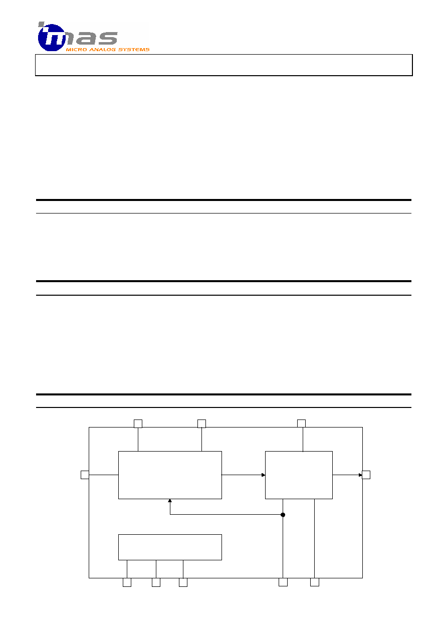
BLOCK DIAGRAM
AGC Amplifier
Demodulator
&
Comparator
Power Supply/Biasing
RFI
OUT
QI
QO
PDN
VDD
VSS
AGC
DEC
AON (=AGC on)

DA9078.002
17 April 2003
2 (10)
PAD LAYOUT
DIE size = 1.70 x 1.78 mm; PAD size = 100 x 100
µ
m
Note: Because the substrate of the die is internally connected to VDD, the die has to be connected to VDD or
left floating. Please make sure that VDD is the first pad to be bonded. Pick-and-place and all component
assembly are recommended to be performed in ESD protected area.
Note: Coordinates are pad center points where origin has been located in the center of VDD pad
Note: The on-chip product code 9078Bx identifies internal compensation capacitance option. x has values 1, 2,
3, 4 or 5 refering to capacitance option described in the Table 2 on page 4.
Pin Description
Name
X-coordinate
Y-coordinate
Note
Power Supply Voltage
VDD
0
µ
m
0
µ
m
Quarz Filter Output
QO
306
µ
m
19
µ
m
Quarz Filter Input
QI
586
µ
m
19
µ
m
AGC Capacitor
AGC
866
µ
m
19
µ
m
Receiver Output
OUT
1109
µ
m
19
µ
m
1
Demodulator Capacitor
DEC
1109
µ
m
1428
µ
m
AGC On Control
AON
866
µ
m
1428
µ
m
2
Power Down Input
PDN
549
µ
m
1428
µ
m
3
Receiver Input
RFI
306
µ
m
1428
µ
m
Power Supply Ground
VSS
16
µ
m
1407
µ
m
Notes:
1) OUT = VSS when carrier amplitude at maximum; OUT = VDD when carrier amplitude is reduced
(modulated)
-
the output is a current source/sink with |I
OUT
| > 5
µ
A
-
at power down the output is pulled to VSS (pull down switch)
2) AON = VSS means AGC off (hold current gain level); AON = VDD means AGC on (working)
-
Internal pull-up with current < 1
µ
A which is switched off at power down
3) PDN = VSS means receiver on; PDN = VDD means receiver off
-
Fast start-up is triggered when the receiver is after power down (PDN=VDD) controlled to power up
(PDN=VSS) i.e. at the falling edge of PDN signal.
MAS
VDD QO
QI AGC OUT
VSS RFI PDN AON DEC
1702 µm
1778 µm
9078Bx

DA9078.002
17 April 2003
3 (10)
ABSOLUTE MAXIMUM RATINGS
Parameter
Symbol
Conditions
Min
Max
Unit
Supply Voltage
V
DD
-V
SS
-0.3
5.0
V
Input Voltage
V
IN
V
SS
-0.3
V
DD
+0.3
V
Power Dissipation
P
MAX
100
mW
Operating Temperature
T
OP
-20
70
o
C
Storage Temperature
T
ST
-40
120
o
C
ELECTRICAL CHARACTERISTICS
Operating Conditions: VDD = 1.4V, Temperature = 25∞C
Parameter
Symbol
Conditions
Min
Typ
Max
Unit
Operating Voltage
V
DD
1.10
3.60
V
Current Consumption
I
DD
VDD=3.6 V, Vin=0
µ
V
VDD=1.4 V, Vin=0
µ
V
56
76
66
95
µ
A
Stand-By Current
I
DDoff
0.1
µ
A
Input Frequency Range
f
IN
40
100
kHz
Minimum Input Voltage
V
IN min
0.4
1
µ
Vrms
Maximum Input Voltage
V
IN max
20
mVrms
Input Levels |l
IN
|<0.5
µ
A
V
IL
V
IH
0.8 V
DD
0.2 V
DD
V
Output Current
V
OL
<0.2 V
DD
;V
OH
>0.8 V
DD
|I
OUT
|
5
µ
A
Output Pulse
T
100ms
1
µ
Vrms
V
IN
20 mVrms
50
140
ms
T
200ms
1
µ
Vrms
V
IN
20 mVrms
150
230
ms
T
500ms
1
µ
Vrms
V
IN
20 mVrms
400
500
600
ms
T
800ms
1
µ
Vrms
V
IN
20 mVrms
700
800
900
ms
Startup Time
T
Start
Fast Start-up
Without Fast Start-up
12
3
s
min
Output Delay Time
T
Delay
50
100
ms

DA9078.002
17 April 2003
4 (10)
TYPICAL APPLICATION
Note 1: Crystal
The crystal as well as ferrite antenna frequencies are chosen according to the time-signal system (Table 1). The
crystal shunt capacitance C
0
should be matched as well as possible with the internal shunt capacitance
compensation capacitance C
C
. MAS9078 has five compensation capacitance options. Capacitance values and
suitable crystals are described in Table 2. See also Ordering Information (p.10).
Time-Signal System
Location
Antenna Frequency
Recommended Crystal Frequency
DCF77
Germany
77.5 kHz
77.503 kHz
MSF
United Kingdom
60 kHz
60.003 kHz
WWVB
USA
60 kHz
60.003 kHz
JJY
Japan
40 kHz and 60 kHz
40.003 kHz and 60.003 kHz
Table 1
Time-Signal System Frequencies
Device
C
C
Crystal Description
MAS9078B1
0.75 pF
For single low C
0
crystal (Nominal value)
MAS9078B2
1.25 pF
For single high C
0
crystal
MAS9078B3
1.625 pF
For two parallel low C
0
crystals (dual band receiver)
MAS9078B4
2.5 pF
For two parallel high C
0
crystals (dual band receiver)
MAS9078B5
3.875 pF
Any crystal with parallel external compensation capacitor
Table 2
Compensation Capacitance Options
Note 2: AGC Capacitor
The AGC and DEC capacitors must have low leakage currents due to very small 40 nA signal currents through
the capacitors. The insulation resistance of these capacitors should be higher than 70 M
. Also probes with at
least 100 M
==
impedance should be used for voltage probing of AGC and DEC pins.
Note 3: Power Down / Fast Startup Control
Both power down and fast startup are controlled using the PDN pin. The device is in power down (turned off) if
PDN = VDD and in power up (turned on) if PDN = VSS. Fast startup is triggered by the falling edge of PDN
signal, i.e., controlling device from power down to power up. The startup time without using the fast startup
control can be several minutes but with fast startup it is shortened typically to 12 s.
AGC Amplifier
Demodulator
&
Comparator
Power Supply/Biasing
RFI
OUT
QI
QO
VSS
AGC
DEC
Receiver
output
Ferrite-
Antenna
Note 1
AON (=AGC on)
VDD
1.4 V
PDN
Note 2
X1
C
AGC
10 uF
C
DEM
47 nF
Note 3
Power Down /
Fast Startup
Control

DA9078.002
17 April 2003
5 (10)
SAMPLES IN SBDIL 20 PACKAGE
PIN DESCRIPTION
Pin Name
Pin
Type
Function
Note
NC
1
VDD
2
P
Positive Power Supply
NC
3
QO
4
AO
Quartz Filter Output
NC
5
1
QI
6
AI
Quartz Filter Input
AGC
7
AO
AGC Capacitor
OUT
8
DO
Receiver Output
2
NC
9
NC
10
NC
11
NC
12
NC
13
NC
14
DEC
15
AO
Demodulator Capacitor
AON
16
DI
AGC On Control
3
PDN
17
AI
Power Down Input
4
RFI
18
AI
Receiver Input
NC
19
VSS
20
G
Power Supply Ground
Notes:
1) Pin 5 between quartz crystal filter pins must be connected to VSS to eliminate DIL package leadframe
parasitic capacitances disturbing the crystal filter performance. All other NC (Not Connected) pins are also
recommended to be connected to VSS to minimize noise coupling.
2) OUT = VSS when carrier amplitude at maximum; OUT = VDD when carrier amplitude is reduced
(modulated)
-
the output is a current source/sink with |I
OUT
| > 5
µ
A
-
at power down the output is pulled to VSS (pull down switch)
3) AON = VSS means AGC off (hold current gain level); AON = VDD means AGC on (working)
-
Internal pull-up with current < 1
µ
A which is switched off at power down
4) PDN = VSS means receiver on; PDN = VDD means receiver off
-
Fast start-up is triggered when the receiver is after power down (PDN=VDD) controlled to power up
(PDN=VSS) i.e. at the falling edge of PDN signal.
NC 1
VDD 2
NC 3
QO 4
NC 5
QI 6
AGC 7
OUT 8
NC 9
NC 10
20 VSS
19 NC
18 RFI
17 PDN
16 AON
15 DEC
14 NC
13 NC
12 NC
11 NC
Top Marking Definitions:
YYWW = Year Week
XXXXX.X = Lot Number
MA
S
9
0
7
8
Y
Y
W
W
X
X
X
XX.
X