 | –≠–ª–µ–∫—Ç—Ä–æ–Ω–Ω—ã–π –∫–æ–º–ø–æ–Ω–µ–Ω—Ç: MAS9116 | –°–∫–∞—á–∞—Ç—å:  PDF PDF  ZIP ZIP |
1 (11)
DA9116.002
1 December, 2000
0$6
6WHUHR 'LJLWDO 9ROXPH &RQWURO
∑
6LJQDO 9ROWDJH XS WR
±
9
∑
7ZR ,QGHSHQGHQW &KDQQHOV
∑
8VH RI 'LIIHUHQWLDO '$&V 3RVVLEOH
∑
6HULDO &RQWURO 5HJLVWHUV
'(6&5,37,21
MAS9116 is a stereo volume control for audio
systems, which require high output voltages (AC3).
It has a 16-bit serial interface, which controls two
audio channels. Simple serial interface allows
microcontroller to control many MAS9116 chips on
the same PCB board. "Clicking" between gain
changes is eliminated by changing gain only when
zero crossing has been detected from the signal.
The use of external operational amplifier provides
flexibility for the operating voltage, signal swing,
noise floor and cost optimization.
)($785(6
$33/,&$7,21
∑
Zero Detection for Gain Changes
∑
Gain Range +15.5db...-111.5dB
∑
0.5 dB Step Size
∑
Mute Pin and Register
∑
Power On/Off Transient Suppression
∑
Signal Peak Level Comparator with Adjustable
Reference
∑
High End Audio Systems
∑
Multichannel Audio Systems
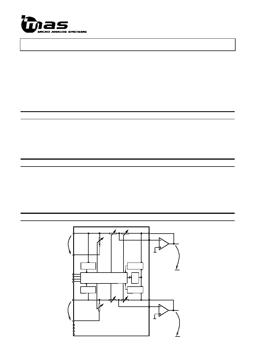
%/2&. ',$*5$0
&21752/
5
5
5
5
5
5
=(52
&5266,1*
/)2
5)2
$*1'
$9&&
9,1
9,1
9287
9287
=(52
&5266,1*
;&6
;087(
3($.
'(7(&725
'$&
3($.
'(7(&725
'$7$
/02
502
&&/.
'9&&
'*1'
/,1
5,1
5*1'
/*1'
0$6

2 (11)
DA9116.002
1 December, 2000
3,1 &21),*85$7,21
3,1 '(6&5,37,21
3LQ 1DPH
3LQ
7\SH
)XQFWLRQ
AVCC
1
P
Power Supply, for Analog
LMO
2
AI
External Amplifier Negative Input (Left)
LFO
3*
AI
Feedback Signal from External Amplifier Output (Left)
LIN
4*
AI
Input, Left Channel
LGND
5
AI
Signal Ground, Left Channel
XCS
6
DI
Chip Select Input of Serial Interface
DVCC
7
P
Power Supply, for Digital
XMUTE
8
DI
Mute Input
DATA
9
DIO
Data Input and Output of Serial Interface, Tristate
CCLK
10
DI
Clock Input of Serial Interface
DGND
11
G
Ground for Digital
RGND
12
AI
Signal Ground, Right Channel
RIN
13*
AI
Input, Right Channel
RFO
14*
AI
Feedback Signal from External Amplifier Output (Right)
RMO
15
AI
External Amplifier Negative Input (Right)
AGND
16
G
Ground for Analog
*) Note: Pins 3, 4, 13 and 14 are only 300V HBM ESD protected
502
5)2
5,1
;&6
&&/.
'$7$
'*1'
$9&&
/02
/)2
/,1
$*1'
;087(
'9&&
/*1'
5*1'
62

3 (11)
DA9116.002
1 December, 2000
*(1(5$/ '(6&5,37,21
0DLQ IHDWXUHV
MAS9116 is a stereo digital volume control designed
for audio systems. The levels of the left and right
analog channels are set by the serial interface. Both
channels can be programmed independently.
Resistor values are decoded to 0.5 dB resolution by
using internal multiplexers for a gain from ≠111.5 to
+15.5 dB. The code for ≠112 dB activates mute for
maximum attenuation. MAS9116 operates from
single +5V supply and accepts input levels up to
±18V.
,QWHUIDFHV
Control information is written into or read back from
the internal register via the serial control port. Serial
control port consists of a bi-directional pin for data
(DATA), chip select pin (XCS) and control clock
(CCLK) and supports the serial communication
protocol. All control instructions require two bytes of
data.
To shift the data in CCLK must be pulsed 16 times
when XCS is low. The data is shifted into the serial
input register on the rising edges of CCLK pulses.
The first 8 bits contain address information. The
second byte contains the control word. XCS must
return to high after the second byte. The instruction
actually takes effect on the 17th rising edge of
CCLK. That is, after the 16th CCLK XCS must be
returned to high. Then the instruction is executed on
the next CCLK. See the timing diagram on page 8.
The same process takes place for reading the
information. XCS will remain low for next 16 CCLK
pulses. The data is shifted out on the falling edges
of CCLK. When XCS is high, the DATA pin is in high
impedance state, which enables DATA pins of other
devices to be multiplexed together.
On the PCB board the same DATA and CCLK lines
can be directed to every MAS9116 chip. If the XCS-
pin is not active (low), DATA-pin of that chip is in
high-impedance state. This allows using a simple
PCB board for multichannel audio systems.
2SHUDWLQJ PRGHV
When power is first applied, power-on reset
initializes control registers and sets MAS9116 into
mute state. The activation of the device requires that
XMUTE pin is high and a control byte with a greater
than the default value is written in the gain register. It
is possible to return to the mute stage either by
setting XMUTE pin low or writing zero (00hex) to the
gain register. For device testing XMUTE pin is
bidirectional. When the test register bit 1 is high
XMUTE pin is output pin. Internal signals can be
directed to the pin.
&KDQJLQJ WKH JDLQ RI WKH FKDQQHO
When new gain value is written into the gain register
the chip will activate zero crossing and delay
generator enable signal for the selected channel.
MAS9116 will wait until falling edge zero crossing in
input signal. To ensure that there is no audible click
from the output of amplifier configuration when gain
is changed. LIN is the input line for left channel and
RIN for right channel. If there are no zero crossings
in the signal the gain is changed anyway after 18ms.
Delay generator will provide about 100ns pulse after
18ms when it is enabled.
Programming both gain registers at same time sets
gain values first to the right channel and then to the
left channel.
3HDN /HYHO 'HWHFWLRQ
MAS9116 has an 8-bit digital-to-analog converter
(DAC) used for monitoring the peak level of the
signal. The reference value is programmed via the
serial interface. The reference value VREF is
calculated from VREF=k/256x18V, where k is the
binary value of the control byte and 18V is a typical
signal value. When positive peak signal level
exceeds this value, comparator signal sets bits 0
and 1 of the status register. The register contents
stay high until the peak register has been read.

4 (11)
DA9116.002
1 December, 2000
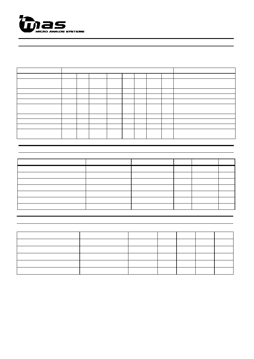
5(*,67(5 '(6&5,37,21
5HJLVWHU
$GGUHVV %\WH
'DWD %\WH
7
6
5
4
3
2
1
0
msb...lsb
Function
Peak Detector Status
CR4
X
1
0
1
1
R/W
X
X
Output code
00000000
00000001
00000010
00000011
No overload
Right overload
Left overload
Both overload
Peak Detector Reference
CR3
X
1
1
0
0
R/W
X
X
Input code
11111111
11111110
11111101
∑
∑
00000010
00000001
00000000
DAC output
255/256 AVCC
254/256 AVCC
253/256 AVCC
∑
∑
2/256 AVCC
1/256 AVCC
AGND
Left Channel Gain
CR2
X
1
1
0
1
R/W
X
X
Input code
11111111
11111110
11111101
∑
∑
11100000
00000010
00000001
00000000
Gain dB
+15.5
+15.0
+14.5
∑
∑
0.0
-111.0
-111.5
mute
Right Channel Gain
CR1
X
1
1
1
0
R/W
X
X
Input code
11111111
11111110
11111101
∑
∑
11100000
00000010
00000001
00000000
Gain dB
+15.5
+15.0
+14.5
∑
∑
0.0
-111.0
-111.5
mute
Test, CR5
X
1
1
1
1
R/W
X
X
Reserved
Both Channel Gains
X
1
0
0
1
W
X
X
Write to both gain registers
Address byte bits:
∑
Bit 2 is read/write bit (1=read, 0=write).
∑
X is don't care, recommended high for low
power.
Data byte bits:
∑
All registers get their default value 00Hex except
CR3 which gets FFHex during power-on reset.
∑
Default value for all bits is zero (00hex).
5 (11)
DA9116.002
1 December, 2000
7(67 5(*,67(5 &5 '(6&5,37,21
XMUTE pin is output pin when bit 1 is set in register CR5. Bits 2, 3 and 4 select different internal signals. In test
phase those signals can be seen via XMUTE pin.
&RQGLWLRQ
'DWD %\WH ELWV
)XQFWLRQ
7
6
5
4
3
2
1
0
XMUTE=in
0
0
0
0
0
0
0
1
Force to latch the new gain
value to resistor network
Test, XMUTE=out
0
0
0
0
0
0
1
0
left delay generator
Test, XMUTE=out
0
0
0
0
0
1
1
0
left peak detector
Test, XMUTE=out
0
0
0
0
1
0
1
0
left zero crossing
Test, XMUTE=out
0
0
0
0
1
1
1
0
left enable for zeroc and delay
generator
Test, XMUTE=out
0
0
0
1
0
0
1
0
right delay generator
Test, XMUTE=out
0
0
0
1
0
1
1
0
right peak detector
Test, XMUTE=out
0
0
0
1
1
0
1
0
right zero crossing
Test, XMUTE=out
0
0
0
1
1
1
1
0
right enable for zeroc and
delay generator
$%62/87( 0$;,080 5$7,1*6
3DUDPHWHU
6\PERO
&RQGLWLRQV
0LQ
0D[
8QLW
Signal Voltage
RIN, RFO, LIN, LFO
-20
+20
V
Positive Supply Voltage
AVCC, DVCC
-0.5
+6.0
V
All other pins
-0.5
AVCC +0.5
Storage Temperature
TS
-55
+125
o
C
Operating Temperature
TA
-40
+85
o
C
ESD (HBM) pins 3, 4, 13 and 14
300
V
ESD (HBM) all other pins
2000
V
5(&200(1'(' 23(5$7,21 &21',7,216
3DUDPHWHU
6\PERO
&RQGLWLRQV
0LQ
7\S
0D[
8QLW
Signal Voltage
RIN, RFO, LIN, LFO
-18
+18
V
Positive Supply Voltage
AVCC,DVCC
4.5
5
5.5
V
Negative Supply Voltage
AGND,DGND
0
V
Signal Grounds
LGND,RGND
0
V
Operating Temperature
TA
-20
+25
+60
o
C